

Page 1
Product Service Manual – G225HQ
Service Manual for acer: G225HQ
P/N: 9J.11016.L1A
9J.11016.41A
Applicable for All Regions
Version: 001
Date:2009/9/7
Notice:
- For RO to input specific “Legal Requirement” in specific NS regarding to responsibility and liability
statements.
First Edition (Sept, 2009)
© Copyright Acer Corporation 2009. All Right Reserved.
- 1 -
Page 2

Content Index
1. About This Manual .............................................................................................................. 3
1.1. Trademark ........................................................................................................................ 3
2. Introduction ......................................................................................................................... 4
2.1. RoHS (2002/95/EC) Requirements .................................................................................. 4
2.2. Safety Notice .................................................................................................................... 4
2.3 .Compliance Statement ..................................................................................................... 4
2.4. General Descriptions ....................................................................................................... 4
3. Product Overview ................................................................................................................ 5
3.1. Introduction ...................................................................................................................... 5
3.2. Operational Specification ................................................................................................. 7
3.3. Operational & Functional Specification .......................................................................... 12
3.4. LCD Characteristics ....................................................................................................... 16
3.7. Pallet & Shipment .......................................................................................................... 19
3.8. Certification .................................................................................................................... 20
3.9 Packing ........................................................................................................................... 22
4. Disassembly /Assembly .................................................................................................... 23
4.1. Exploded View ............................................................................................................... 23
4.2. Disassembly /Assembly ................................................................................................. 25
5. Level 1 Cosmetic / Appearance / Alignment Service ......................................................... 35
5.1 Alignment procedure (for function adjustment) ................................................................ 35
5.2 Software / Firmware Upgrade Process ........................................................................... 38
5.3 EDID Upgrade Procedure ............................................................................................... 43
5.4 OSD Operation Guide ..................................................................................................... 46
6. Level 2 Circuit Board and Standard Parts Replacement ................................................... 50
6.1. Trouble Shooting Guide ................................................................................................. 50
6.2 Circuit Operation Theory ................................................................................................. 56
6.3 Spare Parts List ............................................................................................................... 59
Appendix 1 – Screw List / Torque .......................................................................................... 62
Appendix 2 – Physical Dimension Front View and Side view................................................ 65
Appendix 3 – I/F Board ......................................................................................................... 67
- 2 -
Page 3

Abbreviations & Acronyms
1. About This Manual
This manual contains information about maintenance and service of acer products. Use this manual to
perform diagnostics tests, troubleshoot problems, and align the acer product.
1.1. Trademark
The following terms are trademarks of Acer Inc. :
Acer
Importance
Only trained service personnel who are familiar with this Acer Product shall perform service or
maintenance to it. Before performing any maintenance or service, the engineer MUST read the “Safety
Note”.
- 3 -
Page 4

2. Introduction
This section contains general service information, please read through carefully. It should be stored for
easy access place for quick reference.
2.1. RoHS (2002/95/EC) Requirements
– Applied to all countries require RoHS.
The RoHS (Restriction of Hazardous Substance in Electrical and Electronic Equipment Directive) is a legal
requirement by EU (European Union) for the global electronics industry which sold in EU and some counties
also require this requirement. Any electrical and electronics products launched in the market after June 2006
should meet this RoHS requirements. Products launched in the market before June 2006 are not required to
compliant with RoHS parts. If the original parts are not RoHS complaints, the replacement parts can be non
ROHS complaints, but if the original parts are RoHS compliant, the replacement parts MUST be RoHS
complaints.
If the product service or maintenance require replacing any parts, please confirming the RoHS requirement
before replace them.
2.2. Safety Notice
1. Make sure your working environment is dry and clean, and meets all government safety requirements.
2. Ensure that other persons are safe while you are servicing the product.
DO NOT perform any action that may cause a hazard to the customer or make the product unsafe.
3. Use proper safety devices to ensure your personal safety.
4. Always use approved tools and test equipment for servicing.
5. Never assume the product’s power is disconnected from the mains power supply. Check that it is
disconnected before opening the product’s cabinet.
6. Modules containing electrical components are sensitive to electrostatic discharge (ESD). Follow ESD safety
procedures while handling these parts.
7. Some products contain more than one battery. Do not disassemble any battery, or expose it to high
temperatures such as throwing into fire, or it may explode.
8. Refer to government requirements for battery recycling or disposal.
2.3 .Compliance Statement
Caution: This Optical Storage Product contains a Laser device. Refer to the product specifications and your
local Laser Safety Compliance Requirements.
2.4. General Descriptions
This Service Manual contains general information. There are 3 levels of service:
Level 1: Cosmetic / Appearance / Alignment Service
Level 2: Circuit Board or Standard Parts Replacement
Level 3: Component Repair to Circuit Boards
- 4 -
Page 5

3. Product Overview
Feature items
Specifications
Remark
Panel supplier & module name
LGD LM215WF1-TLA1
AUO M215HW01
TN, Normally white
Screen diagonal
21.5”W
495.5(H) x 292.2(V)
Display Format
1920(H) x 1080 (V)
Panel Display information
Pixel Pitch
LGD: 0.248 mm x 0.248 mm
SEC: 248.25 um x 248.25
um
per one triad
Viewing Angle (@ Contrast Ratio >= 10)
R/L:170 degrees (typ)
U/D: 160 degrees (typ)
Analog interface with Scaling supported
Yes
With 15-pin D-sub
connector
HDMI interface with Scaling supported
No
Max resolution mode supported
1920 (H) x 1080(V)@60Hz
Number of Display Colors supported
16.7 Millions
Contrast Ratio
LGD:
1000:1 (typ.), 700:1(min)
AUO:
1000:1 (typ.), 600:1(min)
Test Condition: Set Contrast
at 50, Brightness at 100,
Color at User preset
Luminance
300 cd/m2 (typ.),250 cd/m2
(min)
Test Condition: Set Contrast
at 50, Brightness at 100,
Color at User preset
AC power input
Yes
90-264 Volts, 47-63 Hz.
DC power input (with AC power adapter)
No DPMS supported
Yes
<2W
LED indicator for power status showed
Yes
White/Amber
OSD for control & information supported
Yes
3.1. Introduction
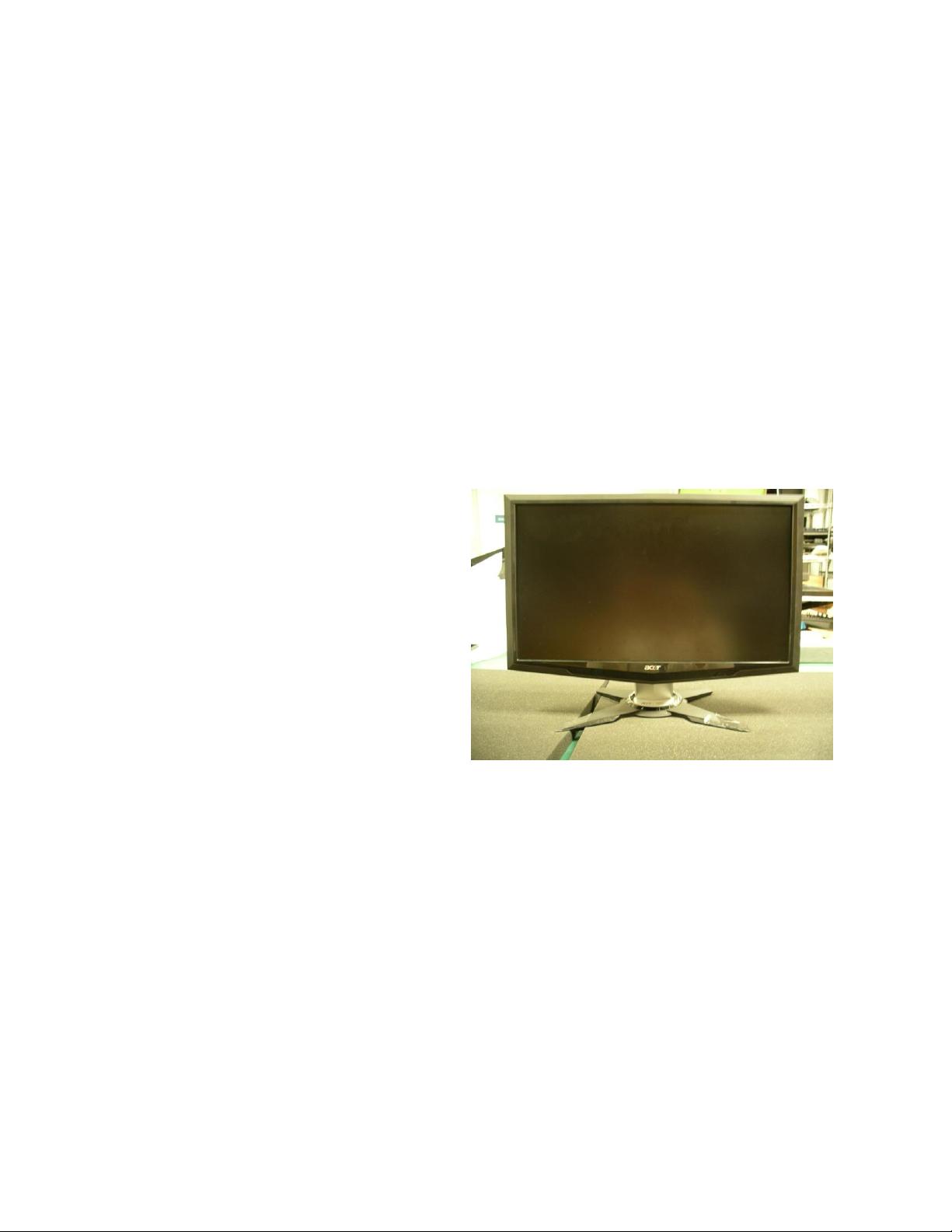
G225HQ is defined as our new 21.5”W model in ACER V series which will be the ACER project in Qisda.
G225HQ is defined as 21.5”W LCD Monitor supports 1920(H) x 1080(V) resolution with DPMS (Display Power
Management System) and ACER eColor function. There are double input types, D-sub and DVI. G225HQ
adopts LGD panel LM215WF1-TLA1, AUO panel M215HW01 . G225HQ has included 1W+1W speaker.
G225HQ also support ACM 50000:1.
The features summary is shown as below,
*All panel spec. in Q201 definition depends on the variance of panel source.
*All spec. of monitor need to warm up at least 1hr.
* To test the “Contrast Ratio” and “Luminance” functions, the color status must be “User preset” mode.
* 1. “Contrast Ratio”: Set “brightness” at 100, and “contrast” at 50.
* 2. “Luminance”: Set “brightness” at 100, and “contrast” at 100.
- 5 -
Page 6
Multi-language supported for OSD
Yes
EMEA
Non-EMEA
Buttons control supported
Yes
6 buttons including 1
monitor power on/off
control button.
Flywheel control supported
No Scaling function supported
Yes
Auto adjustment function supported
Yes
“Auto-Key” function
DDC function supported (EDID ver. 1.3)
Yes
DDC2B
DDC-CI support version 1.1 or later
Yes
DDC-CI
Audio speakers supported
Yes
Audio Jack (input connector) supported
Yes
Line-in connector
Earphone Jack (Output connector)
supported
No
Microphone function supported
No Mechanical Tilt base design
Yes
From -5 to +23 degree
VESA wall mounting design
Yes
Mechanical Rotate design
No Mechanical Lift base design
No Kensington compatible lock design
Yes
- 6 -
Page 7
Item
Condition
Spec
OK
N.A
Remark
Input Voltage range
Universal input full range
90~264VAC /47~63Hz
Input Current range
90 ~ 264VAC
< 2.0 Arms
Power Consumption
Normal “On” operation
< 52 W
LED: Blue
DPMS
DPMS “Sleep” state
< 2 W
LED: Amber
DPMS
DPMS “Off” state
< 1 W
LED: OFF
Inrush Current
110 VAC
220 VAC
< 30 A (peak)
< 60 A (peak)
Cold-start
Earth Leakage Current
264 VAC/50Hz
< 3.5 mA
Hi-Pot
1. 1500VAC, 1 sec
2. Ground test: 30A,
1sec
Without damage
< 0.1 ohm
(on-line test)
(in-lab test)
Power Line Transient
IEC1000-4-4
1KV
IEC1000-4-5 (Surge)
Common: 2KV,
Differential: 1KV
CCFL operation range
90 ~ 264VAC
LGD: 3~8mA
SEC : 4~8mA
Depends on panel
source
CCFL Frequency
90 ~ 264VAC
40KHz ~ 60KHz
Depends on panel
source
Power cord
Color: Black
Length: 1800 +/- 50 mm
3.2. Operational Specification
3.2.1 Power supply
- 7 -
Page 8
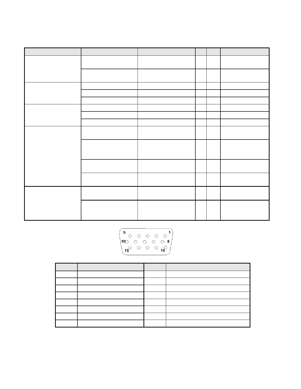
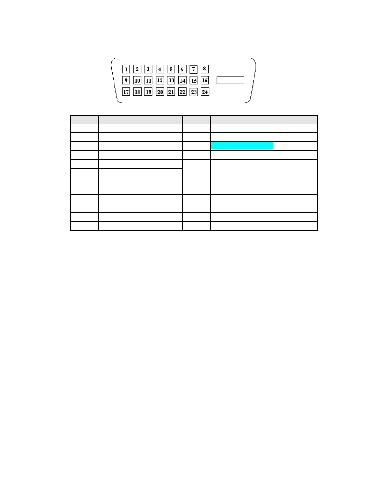
3.2.2 Signal interface
Item
Condition
Spec
OK
N.A
Remark
Signal Cable
15-pin D-Sub
Color: Black
Length: 1800 +/- 30 mm
24-pin DVI-D
Color: Black
Length: 1800 +/- 50 mm
Pin assignment
15-pin D-sub connector
See Note-1
For 15-pin D-sub
24-pin DVI-D connector
See Note-2
For 24-pin DVI-D
19-pin HDMI connector
See Note-3
For 19-pin HDMI
Analog input
Signal type
Separate analog R/G/B
For 15-pin D-sub
Level
700 mV (peak to peak)
Impedance
75 Ohms +/- 1.5 Ohms
Sync input
Signal type
Separate H/V-sync
(Positive/Negative)
For 15-pin D-sub
Level
Logic High: 2.4V ~ 5.5V
Logic Low: 0V ~ 0.5V
(TTL level)
Refer to VESA VSIS
Standard V1R1
Impedance
Minimum 2.2KΩ(pull
down)
10KΩ for application
Sync Pulse Width (SPW)
0.7μs < H-SPW
1H < V-SPW
Digital input
Level
600mV for each
differential line
Impedance
50 Ohm TDR Scan
needed for DVI cable and
interface board
Pin
Signal Assignment
Pin
Signal Assignment
1
Red video
9
PC5V (+5 volt power)
2
Green video
10
Sync Ground
3
Blue video
11
Ground
4
Ground
12
SDA
5
Cable Detected
13
H-Sync (or H+V)
6
Red Ground
14
V-sync
7
Green Ground
15
SCL
8
Blue Ground
Note-1: The pin assignment of 15-pin D-sub connector is as below,
- 8 -
Page 9
Note-2: The pin assignment of 24-pin DVI-D connector is as below,
Pin
Signal Assignment
Pin
Signal Assignment
1
TMDS RX2-
13
Floating
2
TMDS RX2+
14
+5V Power
3
TMDS Ground
15
Ground(Cable Detect)
4
Floating
16
Hot Plug Detect
5
Floating
17
TMDS RX0-
6
DDC Clock
18
TMDS RX0+
7
DDC Data
19
TMDS Ground
8
Floating
20
Floating
9
TMDS RX1-
21
Floating
10
TMDS RX1+
22
TMDS Ground
11
TMDS Ground
23
TMDS Clock+
12
Floating
24
TMDS Clock-
- 9 -
Page 10
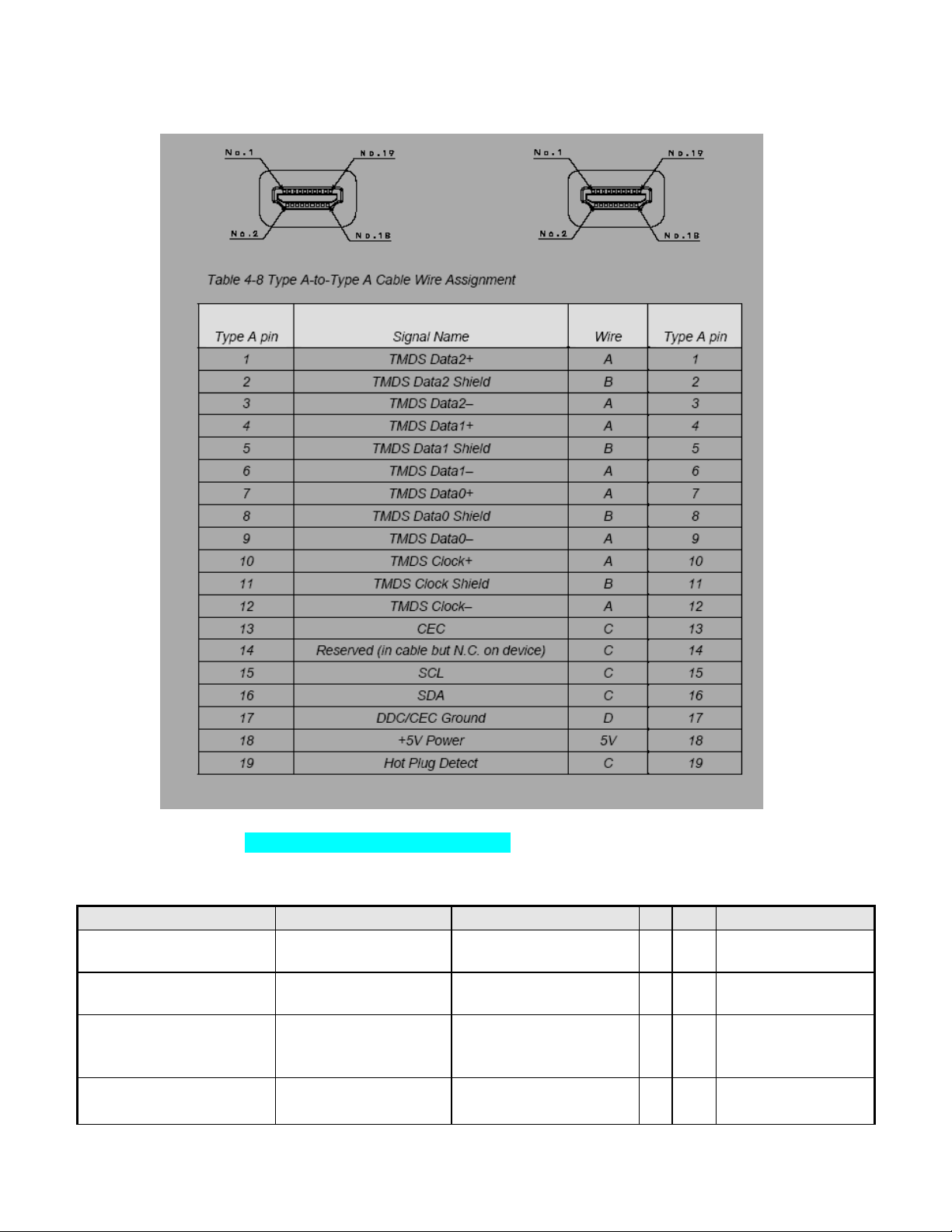
Note-3: The pin assignment of 19-pin HDMI connector is as below,
Item
Condition
Spec
OK
N.A
Remark
Max. support Pixel rate
173 MHz
Both for analog and
digital inputs
Max. Resolution
1920 x 1080
Both for analog and
digital inputs
Rise time + Fall time
< 5 ms
(50% of minimum pixel
clock period)
1920x1080 @ 60Hz
(max. support timing)
Settling Time after
overshoot /undershoot
< 5% final full-scale value
Refer to VESA VSIS
Standard V1R1
Note:Pin 11 is used as Cable Detect.
3.2.3 Video performance
- 10 -
Page 11
Overshoot/Undershoot
< 12% of step function
voltage level over the full
voltage range
Refer to VESA VSIS
Standard V1R1
Item
Condition
Spec
OK
N.A
Remark
Horizontal
31-83 KHz
Vertical
56-76 Hz
HDMI supports 50Hz
Item
Condition
Spec
OK
N.A
Remark
DDC channel type
DDC2B
EDID
Version 1.3
Refer to S/W spec.
document to see the
detailed EDID data
definition.
DDC-CI
Version 1.1 or Later
Refer to S/W spec
3.2.4 Scan range
3.2.5 Plug & Play DDC2B DDC-CI Support
- 11 -
Page 12

3.2.6 Support Timings
Mode
Resolution
(active dot)
Resolution
(total dot)
Horizontal
Frequency (KHz)
Vertical
Frequency (Hz)
Nominal Pixel
Clock (MHz)
640x480@60Hz
800 x 525
31.469
59.941
25.175
640x480@72Hz
832 x 520
37.861
72.809
31.500
MAC
640x480@66.66Hz
864x525
35
66.66
30.24
VESA
720x400@70Hz
900x449
31.469
70.087
28.322
SVGA
800x600@56Hz
1024 x 625
35.156
56.250
36.000
800x600@60Hz
1056 x 628
37.879
60.317
40.000
800x600@72Hz
1040 x 666
48.077
72.188
50.000
1024x600@60Hz
1312x622
37.320
60.000
48.964
XGA
1024x768@60Hz
1344x806
48.363
60.004
65.000
1024x768@70Hz
1328x806
56.476
70.069
75.000
VESA
1152x864@75Hz
1600x900
67.5
75
108
1280x960@60Hz
1800x1000
60
60
108
SXGA
1280x1024@60Hz
1688x1066
63.981
60.020
108.000
VESA
1280x720@60Hz
1650x750
44.955
59.940
74.176
WXGA
1280x800@60Hz
1680x831
49.702
59.810
83.500
1360x768@60Hz
1792x795
47.712
60.015
85.500
WXGA+
1440x900@60Hz
1904x931
55.935
59.887
106.500
WSXGA+
1680x1050@60Hz
2240*1089
65.290
59.954
146.250
UXGA
1600x1200@60Hz
2160x1250
75.000
60.000
162.000
1920x1080@60Hz
2576x1120
67.158
59.963
173.000
1920x1080@60Hz
2200x1125
67.500
60.000
148.500
1920x1080@60Hz
2080x1111
66.587
59.934
138.500
Note:
3.3. Operational & Functional Specification
3.3.1 Video performance
- 12 -
1. Show “Input Not Supported” warning message.
When Vertical Frequency is over 76Hz or under 56Hz, the display is Black and showing “Input Not
Supported” warning message. (Some video timings are except for PAL, 50Hz signals.)
2. If Hf /Vf is set in the range of 31KHz~83KHz and 56Hz ~76Hz (not including some video timing), and
Pixel Clock is set in the range of 25.175MHz~173MHz(DVI and HDMI input port 165MHz for SingleLink), but is not the above Resolution, then it will display the nearest mode.
3. When digital input 1680x1050@75Hz and 1920x1080@60Hz_CVT, because of TMDS Pixel Clock is
setting in the range of 25MHz~165MHz, the source may use Dual-Link signal to transmit the timing.
This model can only support Single-Link to receive the information of half-of- Dual-Link, the display
may be abnormal.
Page 13

*All spec. of monitor need to warm up at least 1hr.
Item
Condition
Spec
OK
N.A Remark
Resolution
Any input resolution modes
which are under
1920x1080
1920x1080
Contrast ratio
700(min),1000(typ.)
Test Condition: Set
Contrast at 50,
Brightness at 100,
Color at User preset.
Brightness
At R/G/B saturated
condition
300 cd/m2 (typ.),250 cd/m2
(min)
Test Condition: Set
Contrast at 50,
Brightness at 100,
Color at User preset.
Response time
Rising + Falling time
On/off:5 ms
(typ.),10ms(max)
Test Equipment:
Westar TRD 100 or
equal level
equipment ;
Viewing angle
At Contrast ratio = 10
R/L: 170 degrees (typ.)
140 degrees (min)
At Contrast ratio = 10
U/D:160 degrees (typ.)
130 degrees(min)
CIE coordinate of White
(0.313, 0.329) +/- (0.03,
0.03)
Display colors
16.7 Millions colors
6 bit+Hi-FRC
Item
Condition
Spec
OK
N.A Remark
Resolution
Any input resolution modes
which are under
1920x1080
1920x1080
Contrast ratio
600(min),1000(typ.)
Test Condition: Set
Contrast at 50,
Brightness at 100,
Color at User preset.
Brightness
At R/G/B saturated
condition
300 cd/m2 (typ.),240 cd/m2
(min)
Test Condition: Set
Contrast at 50,
Brightness at 100,
Color at User preset.
Response time
Rising + Falling time
On/off:5 ms (typ.),8ms(max)
Test Equipment:
Westar TRD 100 or
equal level
equipment ;
Viewing angle
At Contrast ratio = 10
R/L: 170 degrees (typ.)
150 degrees (min)
At Contrast ratio = 10
U/D:160 degrees (typ.)
140 degrees(min)
CIE coordinate of White
(0.313, 0.329) +/- (0.03,
0.03)
Display colors
16.7 Millions colors
6 bit+Hi-FRC
LGD LM215WF1-TLA1/TLB1
AUO M215HW01 V0/V1
- 13 -
Page 14

3.3.2 Brightness Adjustable Range
Item
Condition
Spec
OK
N.A Remark
Brightness adjustable
range
At default contrast level
(saturate point) & Fullwhite color pattern
(Max. brightness value –
Min.
brightness
value)
≧ 100 cd/㎡
Item
Condition
Spec
OK
N.A Remark
Acoustical Noise
At 30 cm distance
≦ 22 dB/A
Refer to C326
Item
Condition
Spec
OK
N.A Remark
Temperature
Operating
0 ~ +40 ℃
Non-operating
-20 ~ +60 ℃
Humidity
Operating
10 ~ 90%
Non-condensing
Non-operating
10 ~ 90%
Non-condensing
Altitude
Operating
0~3048m (10,000ft)
Without packing
Non-operating
0~12,192m (40,000ft)
With packing
Item
Condition
Spec
OK
N.A Remark
(1) Vibration
Package, Non-Operating
Test Specification:
1. Frequency Hertz 5 ~
250 HZ , PSD Level
0.0054 (G2/Hz)
2. Grms = 1.146
3. Sweep Time : 30
minutes per Axis
4. Axes : X,Y,Z
(2) Unpackaged Vibration
Unpackaged, Non-
Operating
Test Spectrum:
20 Hz 0.0185(g2/Hz)
200Hz 0.0185(g2/Hz)
Duration : 5 Minutes
Axis : 3 axis ( Horizontal
and Vertical axis ,Z axis)
(3) Drop
Package, Non-Operating
76 cm Height (MP stage)
(1 corner, 3 edges, 6 faces)
(4) Shock
Wooden package, Non-
Operating
1. Amplitude : Half sine-wave
50G
2. Duration : 10 ms
3. Test Times : 1
4.Test Sides : All 6 Sides
3.3.3 Acoustical Noise
3.3.4 Environment
3.3.5 Transportation
- 14 -
Page 15

Item
Condition
Spec
OK
N.A Remark
Electrostatic Discharge
IEC801-2 standard
Contact: 8KV
Air: 15KV
Item
Condition
Spec
OK
N.A Remark
TCO03
Electric
Band 1 < 10 V/m
Band 2 < 1 V/m
Magnetic
Band 1 < 200nT
Band 2 < 25nT
EMI
FCC part 15J class B
After Mass production
under 1dBuv for constant
measure. Besides DNSF
and VCCI class-2 are
optional.
EN55022 class B
Item
Condition
Spec
OK
N.A Remark
MTBF Prediction
Refer to MIL-217F
> 60,000 Hours
Excluding
CCFL
CCFL Life time
At 25±2℃, under 7.0mA
40,000 Hours (min)
See Note-4
Item
Condition
Spec
OK
N.A
Remark
Preamp + Power amp
(1)Output power
1 Wrms/CH @ 1KHz
(2)THD (@ 1W)
<1%
(3)S/N ratio >40dB
Speaker Driver
(1)Nominal impedance
8 ohm
(2)Rated input power
1 W/CH
(3)Frequency response
180~20KHz SPL-10dB
(4)Output sound pressure
level
84 ± 3 dB (1W 0.5M)
(5)Dimension of box
284x60x27mm2
Audio Control
(1)Volume range
0 ~100 levels
(2)Mute On/Off
3.3.6 Electrostatic Discharge Requirements
3.3.7 EMC
3.3.8 Reliability
Note-4: CCFL lifetime is determined as the time at which brightness of lamp is 50%. The typical lifetime of
CCFL is on the condition at 7.0mA lamp current.
3.3.9 Audio performance
- 15 -
Page 16
Item
Condition
Spec
OK
N.A Remark
LCD Panel Supplier
LGD
Panel type of Supplier
LGD LM215WF1 TLA1
Screen Diagonal
546.86mm(21.53”)
Display area
Unit=mm
476.64(H) x 268.11(V)
Physical Size
Unit=mm
495.6(H) x 292.2(V) x 16.5(D)
Weight
Unit=gram
2100 (typ.)
Technology TN type
Pixel pitch
Unit=um
248(H) x248 (W)
Per one triad
Pixel arrangement
R/G/B vertical stripe
Display mode
Normally White
Support color
16.7Millions colors
6 bit + HiFRC
Item
Condition
Spec
OK
N.A Remark
LCD Panel Supplier
AUO
Panel type of Supplier
AUO M215HW01
Screen Diagonal
546.86mm(21.5.”)
Display area
Unit=mm
476.64(H) x 268.11(V)
Physical Size
Unit=mm
495.6(H) x 292.2(V) x 16.35(D)
Weight
Unit=gram
2188 (typ.)
Technology TN type
Pixel pitch
Unit=um
248.25(H) x248.25 (W)
Per one triad
Pixel arrangement
R/G/B vertical stripe
Display mode
Normally White
Support color
16.7Millions colors
6 bit + HiFRC
Item
Unit
Conditions
Min.
Typ.
Max.
Remark
Viewing Angle
[degree]
[degree]
Horizontal (Right)
CR = 10 (Left)
140
170
-
-
[degree]
[degree]
Vertical
(Up)
CR = 10 (Down)
130
160
-
-
Contrast ratio
Normal Direction
700
1000
Response Time
[msec]
Rising Time
-
1.3
2.6
3.4. LCD Characteristics
3.4.1-1 The Physical definition & Technology summary of LCD panel
LGD LM215WF1 TLA1
AUO M215HW01
3.4.2-1 Optical characteristics of LCD panel
LGD LM215WF1 TLA1
- 16 -
Page 17
[msec]
Falling Time
-
3.7
7.4
[msec]
Rising + Falling
- 5 10
Color / Chromaticity
Coordinates (CIE)
Red x 0.646
Red y 0.334
Green x
0.303
Green y
0.616
Blue x 0.147
Blue y 0.067
Color Coordinates (CIE)
White
White x
0.313
White y
0.329
Luminance Uniformity
[%]
9 points
measurement
75
White Luminance @ CCFL
7.0mA (center)
[cd/m2]
250
300
-
Crosstalk (in 75Hz)
[%]
1.5
* The test methods for the above items’ definition, please refer to the relative panel specification.
Item
Unit
Conditions
Min.
Typ.
Max.
Remark
Viewing Angle
[degree]
[degree]
Horizontal (Right)
CR = 10 (Left)
150
170
-
-
[degree]
[degree]
Vertical
(Up)
CR = 10 (Down)
140
160
-
-
Contrast ratio
Normal Direction
600
1000
[msec]
Rising + Falling
- 5 8
Color / Chromaticity
Coordinates (CIE)
Red x
0.618
0.648
0.678
Red y
0.309
0.339
0.369
Green x
0.252
0.282
0.312
Green y
0.573
0.603
0.633
Blue x
0.113
0.143
0.173
Blue y
0.040
0.070
0.100
Color Coordinates (CIE)
White
White x
0.283
0.313
0.343
White y
0.299
0.329
0.359
Luminance Uniformity
[%]
9 points
measurement
75
80
White Luminance @ CCFL
7.0mA (center)
[cd/m2]
240
300
-
Item
Condition
Spec
OK
N.A
Remark
Power button
Auto button(Exit button)
Right/Inc. button
Left/Dec. button
AUO M215HW01
3.5.1 User’s hardware control definition
- 17 -
Page 18
Menu button
Mode button
Input Select button
E-Key button
Mute button
Item
Condition
Spec
OK
N.A
Remark
Auto Adjust
Auto-Geometry
Brightness
Contrast
Horizontal Position
Vertical Position
Pixel Clock
Phase
Color
Cool(9300K)
Warm(6500K)
User: Separate R/G/B
adjustment
OSD Position
OSD Horizontal position
OSD Vertical position
OSD Time
From 10 sec to 120 sec
OSD Lock
Language
EMEA/Non-EMEA
languages for Asia/Europe
Version
Recall
Recall All
Mode
ACER Empower Mode
Input Select
D-sub
DVI
HDMI
Wide Mode
Full
Aspect
Sharpness
Display Information
For input timing
Volume
Mute
Hot key for Auto
Hot key for Contrast
Hot key for Volume
Hot key for Input Select
Hot key for Mode
3.5.2 OSD control function definition
- 18 -
Page 19
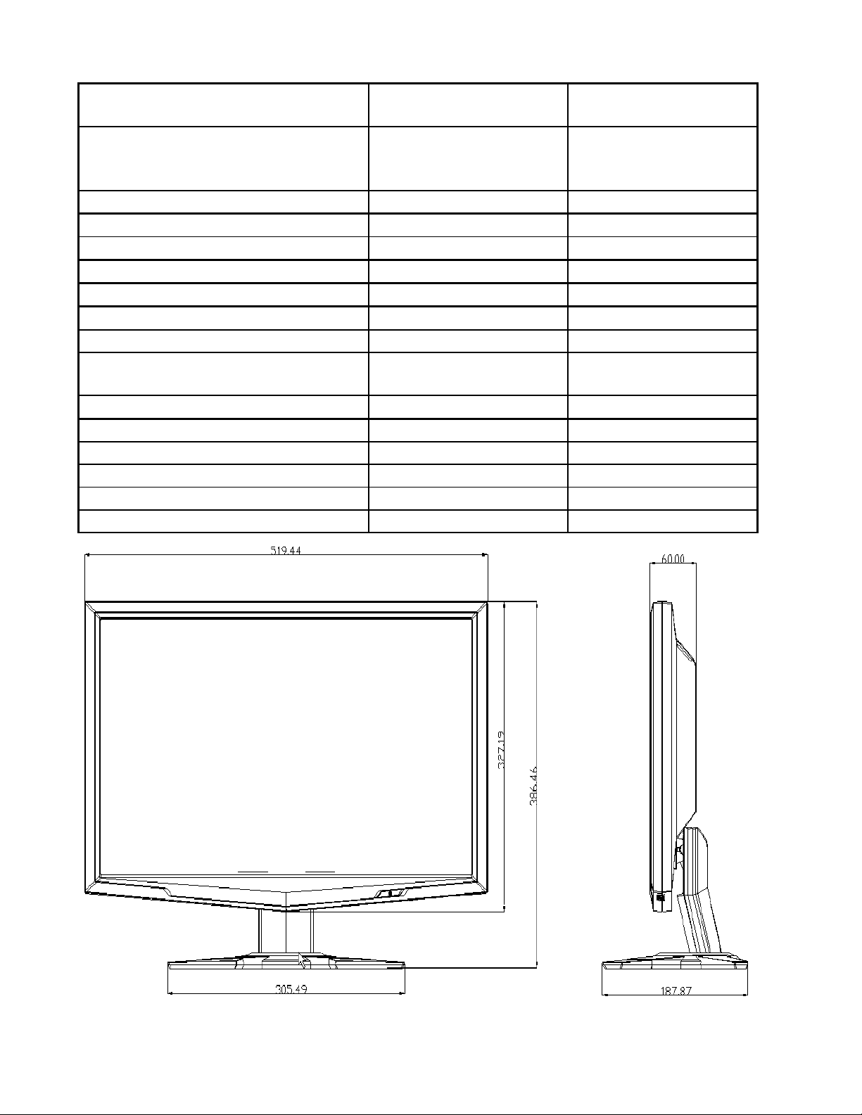
3.6.1 Dimension
Item
Condition
Spec
OK
N.A
Remark
Bezel opening
478.24*269.71 mm
Monitor without Stand
W x H x D mm
519.44*327.19*60mm
Monitor with Stand
W x H x D mm
519.44*386.46*187.87mm
Carton Box (outside)
L x W x H mm
142*568*452mm
Tilt and Swivel range
Tilt: -3.5 ~ +15 degree
Swivel: 0 degree
Item
Condition
Spec
OK
N.A
Remark
Monitor (Net)
4.288 kg
Monitor with packing
(Gross)
6.006 Kg
Item
Condition
Spec
OK
N.A
Remark
Flammability
>ABS<,94-HB
Heat deflection To
ABS
65 ℃
UV stability
ABS
Delta E < 8.0
Resin
ABS
Texture
Uc+CLUM-R+BASE:ATIM-D02;
Bezel : AT-IM-D01+Polish
#10000
CLUM-F+BTN OSD : ATIM-D01
BTN PWR: Polish #10000
Color
BEZEL : DT02A;
UC: DB27A
Item
Condition
Spec
OK
N.A
Remark
Color
Kraft
Material
B Flute
Compression strength
200KGF
Burst Strength
16 KGF/cm2
Stacked quantity
4 Layers Vertical
Stowing Type
Quantity of products
(sets)
(Every container)
Quantity of Products
(sets)
(Every Pallet)
Quantity of pallet
(sets)
(Every Container)
With pallet
20'
720
Pallet A: 72
Pallet A: 10
Pallet B: --
Pallet B:
3.6.2 Weight
3.6.3 Plastic
3.6.4 Carton
3.7. Pallet & Shipment
3.7.1 Container Specification
- 19 -
Page 20
40'
1440
Pallet A: 72
Pallet A: 20
Pallet B: --
Pallet B:
Without pallet
20'
X X X
X X X
40'
X X X
X X X
Net Weight (Kg)
Gross Weight (Kg)
Dimension w/o Base
W*H*D (mm)
Dimension w/ Base
W*H*D (mm)
4.288 Kg
6.006 Kg
519.44*382.53*60
519.44*386.46*187.87
Carton Interior Dimension (mm)
L*W*H
Carton External Dimension (mm)
L*W*H
134 x 560 x 440
142x568x452
Item
Condition
Spec
OK
N.A
Remark
Environment
Green design
API Doc. 715-C49
ISO14000
Requirement
Blue Angel
German Standard
E-2000
Switzerland
EPA
USA Standard
TCO’99
TCO’03
MPR2
Green Mark
PC-Monitor
Microsoft Windows
PC98/99
DPMS
VESA
DDC 2B
Version 1.3
USB
External
Safety
UL (USA)
UL60950 3rd edition
CSA (Canada)
CAN/CSA-C22.2 No.
60950
Nordic / D.N.S.F
EN60950
FIMKO
EN60950
CE Mark
73/23/EEC
CB
IEC60950
CB
EN60950
3.7.2 Carton Specification
3.7.2.1 Product:
3.7.2.2 Package:
3.8. Certification
- 20 -
Page 21
TUV/GS
EN60950 /
EK1-ITB 2000:2003
CCC (China)
CB4943
GOST
EN60950
TUV type-approved
SASO
IEC60950
EMC
CE Mark
89/336/EEC
FCC (USA)
FCC Part 15 B
EN55022
Class B
CISPR 22
Class B
VCCI (Japan)
VCCI Class B
BSMI (Taiwan)
CNS 13438
C-Tick (Australia)
AS/ NZS CISPR22
X- Ray Requirement
DHHS (21 CFR)
USA X- Ray Standard
DNHW
PTB
German X- Ray
standard
Ergonomics
TUV / Ergo
ISO 13406-2
prEN50279
- 21 -
Page 22
3.9 Packing
- 22 -
Page 23

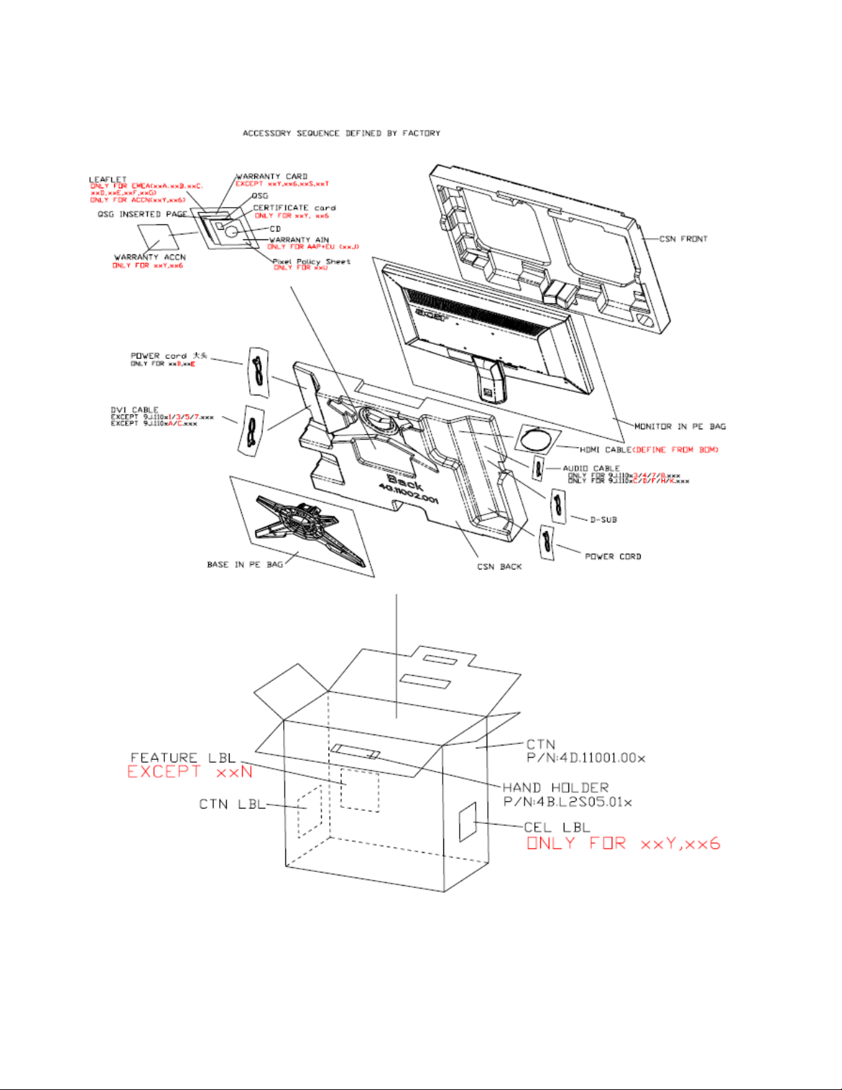
4. Disassembly /Assembly
4.1. Exploded View
- 23 -
Page 24

- 24 -
Page 25

ite
m
picture
Operation
Tool
Notes
1
Stick the big Al tape to
panel which can protect
the Light-wire.
The tape must cover
the connect of the
wire
2
Check and put CLM-F on
the cushion carefully,
3
Assemble the panel on
CLM-F.
4
Assembly the Ctrl board
to CLM-F.
4.2. Disassembly /Assembly
Assembly SOP about G225HQ
Preparation before assemble
1.Clean the room for work
2.Identify the area for material
3.Prepare the implement, equipments, materials as bellow:
1) Press-fixture
2) working table
3) Screw-driver
4) knife*1
5) Glove
6) Cleaning cloth
7) ESD protection
- 25 -
Page 26

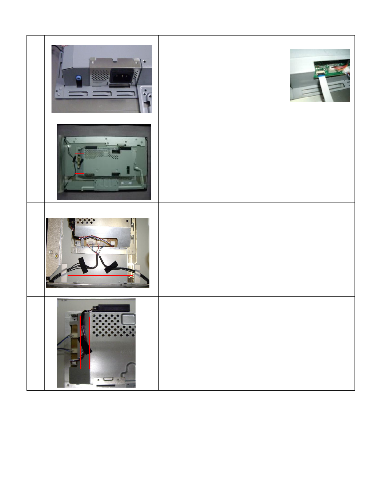
5
Tear down the two tape
behind the FFC and fix
the FFC of C/B to panel
The FFC must be
affixed besides the
under edge of the
panel
6
Assemble the SPK to the
main-SHD, the correct
position reference on the
picture, then the lock 4
screws to fasten it.
Screw-driver
7
Assemble the LVDS to the
I/F, the correct position
reference on the picture
Without the gap within
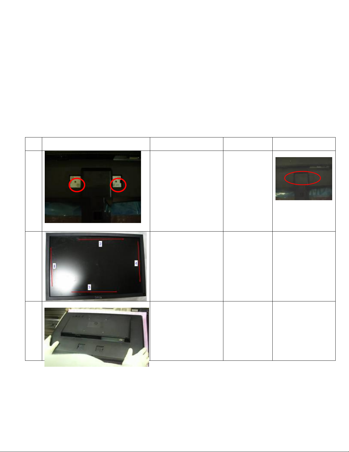
NOTE: Circuit boards >10 cm² has been highlighted with the yellow rectangle as
above image shows. Please detach the Circuit boards and follow local regulations for
disposal.
8
Assemble the PCBA to
Main-SHD
- 26 -
Page 27

9
Lock 5 screws on the
PCBA board with this
order.
Screw-driver
11
Lock one grounded
screws on the SPS board
with order.
Screw-driver
Make sure the wire
doesn’t walk across
the red area
12 Scan for fooling
PC
Card go with panel.
13
Fasten the LVDS to panel
and fix the Main-BKT to
CLM-F
The BKT must fixed
into the clip of the BZL
14
Stick three Al foils on the
right and under between
panel and Main-BTK
Only for the monitor
with LGD panel which
has two lamps
接地螺丝
2
1
4
3
5
- 27 -
Page 28
15
Assemble the L-SHD the
correct position reference
on the picture. Insert the
FFC cable of control
board into the connector
of I/F board
16
Insect the inverter wire
one by one .
Keep all wires in.
17
Stick two acetic tapes to
fix the wire one by one as
the picture .
The wires must not
over the edge of the
Panel
18
Insect the speaker wire
to the right position
of the power board.
Then stick a acetic
tape to fixing the wire
as the picture.
Make sure the wire
between the mark on
the main-SHD and the
surface of the mainSHD.
- 28 -
Page 29
19
Stick a acetic tape to
fixing the speaker wire
as the picture.
20
Lock screws of side on
Main-Chassis with
2/4,based on DVI.
Screw-driver
Attention the order by
one to four.
21
Fix the big Al tape to
panel
22 Assemble the Rear Cover.
3
4
1
2
- 29 -
Page 30

23
Lock the screw of the rear
cover. Connect the DSUB wire to the D-SUB
connect.
Screw-driver
24
Check and put CLM-F-abs
on working table the
carefully. Lock 4 screws
inside the hinge.
Screw-driver
25
Lock 4 screws to RC. And
then cover the CLM of L
and R.
Screw-driver
- 30 -
Page 31
Disassembly SOP about G225HQ
ite
m
picture
Operation
Tool
Notes
1
Disassemble the stand
4 screws. Take off the
stand then unlock the
screw of rear cover.
Screw-driver
Kick the board first.
2
disassembly the bezel
from the monitor, notice
the disassembly order :
1.Left (1) parts of bezel
2.Top (2) parts of bezel
3.Bottom (3) parts of
bezel
4. Right (4) parts of bezel
Don’t draw the BZL
When disassembly
the bezel ,notice don’t
bend the C/B .man
must wear glove
The purpose is loose
the BZL
3
Turn over the
monitor ,dismantle the
Rear cover from the
monitor.
Preparation before disassemble
1.Clean the room for disassemble
2.Identify the area for monitor
3.Check the position that the monitors be placed and the quantity of the monitor ;prepare the area for material
flow; according to the actual condition plan the disassemble layout
4.Prepare the implement, equipments, materials as bellow:
1) Press-fixture
2) Working table
3) Screw-driver
4) Knife*1
5) Glove
6) Cleaning cloth
7) ESD protection
- 31 -
Page 32

4 Tear down the Mylar
5 Tear out the acetic tapes
6
Unlock the wires.
7
Disassembled the SHD
shielding : 2/4 screw(the
monitor with DVI have
four)
Screw-driver
3 4 1
2
- 32 -
Page 33

8
Tear down three pieces of
Al foils
9
Disassembled the AC-soc
shielding .
10 Unlock the FFC wire.
11
Disassembled the PCBA
shielding : 6 screws
Screw-driver
NOTE: Circuit boards >10 cm² has been highlighted with the yellow rectangle as
above image shows. Please detach the Circuit boards and follow local regulations for
disposal.
- 33 -
Page 34

12
Disassembled the SPK
shielding : 4 screws
Screw-driver
13
Get off the panel from the
bezel
14
Get off the big tap
from the tape
15
Disassemble the control
board
Screw-driver
- 34 -
Page 35

Mode
Resolution
(active dot)
Resolution
(total dot)
Horizontal
Frequency (KHz)
Vertical
Frequency (Hz)
Nominal Pixel
Clock (MHz)
640x480@60Hz
800 x 525
31.469
59.941
25.175
640x480@72Hz
832 x 520
37.861
72.809
31.500
MAC
640x480@66.66Hz
864x525
35
66.66
30.24
VESA
720x400@70Hz
900x449
31.469
70.087
28.322
SVGA
800x600@56Hz
1024 x 625
35.156
56.250
36.000
800x600@60Hz
1056 x 628
37.879
60.317
40.000
800x600@72Hz
1040 x 666
48.077
72.188
50.000
1024x600@60Hz
1312x622
37.320
60.000
48.964
XGA
1024x768@60Hz
1344x806
48.363
60.004
65.000
1024x768@70Hz
1328x806
56.476
70.069
75.000
5. Level 1 Cosmetic / Appearance / Alignment Service
5.1 Alignment procedure (for function adjustment)
5.1.1 Preparation:
1.) Setup input timing to any preset modes or patterns.
2.) Enter factory mode (press “Empowering” & “Power” buttons at the same time to turn on monitor).
3.) Move cursor into “Burn-in Mode” tag and select “On” to enable burn-in mode.
4.) Power off the monitor, remove the input source and then power on again.
5.) Setup unit and keep it warm up for at least 30 minutes.
6.) Setup input timing ICL-605( 1280x1024@75Hz ), 32-Grays pattern.
7.) Setup unit and keep it warm up at least 30 minutes.
5.1.2 Timing adjustment: (Analog only, it is not required for DVI-D input source)
1.) Enter factory setting area (press “Empowering” and then press “SOFTPOWER”).
2.) Check the settings to following values:
Contrast = 50
Brightness = 77
Color = Warm
Language = English
Then, turn off the monitor power.
3.) Turn on power enter user area.
Figure-1: Preset Timing modes list
- 35 -
Page 36

VESA
1152x864@75Hz
1600x900
67.5
75
108
1280x960@60Hz
1800x1000
60
60
108
SXGA
1280x1024@60Hz
1688x1066
63.981
60.020
108.000
VESA
1280x720@60Hz
1650x750
44.955
59.940
74.176
WXGA
1280x800@60Hz
1680x831
49.702
59.810
83.500
1360x768@60Hz
1792x795
47.712
60.015
85.500
WXGA+
1440x900@60Hz
1904x931
55.935
59.887
106.500
WSXGA+
1680x1050@60Hz
2240*1089
65.290
59.954
146.250
UXGA
1600x1200@60Hz
2160x1250
75.000
60.000
162.000
1920x1080@60Hz
2576x1120
67.158
59.963
173.000
1920x1080@60Hz
2200x1125
67.500
60.000
148.500
1920x1080@60Hz
2080x1111
66.587
59.934
138.500
Color temperature
X+-
0.283+(-) 0.03
Y+-
0.297+(-) 0.03
5.1.3 ADC calibration (Auto color balance adjustment)
~~Analog only, it is not required for DVI-D input source
1. Setup input timing ICL-605( 1280x1024@75Hz ), pattern 42(5-Mosaic pattern with white color block)
with Analog signals from Chroma video pattern generator. (it depends on Scaler IC supplier’s
recommendation)
2. Enter factory mode (press “Empowering” & “Power” buttons at the same time to turn on monitor).
3. Move cursor into “Burn-in Mode” tag and select “On” to enable burn-in mode.
4. Close OSD menu then press “Auto” button for auto color adjustment. (This procedure will get optimal
gain/offset(clamp) values)
5. Checking if the picture is ok, or reject this monitor and check its circuit board or wire/cable connection.
5.1.4 Color temperature adjustment
1. Setup input timing to any preset modes, pattern 41(full white color pattern) with Analog signals from
Chroma video pattern generator.
2. Enter factory mode (press “Empowering” & “Power” buttons at the same time to turn on monitor).
- 36 -
3. Move cursor into “Burn-in Mode” tag and select “On” to enable burn-in mode.
4. Make sure ADC calibration (auto color balance adjustment) had already been done.
5. Measure color temperature by Minolta CA-110 (or equivalent equipment).
6. Adjust the color temperature ~~ Two methods can be used to adjust RED, GREEN, BLUE value of
each color temperature, C0/Cool, C1/User & C2/Warm to meet following spec requirement, the 1st
method is by using external PC and IIC alignment protocol to do automatic adjustment, and the 2nd
method is by manually and must be in factory mode.
Page 37

(C0/cool on OSD)
Luminance
Color temperature
(C1/User on OSD)
X+- Y+- Luminance
Color temperature
(C3/Warm on OSD)
X+-
0.313+(-) 0.03
Y+-
0.329+(-) 0.03
Luminance
7. Move cursor into “Burn-in Mode” tag and select “No” to disable burn-in mode.
8. Turns off the monitor power.
5.1.5. Writing EDID data into monitor
1. Setup a PC with DDC card.
2. Connect PC to monitor with a D-sub signal cable.
3. Please refer to the Q212 for the correct EDID file.
4. Runs the writing program to write the analog EDID data into EEPROM for analog input(ie. 15-pin D-
sub).
5. Repeat step 4 and write the digital EDID data into EEPROM for DVI-D input(ie. 24-pin DVI-D).
6. Read both EEPROM data and confirm it to match with the Q212 definition.
(Note : The DVI-D input may not operation correctly if the digital EDID data do not exist.)
- 37 -
Page 38

Connect to target monitor
VGA signal input from 15pin D-sub
cable of PC or NB.
Connect ISP board and PC
with printer port cable
Check the Jumpers on the
ISP Circuit Board (make sure
J5, J6, J7, J8 are set at ping
1,2 )
5.2 Software / Firmware Upgrade Process
5.2.1 Hardware prepared:
Hardware Requirement:
1. ISP board x 1
2. DSUB VGA cables x 2
3. Printer cable (with one male connector and another female connector) x 1.
4. PC or Notebook with parallel (printer) port x1.
- 38 -
Page 39

5.2.2 Firmware Upgrade Procedure
Step 1:
Un-zip Port95nt and install into your computer.
Step 2:
Un-zip ISP application tool (RTDTool)
Step 3:
Select IIC and RTD 2122 type, then press “ISP” button to execute firmware program application.
- 39 -
Page 40

Step 4:
Select File type to Bin and ISP address to 0X90
Press “Bigbin” button to load *series*.bin file from your computer.
Step 5:
Select “Erase” option and execute lightning button first, and then select “Auto” option and execute
lightning button to start upgrade firmware to the monitor.
Note: you can change program speed bar to meet your equipment speed if program firmware fail in
Advanced Setting.
- 40 -
Page 41

5.2.3 Turn Off Burn In
ENTER and RIGHT to Burn In Off
IF the monitor without signal input has Burn In pattern. As the following figure
Press “"E-key" +" Power"” key at the same time to exit Burn in mode(factory mode),and soft power key
off/on restart the monitor.
- 41 -
Page 42

5.2.4 Setup the OSD for Panels
Timing request: 1280X1024@75Hz
1. Press the OSD setting
2. Choose “On” in Burn In
Choose “Panel Type” to press Enter.
4. Choose the Panel Type you want (LGD
or SEC), and press Enter.
3. Change Color temperature to “user”
mode
- 42 -
5. Check OSD to make sure the panel type
is match with your panel.
Page 43

5.3 EDID Upgrade Procedure
Step 1:
Run the program “Q-EDID-V012.exe”, when the UI popped up
Note: If “VGA” choose 128bytes, and “HDMI” choose 256bytes
- 43 -
Page 44
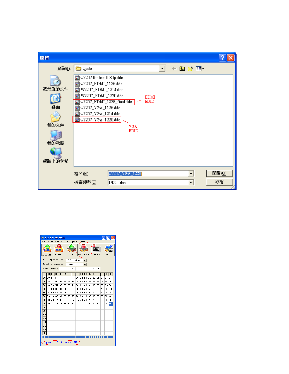
Step 2:
Click “Open File” and select “VGA” or “HDMI” EDID file
Step 3:
If load file is successful, it shows “Open EDID Table OK..”.
And then, Click “Write EDID” button to update EDID
v
- 44 -
Page 45

Step 4:
If write EDID is successful, it shows”Write EDID OK …”
And then, Click “Read EDID” button to check if successful or not.
Step 5:
If read EDID is successful, it shows”Read EDID OK …”
- 45 -
Page 46

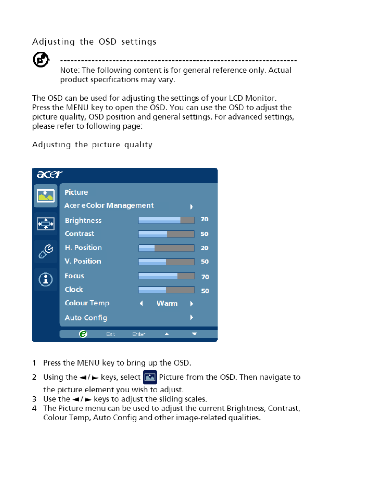
5.4 OSD Operation Guide
- 46 -
Page 47

- 47 -
Page 48
- 48 -
Page 49

- 49 -
Page 50

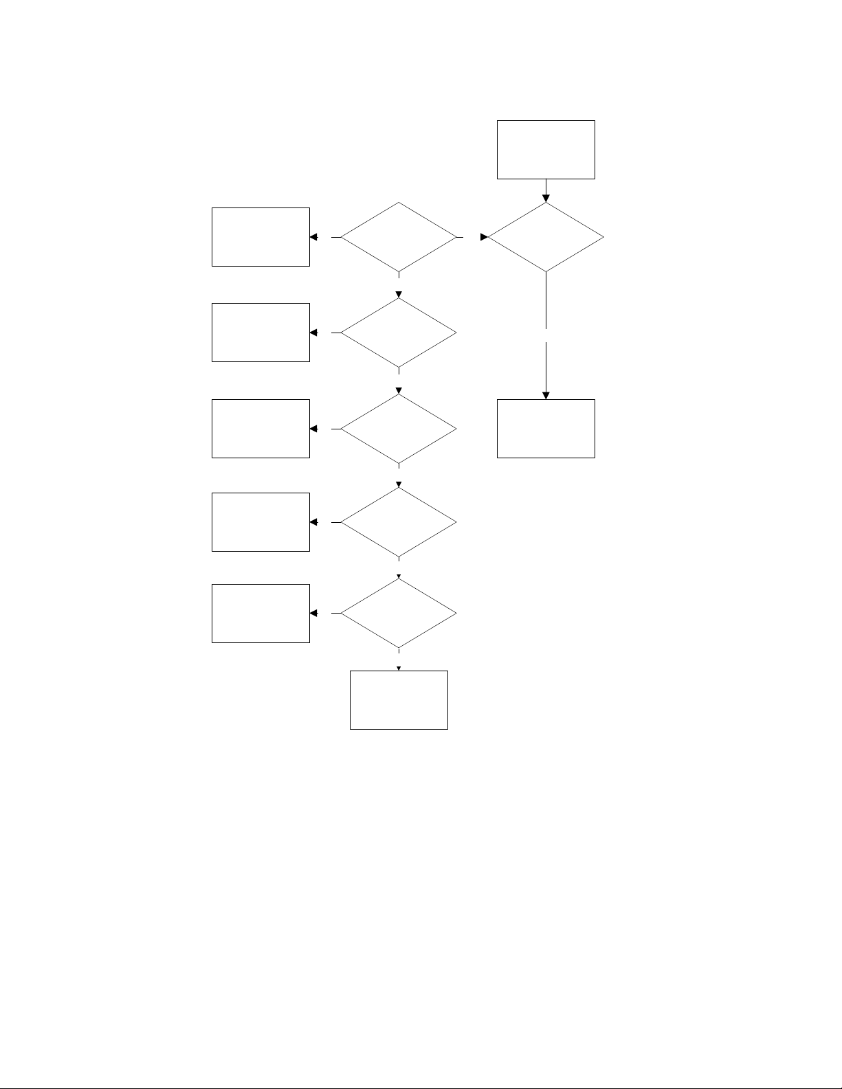
OSD shown when key pressed?
No
Yes
Follow instructions from OSD dialog
Keypad OK?
Yes
No
Screen is Blank and
Power LED is White.
Backlight turned
ON?
Scalar output
Data ?
Yes
Proceed to
“Check Power Board”.
No
Yes
“Check LCD Module”
No
Proceed to
“Check Scalar”
Proceed to
“Check Control Board”.
6. Level 2 Circuit Board and Standard Parts Replacement
6.1. Trouble Shooting Guide
1. No Display or display is unstable (Interface Board):
- 50 -
Page 51

Checking Contorl
Board
Working ?
Yes
Yes
No
Re-plug the control
wire, then retry
Traces
OK ?
No
Replace the Control
Board, then retry
Components to
Control board OK ?
Yes
No
Replace the
components, then retry
Replace a new Control
board
Yes
2. Check Control Board
- 51 -
Page 52

3 Check Scalar
Are all the power and
ground pins at the correct
voltage level?
Are the correct RGB and
Hsync signal fed to
Scalar ?
Scalar failed
to output data
YES
YES
NO
NO
Capacitors of Crystal
have damaged
Check the remaining
circuits
Measure the signal pairs
on LVDS data output and
clock from Scalar
Is the correct Sinusoidal
wave appeared on Crystal
YES
Are the pixel output
correct?
Are the signals presented
on DSub connector?
Scalar failed
Power or the ground pins
has bad contacts
DSUB Connector or
PC failure
Bad wiring between
DSUB and Scalar
NO
NO
YES
YES
NO
- 52 -
Page 53

LCD module fail
To display
image
White ScreenNo Picture
NO
NO
YES
Bad Connection
or connector,
LVDS cable
NO
LCM failed
Bad Connection
or connector,
LVDS cable
Bad Connection
or connector,
YES
YES
YES
NO
OK
?
YES
NO
LCD module fail
To display
image
Connection between
LVDS cable and
LCM connector
OK ?
White ScreenNo Picture
Lamp connector OK ?
NO
NO
YES
Connection between
LVDS cable and
LVDS connector
OK?
Bad Connection
or connector,
LVDS cable
NO
Bad Connection
or connector,
LVDS cable
Bad Connection
or connector,
YES
YES
YES
NO
Lamp wire
Inverter board
failed
YES
NO
Is Q6 5V? Check Q6
Check U7
Is U7 5V?
4 Check LCD Module
- 53 -
Page 54

5 Power Board no work troubleshooting:
No Backlight
V-inverter ok? No
Check
D703/D704
OK?
No
Yes
Replace D703/D704No
Check F601,
Q601, R615 OK?
Yes
Replace F601,
Q601, R615.
No
Check I/F BD
Yes
+5V ok?
Yes
Check CN701 pin2
(BL-ON) is Hi?
Yes
Check CN701 pin1
(BRT-ADJ) exist?
Yes
Check I/F BD
Yes
Replace IC801 No
Yes
Replace Q808,
Q810, T801, T802.
No
Check Panel
Yes
No
No
Check
D701/D702
OK?
Replace D701/D702
No
Check Q808, Q810,
T801, T802 OK?
Check IC801
OK?
- 54 -
Page 55
6 Audio Function:
Was Audio Input
plugged?
Yes
Return Power
Function Step.
No Yes
Was Audio VDD
existed?
Audio do not work
No
Check VOL_ON
Yes
Check VOL_ADJ
Plug Audio input.
No
Check MCU send
VOL_ON control
signal or not.
No
Adjust volume
control switch to
normal.
Yes
Was CN551
plugged?
NoPlug CN551
Yes
Was Speaker
plugged?
NoPlug Speaker.
Yes
Replace IC551.
- 55 -
Page 56

6.2 Circuit Operation Theory
I. Introduction:
G225HQ is a 21.5 inch and 24bits color TFT LCD monitor, which can support the resolution up to 1920x1080. It
has VGA input and compliant with VESA specification to offer a smart power management. The monitor has
DDC/CI function to make the monitor communicate with PC by Acer ADM DDC/CI software, and also it has
ACM function to let the monitor contrast ratio up to 50000:1. It also offers OSD Menu for users to control the
adjustable items and get some information about this monitor.
II. Block diagram
G225HQ consists of a main body and a stand (base). The main body contains a AUO/LGD TFT
LCD module with 4 CCFL lamps, a power board (includes AC/DC、 DC/DC、 inverter and
panel power source), a control board and an interface board. The block diagram is shown as
below.
Fig. Block diagram for G225HQ LCD monitor
- 56 -
Page 57

III. Circuit Implementations:
A.) THE MAIN BODY:
A-1.) Interface board block diagram:
(a) Circuit operations:
The scaling IC has OSD and auto detecting input timing functions. OSD offers adjustable functions to the endusers. Auto detecting timing function can detect change modes. It outputs the digital R-G-B data, pixel clock
and control signal to TCON of the LCD module. A MCU, build in scaling IC (Realtek2545LH), is responsible for
the system processing. There are two external storing units, one is 24C16 to store the OSD function data and
user preset timings.
(b) IC introduction:
1.) Realtek2555LH SCALER IC:
Realtek2555LH series products are all-in-one LCD monitor controller with analog (RGB), DVI and video inputs,
supporting 1920x1080@60Hz ,and integrate Realtek high performance ADC,scaling engine,LVDS Tx,and so
on.Moreover,all products are pin compatible in QFN 48-pin package to save cost and make the design easier.
The RTD also includes an ITU656 video format input port with color space converter that makes it an attractive
solution for low cost MFM and TV applications. The output section contains a 24-bit TTL output interface and a
channel LVDS transmitter for direct interfacing of commercially available LVDS LCD panel modules. In addition,
- 57 -
Page 58

RTD2555LH embedded 16.5KSRAM dynamically stores OSD command and fonts, compatible advanced color
EMI Filter
Rectifier and
filter
Isolation
power
transformer
Rectifier and
filter
Inverter circuit
PWM contrller
Switching
element
+5V Output
Feedback
Isolation
Rectifier and
filter
LDO regulator
L602
20MH
1
2
4
3
C602
0.22U M
C603
1000P M
C604
1000P M
C601
0.22U M
N1
N3
L6
control features.
2.) EEPROM:
We use 24C16 EEPROM to store monitor user data and user preset timings. There are 16 user timing modes
are automatically saved in it. Each timing mode is allocated with 22 bytes of memory space for information such
as Sync frequencies, polarities… etc. PC can access the EEPROM data indirectly through the SDA and SCL
channels of DVI and D-sub (IIC communication). The digital and analog DDC data are stored in two 24C02s
EEPROM.
A-2.) Power board diagram:
Fig.1
#1 EMI Filter
This circuit (Fig.2) is designed to inhibit electrical and magnetic interference for meeting FCC, VDE, VCCI
standard requirements.
- 58 -
Page 59

Picture
CATEGORY
DESCRIPTION
ACER PART NO.
LCD
LCDM21.5W
LM215WF1-TLB1
LGD P
LK.21508.002
Board
BOARD
PCBA IF BD DUAL
A/L MI G225HQ
55.LJA0Q.001
BOARD
PCBA SPS BD
AUDIO MI G225HQ
55.LJA0Q.005
BOARD
PCBA CTRL BD MI
G225HQ
55.LJ80Q.006
Cable
6.3 Spare Parts List
- 59 -
Page 60

CABLE
CORD H05VV-F
10A250V EUR 1.8M
27.LBJ0Q.001
CABLE
WIRE 10/11-P
1007#24 X223HQ
50.LGQ0Q.004
CABLE
FFC LVDS 30P 16TH
NO S G225HQ
50.LJ80Q.002
CABLE
FFC WIRE 7P CTRL
BD G205H
50.LJ80Q.001
CABLE
CABLE SIGNAL/C
H+V OD_5.5 1.8M
50.LBJ0Q.002
Assembly
- 60 -
Page 61

CASE/COVER/BRA
CKET ASSEMBLY
ASSY BASE W/P
G225H
60.LJ80Q.008
CASE/COVER/BRA
CKET ASSEMBLY
ASSY RC DUAL LPL
G225HQ
60.LJ80Q.005
CASE/COVER/BRA
CKET ASSEMBLY
ASSY CLMN ABS
DB27A G225H
60.LJ80Q.007
CASE/COVER/BRA
CKET ASSEMBLY
ASSY BZL DB27A
G225HQ
60.LJ80Q.001
- 61 -
Page 62
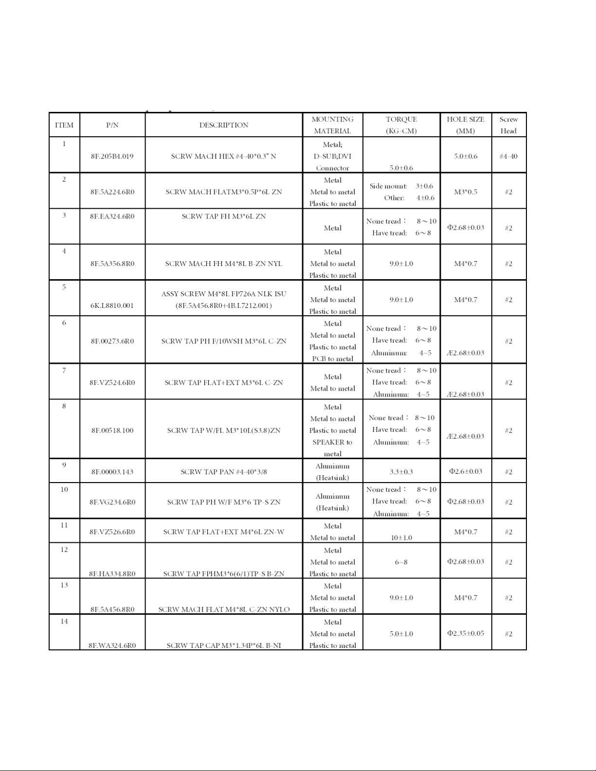
Appendix 1 – Screw List / Torque
(A)
STANDARD SCREW TORQUE QCS
- 62 -
Page 63

- 63 -
Page 64

(B)
STANDARD SCREW TORQUE QZB & QMX
- 64 -
Page 65

Appendix 2 – Physical Dimension Front View and Side view
Fig. 1 Physical Dimension Front View and Side view
- 65 -
Page 66

- 66 -
Page 67

Appendix 3 – I/F Board
Please see the next page
- 67 -
Page 68

5
4
+5V
3
2
U9 spec.
Vds =-30V , V gs=+/ -12V
Id= -3.5A wh en am bie nt te mp. =70 degre
1
D D
C C
B B
Reset circuit for CMO L03 over
rush current
C102
0.1U K
PANE L_ON
G697L293 T1UF
5
/RESET
CD
4
NC
U9
VCC
GND
R59
R307
1K J
1
2
3
R308
20K
12
+
10K J
C6 8
22U 25V
B
R60
10K J
R58
100K J
Q6
2N3904S
E C
+5V
G
C69
0. 1U K
D
S
U7
AO3401L
12
+
C6 6
22U 25V
LC D_5V_P OWER
C67
R30
150 J
0. 1U K
R31
150 J
LC D_5V_P OWER
G(1)
S(2)
R61 0 J
R62 0 J
R63 0 J
RXEI N3+
RXEI N3RXEC KIN+
RXEC LK-
RXEI N2+
RXEI N2-
RXEI N1+
RXEI N1-
RXEI N0+
RXEI N0-
RXOIN 3+
RXOIN 3-
RXOCK IN+
RXOCK IN-
RXOIN 2+
RXOIN 2-
RXOIN 1+
RXOIN 1-
RXOIN 0+
RXOIN 0-
TP5
TP6
TP9
TP10
TP11
TP12
TP13
TP14
TP15
TP16
TP17
TP18
TP19
TP20
TP21
TP22
TP23
TP24
TP1
TP2
TP3
TP4
D(3)
G1
1
2
3
4
5
6
7
8
9
10
11
12
13
14
15
16
17
18
19
20
21
22
23
24
25
26
27
28
29
30
G2
J7
G1
1
2
3
4
5
6
7
8
9
10
11
12
13
14
15
16
17
18
19
20
21
22
23
24
25
26
27
28
29
30
G2
2KK20 85030
Screw Holes
1
5
4
3
2
H1
A A
HOLE-V8
5
9
8
7
6
GN D GN D GN D
5
4
3
2
H2
HOLE-V8
1
9
8
7
6
4
5
4
3
2
H3
HOLE-V8
1
9
8
7
6
Opt ica l P oints
OP1
3
OP2
OP3
Qisda Corporation
Pro j ec t Code
Title
Pan el output
S i ze D oc um en t Number Rev.
PCB P/N
<S i z e >
4H. 0K601.S01
M on d a y , F e b r u a r y 0 9 , 2 0 0 9
D at e: S h e et
Pre p a red By
Louis Yang
2
Model Name
PCB Rev.
S 0 1
Re vie w e d By A p p rove d By
O E M/ O D M Model Name
<D o c>
1 5
Blight Hsu A llen PC Lee
1
O E M
0
of
Page 69

5
4
3
2
1
ED ID _V CC
D D
C8
0. 1U Z
C C
SD A_A
SC L_A
B B
+3 .3V PC 5V
DN 4
BA V70
A1
A2
J
U1
1
2
3
4
A0
VCC
A1
WP
A2
SCL
GND
SDA
AT 24 C02N -10S U-1.8
NC 10K J
8
7
6
5
R3 05
Q9
2N 3904 S
E DI D_V CC
E C
R5
12K J
C1 6
47 P J
R6 7
10K
D1
BZ V55 C6V2
A K
R6
12K J
R1 2
150 J
R1 1
150 J
D2
PZ U6 .2B2
A K
D3
A K
D4
PZ U6. 2B2
C1 7
47 P J
PZ U6. 2B2
R6 8
10K
R6 9
B
A_ De tec t
20K J
PZ U6. 2B2
R1 00 0 J
A K
TP41
TP42
TP43
D5
A K
TP44
R1 9
10K J
R1 7
R2 0
10K J
R1 8
T65
J 1
G1G2
6
100 J
100 J
D- sub 15
1
7
2
8
3
TP58
9
4
10
5
C2 1
22 P J
C2 0
12 P J
11
12
13
14
15
TP40
TP62
TP63
TP64
A_ De tec t
TP59
TP38
TP60
TP39
TP61
A_ De tect
HS 1
R1
75 J
L1
R1 +
+3.3 V
K
DN 1
C1
J
BA V99
VS1
G 1+
BA V99
B1+
BA V99
DN 2
DN 3
0. 1U Z
A
R2
75 J
+3.3 V
K
C2
J
0. 1U Z
A
R3
75 J
+3.3 V
K
C3
J
0. 1U Z
A
Z60
L2
Z60
L3
Z60
C5
4. 7P C
C6
4. 7P C
C7
4. 7P C
R4
R9
R1 0
R1 3
R1 4
R1 5
100 J
56 J
100 J
56 J
100 J
56 J
C9 0. 04 7U 16 V
C1 1 0 .0 47U 16V
C1 2 0 .0 47U 16V
C1 3 0 .0 47U 16V
C1 4 0 .0 47U 16V
C1 5 0 .0 47U 16V
RE D1 -
RE D1 +
GR EE N1-
GR EE N1+
BL UE1 -
BL UE1 +
A A
5
4
3
2
Qisda Corporation
Pro ject Code
Title
D-S UB INPUT
Size D ocu ment Number Rev.
PCB P/N
<S i z e >
4H. 0K4 01.S01
M o n d a y , F e b r u a r y 0 9 , 2 0 0 9
D ate: Sheet
Pre p ared By
Louis Yang
Mod el Name
PCB Rev.
S 0 1
Re view e d By A p p roved By
Bli ght Hsu Allen PC Lee
1
O E M /O D M Model Name
OE M
< D o c >
of
1 6
0
Page 70

5
4
3
2
1
0824 C84 from 10U ==>100U
0824 Add C301
0824 Add R301 R302
D D
0912 L4 ==> R100
0912 MTV 512==>RTD 2120
1228 Add R300 R303 R304 C300 Q7
0131 Add D9
C C
B B
Qisda Corporation
Project Code
Title
History
A A
Size Document Number Rev.
PCB P/N
<S i z e >
Da te: Sheet
M on d a y , F e b r u a r y 0 9 , 2 009
Prepared By
Ev o nne Chan
5
4
3
2
Model Name
OE M/ODM Model Name
OEM
PCB Rev.
S03
Re view ed By A ppro ved By
<D oc>
of
1 5
Di o Chi ang A l l en PC Lee
1
0
Page 71

5
D D
C C
J2
RX2 -
1
1
9
9
17
17
2
2
10
10
18
18
3
3
11
11
19
19
4
4
12
12
20
20
5
5
13
13
21
21
6
6
14
14
22
22
7
7
15
15
23
23
8
8
16
16
24
24
G1
G1
G2
G2
2K2 20 0902 4
TP 66
TP 67
TP 68
TP 69
TP 57
TP5 4
TP 56
TP 55
PZ U6 .2 B2
DV I -I_ SCL
D8
A K
RX1 RX0 RX2 +RX2 +
RX1 +RX1 +
RX0 +RX0 +
D 6
PZ U6 .2 B2
D 7
BZ V5 5C6 V2
A K
TP 45
TP 46
TP 47
TP 48
TP 49
TP 50
TP 51
TP 52
DV I -I _SD A
TP5 3
RX C +
R2 3
R XC-
4.7K J
HD C P_ CT RL
A K
Lo ui s HD CP (0 116)
4
A_ D et ect
A_ D ete ct
R2 1
130 J
R2 2
130 J
D_ D e tec t
Ho t-Plu g
SC L _D
SD A_ D
DV I PC 5V
C3 3
0. 1 U Z
Ca b le_ Det ect _D
R3 04
D 9
BZ V5 5C 6V2
A K
R1 6
D_ D e tec t
47 J
1K J
WP _ DV I
3
PZ U6 .2B 2
PZ U6 .2B 2
2
RX0 -
RX0 +
RX1 -
RX1 +
RX2 -
RX2 +
R XC-
RX C +
+3 .3V
C2 2
D N 6
0. 1 U Z
BA V99
K
J
C2 3
K
A
D N 7
0. 1 U Z
J
BA V99
C2 4
K
A
D N 8
0. 1 U Z
J
BA V99
C2 5
K
A
D N 9
0. 1 U Z
J
BA V99
C2 6
K
A
DN 10
0. 1 U Z
J
BA V99
C2 7
K
A
DN 1 1
0. 1 U Z
J
BA V99
C2 9
K
A
DN 1 2
0. 1 U Z
J
BA V99
A
D1 0
C3 1
0. 1 U Z
A K
D1 1
C3 2
A K
0. 1 U Z
C3 0
DN 1 3
0. 1 U Z
BA V99
1
R110
10
RX0 M
R111 10
R112 10
R113 10
R114 10
R115 10
R116 10
RX 0P
RX1 M
RX 1P
RX2 M
RX 2P
RX CM
K
R117 10
J
RX CP
A
Ch un gHao ESD (0131)
D N 5
BA V70
J
R3 06
10K J
+3 .3V
A2
8
7
6
5
U 2
1
A0
VCC
2
A1
WP
3
A2
SCL
4
GND
SDA
AT 24C 02N -10 SU- 1. 8
C1 0
0. 1 U Z
Qisda Corporation
Pro j ect Code
DVI INPU T
Tit le
Size Doc umen t Number Rev.
PCB P/N
< S i z e >
M o n d a y , F e b r u a r y 0 9 , 2 0 0 9
Da te: Sh eet
Pre pared By
4
3
2
Lo u is Yang
M o del Name
4H.0 K401 .S01
O E M / O DM M odel Name
O E M
PCB Rev.
S 0 1
Rev iew e d By A p proved By
Bli ght Hsu A l len PC Lee
1
< D o c >
of
2 6
0
R7
12K J
C1 8
47 P J
A1
R 8
12K J
C1 9
47 P J
SC L _D
SD A_ D
WP _ DV IWP _ DV IWP _ DV IWP _ DV I
WP _ DV IWP _ DV IWP _ DV IWP _ DV IWP _ DV IWP _ DV IWP _ DV IWP _ DV IWP _ DV IWP _ DV IWP _ DV IWP _ DV IWP _ DV IWP _ DV IWP _ DV IWP _ DV IWP _ DV IWP _ DV IWP _ DV IWP _ DV IWP _ DV IWP _ DV IWP _ DV IWP _ DV I
DV I PC5 V
5
B B
A A
Page 72

5
4
3
2
1
+3.3V TMD S_ VDD
D D
12
+
R1 .8D VCC
C45
47 U 25V
C35
0. 1U Z
C36
0. 1U Z
+3.3V
C88
1U K
U12
1
IN
RM2101B0DA
3
OUT
GND
TAB
2
4
gi ach in 252 5L (0 719)
Opti on
LH-- >R 25 1k
C C
B B
U1 3
NC/ RM2 101 D0DA
1
VIN
GND
2
RXE CKIN+
RXO CKIN+
RXECLK-
RXO CKIN-
VOUT
R1 .8DV CC+3.3V
3
LR-- >R 25 6. 2k
C37
0. 1U Z
Z220
L5
12
+
C46
47 U 25V
RX2M
TMD S_ VDD
RX1P
RX1N
RX0P
RX0N
RXCP
RTD _V
R TD_H
DG ND
RTD _B-
RTD _B+
U8
10
11
12
1
2
3
4
5
6
7
8
9
G1
Copper GND
V1/REXT
V2/RX1P
V3/RX1N
V4/RX0P
V5/RX0N
V6/RXCP
V7/RXCN
AVS
AHS
ADC_GND
B-
B+
ohm
ohm
RX1P
RX1M
RX0P
RX0M
RXCP
RXCM
BL UE1-
BL UE1+
VS1
HS1
R25
1K J
TMD S_ VDD
C34
0. 1U Z
M512_XOUT
RX2P
RX2N
C RYSTA R_OUT
TMD S_V DD
48
47
46
45
XIN
V0/RX2N
TMDS_VDD
VCLK/RX2P
RTD _SCLK
SC L_D
44
DDCSCL/PWM0/TCON7
RTD _SD3/ SDI
SDA _D
RTD _SCLK
R TD_SD 3/S DI
43
42
41
SCL
DDCSDA/PWM1/I RQ/TCON9
RTD2545LH-LF
G-13G+14R-15R+16ADC_VDD17BJT_B18VCCK19PGND20TXE3+21TXE3-22TXE2+23TXE2-
RTD _G-
R TD_R-
RTD _G+ RX2P
BJT _B RT D_DD CSDA
R1 .8DV CC
R1 .8DV CC
RTD _R+
1K J
C38
0. 1U Z
R1 .8DV CC
R1 .8DV CC
SDA
RXE3+
R24
0 J
RXO IN0-
RXO IN0+
RXO0-
RXO0+
40
38
37
VCCK
PGND39TXO0-
TXO0+
TXO1-
TXO1+
TXO2-
TXO2+
TXOC-
TXOC+
TXO3-
TXO3+
TXE0-
TXE0+
TXE1-
TXE1+
24
RXE2+
RXE3-
RXE2-
TMD S_ VDD
R26 NC / 0 J
Opti on
LH-- >R 24 ,
R26 C38
LR-- >R 26 C38 ,
R24
36
35
34
33
32
31
30
29
28
27
26
25
RXO1-
RXO IN1-
RXO1+
RXO IN1+
RXO2-
RXO IN2-
RXO2+
RXO IN2+
RXOC-
RXO CKIN-
RXOC+
RXO CKIN+
RXO3-R XCN
RXO IN3-
RXO3+
RXO IN3+
RXE0-
RXE IN0-
RXE0+
RXE IN0+
RXE1-
RXE IN1-
RXE1+
RXE IN1+
RE D1-
RE D1+
R1 .8DV CC
R1 .8DV CC
GRE EN1-
GRE EN1+
TMD S_ VDD
A A
Opti on
LH-- >R 27 ,
R29 C39
LR-- >R 29 C39 ,
R27
5
4
3
R9 1
R29 NC 0 J
R27
0 J
RXE IN3+
RXE IN3-
C39
0. 1U Z
RXE IN2-
RXE IN2+
Qisda Corporation
Pro j ect Code
Tit le
Scalar
Size Document Number Rev.
PCB P/N
<S i z e >
4H.0K401.S 01
M o n d a y , F e b r u a r y 0 9 , 2 0 0 9
Da te: Sheet of
Pre p ared By
Lo uis Yang
2
Model Name
PCB Rev.
S 0 1
Rev iew e d By A p p rov ed By
O E M/O DM Model Name
OEM
< D o c >
3 6
Blight Hsu A l len P C Lee
1
0
Page 73

A
B
+3.3V
C
D
E
NC 1M
13
14X215X116
P7.7
P3.5/T1
P3.4/T0
P3.3/INT1
P3.2/INT0
RST
DA7/P5.7
DA6/P5.6
DA5/P5.5
48
R28
4.7K J
P7.6/CLKO2
NC
NC
4.7K J
R33
R30 2
C64
10 P J
12
11
10
9
8
7
6
5
4
3
2
1
R30 1
4.7K J
4.7K J
+3.3V
C10 1
1 U K
R55
4.7K J
W P_C0 4
+3.3V
C40
1 U K
+3 .3V
PWM1
VO L_A DJ
PWM0
BR T_A DJ
R56
4.7K J
Ca ble_ De tec t_D
SCL
SDA
SD A_A
SC L_A
SD A_D
SC L_D
HD CP_ CT RL
+3.3V
12
+
C61
10 U 25 C
R10 1
10K J
B/V Series Without Audio Function
R213 R30
1 Open
C101 change to 0 ohm(0603)
X Series don't have Audio Function
R213 R301 C101
R28 Open
Qisda Corporation
Pro j ec t C o de
Tit le
MCU 2120L
S iz e D o c um en t Number Rev.
PC B P/N
<S i z e >
4H. 0K401 .S01
M o n d a y , F e b r u a r y 0 9 , 2 0 0 9
D a te: S h eet
Pre p a red By
D
Lo ui s Yang
Mo de l Na m e
PC B Rev.
S 0 1
Re vie w ed By A p p r o ved By
Blight Hsu A llen PC Lee
E
O E M/ O D M Mo de l Na m e
OEM
< D o c >
4 6
o f
0
C65
17
NC18NC
VSS
HSDA1/TXD/P3.1
HSCL1/RXD/P3.0
DA0/P5.044DA1/P5.145DA2/P5.246DA3/P5.347DA4/P5.4
43
L ED _GR N
LE D_O RG
10 P J
R57
Y 1
24 MHZ
R2 07
R2 09
R2 03
+3.3V
R2 08
4.7K J
4.7K J
4.7K J
U1 0
23
24
25
P6.4
P6.5
26
P6.6/CLKO1
27
P6.7
28
VSYNC
29
NC
30
NC
31
NC
32
NC
33
P1.7
34
P1.6
35
P1.5
36
P1.4
P1.337P1.238P1.139P1.0/ET240VCC
R2 13
4.7K J
4.7K J
+5V
R21 5
R21 4
19
P6.0/AD020P6.1/AD121P6.2/AD222P6.3/AD3
RT D21 20L-L F
NC42NC
41
C62
0 .1U K
+3.3V
4.7K J
4.7K J
C
4 4
A DC_ KEY 3
A DC_ KEY 2
A DC_ KEY 1
PO WE R_K EY
3 3
2 2
+3.3V
C63
0 .1U
1 1
NVRAM
U4
1
A0
VCC
2
A1
WP
3
A2
SCL
4
GND
SDA
AT 24 C16 N-10SI -1.8
R53
R54
4.7K J
8
7
6
5
A
4.7K J
W P_C0 4
SCL
S DA
M512 _XOUT
RT D_S CLK
RT D_S D3 /SDI
SC L_T OUC H
SD A_T OUC H
PA NEL _ON
BL _ON
VO L_O N
B
L12
Z120
R2 00
R2 01
R2 02
4.7K J
4.7K J
4.7K J
Page 74

A
J5
1
1
2
2
3
3
4
4
5
5
6
6
7
2K6 118511 0
7
8
8
9
9
10
10
4 4
TP7 0
C47
0 .1U K
C48
0 .1U K
TP3 2
TP3 3
TP3 4
TP3 5
TP3 6
TP3 7
B
L8
Z30
Z220
L9
12
C50
C51
0 .1U K
C52
0 .1U K
C49
0 .1U K
+
C84
47 U 25 V
0 .1U K
BR T_A DJ
BL _ON
VO L_O N
VO L_A DJ
+5V
+3.3V
C
S CL_ TOU CH
S DA_ TOU CH
R22 0
4.7K J
R22 1
4.7K J
R21 6
R21 7 0 J
R21 8 0 J
D
0
+5V
J3
G2
7
6
5
4
3
2
1
G1
2KK 208700 7
E
+3.3V
ADC KEY R105~107,R219
R216~R218,R220~223
TOUCH KEY R105~107,R219
3 3
Canael GND to GND bead
LE D_O RG
L ED_ GRN
2 2
LE D_O RG
L ED _GR N
R216~R218,R220~223
+5V
R42
10K J
R44
10K J
2N 3906S
B
Q4
C E
B
2N 3906S
Q5
C E
R43
R45
EMI solution
150
150
C53
C54
0 .1U Z
0 .1U Z
Z220
L10
Z220
L11
A DC_ KEY 1
A DC_ KEY 2
A DC_ KEY 3
Del R219(0 ohm)
Add L4 (0 ohm)
L4
R105 2K J
R106 2K J
R107 2K J
C72
47 0P J
Z220
C73
47 0P J
C74
47 0P J
R22 3 0 J
B/V
X
Z D7
Z D6
A K
UD ZS 6. 2B
UD ZS 6. 2B
Z D9
UD ZS 6. 2B
TP2 6
TP2 7
TP2 8
TP2 9
TP3 0
TP3 1
Z D8
A K
A K
UD ZS 6. 2B
A K
R22 2
4.7K J
J6
PO WE R_K EY
J3
2K6 209510 7
7
6
5
4
3
2
1
J6
Qisda Corporation
1 1
A
B
C
D
Pro j ec t C o de
Tit le
Con nector
S iz e D o c um en t Number Rev.
PC B P/N
<S i z e >
4H. 0K401 .S01
M o n d a y , F e b r u a r y 0 9 , 2 0 0 9
D a te: S h eet
Pre p a red By
Lo ui s Yang
Mo de l Na m e
PC B Rev.
S 0 1
Re vie w ed By A p p r o ved By
B l i gh t Hsu A l l en PC Lee
O E M/ O D M Mo de l Na m e
OEM
< D o c >
5 6
o f
E
0
 Loading...