

Page 1
E900WA Service Manual
t
Power saving
1. Mode:1280×1024@60Hz
2. Pattern: full white
at each modes
3. Brightness: Max.
4. Contrast: Defaul
Power Key Off
5. Level 2 Circuit Board and Standard Parts Replacement
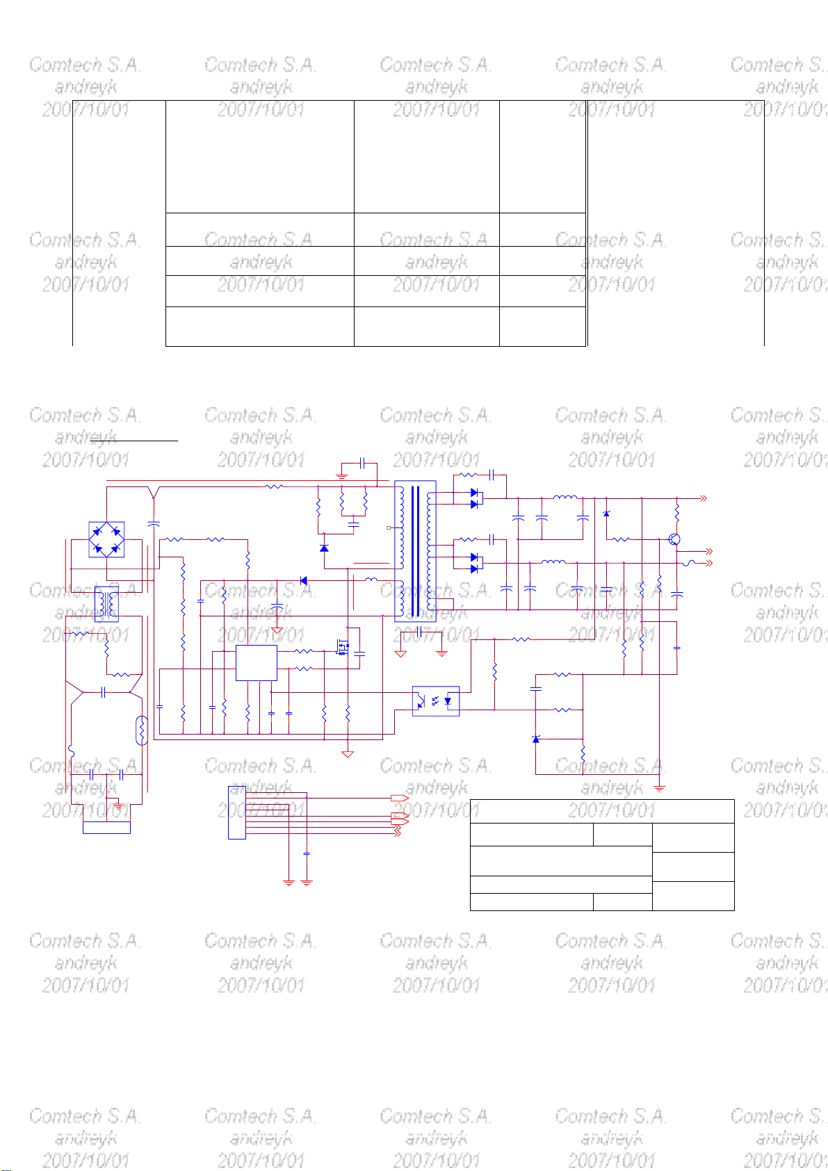
5.1. Block diagram
Power Board
C805
D801
BL4-06
2
AC 264V RMS
4 1
3 2
R801
330K
AC 264V RMS
0.47/275V
F801
2A/250V
C801
1000p/400V
1 2 3
L
AC_SKT
1
4
R803 330K
C803
P801
-+
R802
330K
RT801
NTC 5R
C802
1000p/400V
L801
20mH
DC 380V Max.
C804
+
100u/450V
3
AC 264V RMS
R810
3M
R811
3M
C811
2.2u/50V
AC 264V RMS
N
R806
150K
R809
3M
R812
330K 1%
R807
150K
C810
0.1/50V
R818
1M 1%
OVP
BNO
120K 1%
C812
100P/50V
CN801
TO SCALER BD C N101
8
1
R819
1
2
3
4
5
6
7
8
90mm 8P
VCC
7
LD7522
IC802
345
(-)LATCH
R833
4K7
R808
150K
GND
+
6
OUT
CS
2
COMP
C813
1000p/50V
R805
0.24R 1/ 2W
R804
68K 2W
1N4007
D804
C807
10u/25V
R816
1K
C814
100p/50V
R813
10R
C827
0.1/50V
Q804
AP2761I
2200p/400V
R834
68
D802
MUR1100ERL
23
1
R814
10K
R835
68
C806
4700p/400V
DC 650V Max
FB801
120Ω 3A
DC 650V Max
C808
47p/1KV
R815
0R49 2W
1
2
3
5
6
T801
SPW-0xx
3
VOLUME
MUTE
C828
2200p/400V
LTV817M
IC801
VCC5V
BKLT-EN 2
VBRI 2
Power saving
C815
R827
1000p/500V
10
1
11
12
7
8
9
10
3
R828
10
1
3
D805
SRF5-04C T
14
2
2
D803
SP10100C
C816
1000p/500V
2
C820
470u/25V
+
R832
270 1%
R820
3K 1%
IC803
TLV431ALP
+
C817
680u/25V
+
C823
470u/25V
C
A
InnoLux
Document Number : SIZE :
TITLE :
POWER SUPPLY
C818
680u/25V
+
5uH
L803
R821
1K 1%
C821
0.022/100V
R826
NC
R
5uH
L802
C819
470u/25V
C824
47u/25V
+
+
R824
3K3 1%
E900W
ZD801
9V1
R830
200
C822
0.1/50V
R822
5K1 1%
at each modes
+14V
R831
100Ω 1W
2
Q801
3
2PC1815GR
+5V
1
F802
4A/125V
+
C829
NC
C826
NC
VCC5V
R825 51K 1%
R829 10K
R823
0 1%
A4
APPRO BY :
CHECK BY :
26
DATE :
SHEET OF
2007-03-08
Rev :
V0142
DRAWN BY :
Page 2
E900WA Service Manual
IF Board
27
Page 3

E900WA Service Manual
28
Page 4

E900WA Service Manual
5.2 Circuit operation theory
5.2.1. Electronic Circuit Theory
(A) Switching Mode Power Supply theory
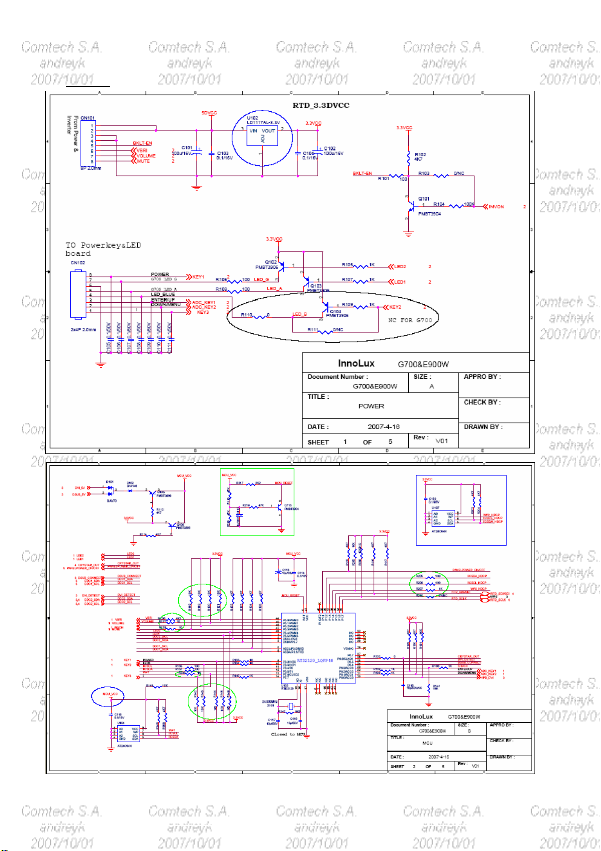
2.1 . AC Current Input Circuit
P801 is a connector for connecting AC Power. F801 is a fuse to protect all the circuit. AC input voltage is from
90V to 264V. R801 and R802 joined between two inputting main circuit to prevent man from shock. L801 is
used to clear up low frequency wave. C801 and C802 are used to discharge the waves that L801 produced.
High frequency waves are damped by C801 and C802. D801 is a rectifier which composed of 4 build-in diodes,
it inverts AC to DC.
2.2 High Voltage to Low Voltage Control Circuit
C804 is used to smooth the waveform from rectifier. IC802 is a highly integrated PWM controller, which control
the power MOSFET Q804. When rectified DC high voltage is applied to the DRAIN pin during start-up, the
MOSFET is off initially, when the voltage VCC reaches the threshold level 11V,IC 802 start up and create a
PWM signal to control the power MOSFET, then energy is transferred to secondary terminal through the
transformer T801,the auxiliary voltage 15V and the output voltage 5V/14V be created ,the auxiliary voltage
supply a continue current to IC802,the level of output voltage is feedback to FB pin of IC802 through IC801 and
IC801 witch control the duty of the PWM signal, then all the convert circuit go to a stable operating station.
29
 Loading...