

Page 1
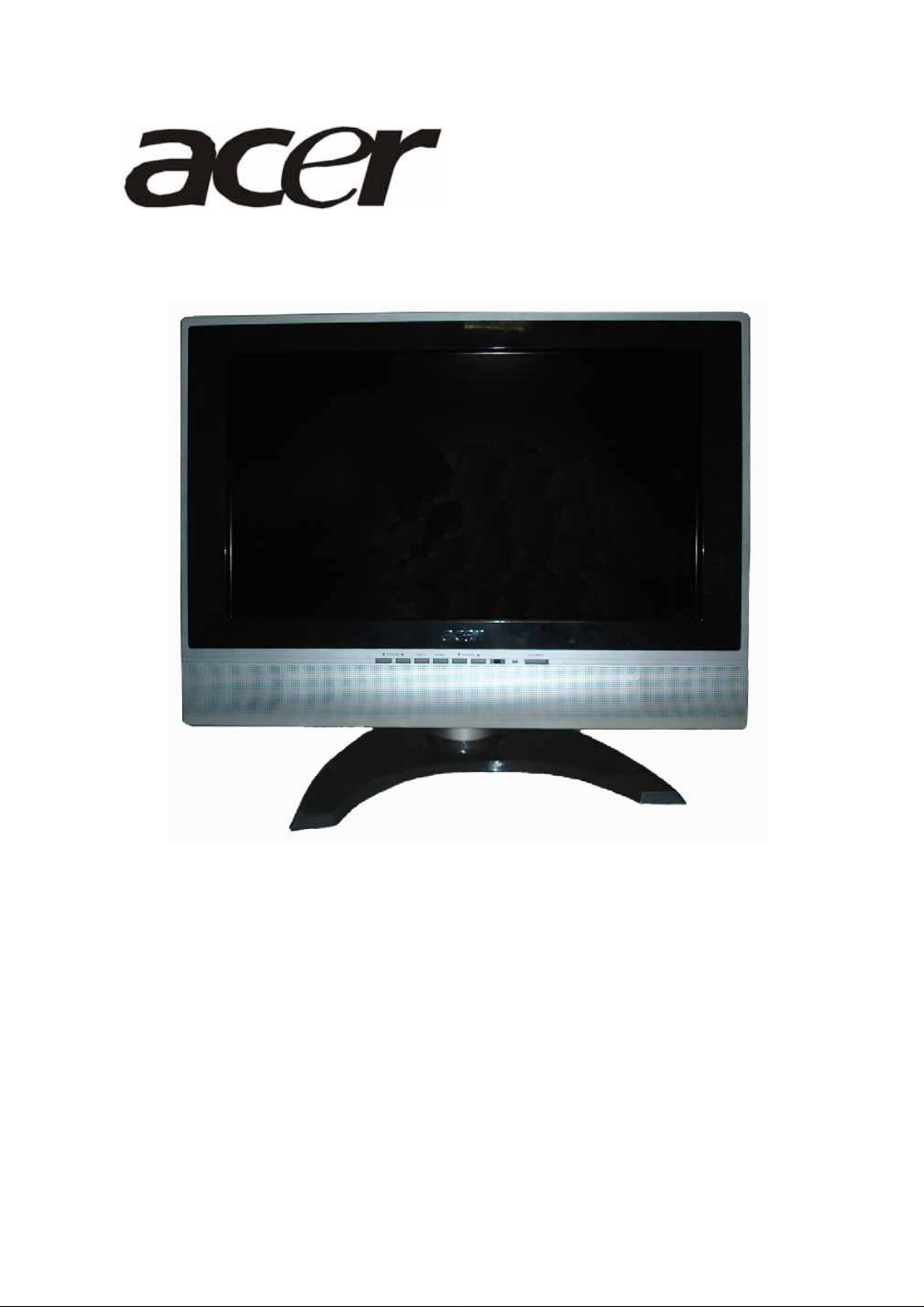
Acer AT2010
Service Guide
1
Page 2
No.
1
Service Guide Version and Revision
Version
A00
Release Date
Mar-24-2006
Revision
Original release
2
Page 3
Copyright
Copyright 2003 Acer Technology Corp.
All rights reserved.
This manual may not, in whole or in part, be copied, photocopied, reproduced, translated, or converted to any
electronic machine readable form without prior written permission of Acer Technology Corp.
ACER AT2010 Service Manual.
Printed in Fujian.
Disclaimer
The information in this guide is s ubj ec t to c hang e without notice. Acer Incorporated makes no representations
or warranties, either expressed or implied, with respect to the contents hereof and specifically disclaims any
warranties of merchantability or fitness for any particular purpose. Any Acer Incorporated software described
in this manual is sold or licensed "as is". Should the programs prove defective following their purchase, the
buyer (and not Acer Incorporated, its distributor, or its dealer) assumes the entire cost of all necessary
servicing, repair, and any incidental or consequential damages resulting from any defect in the software.
Acer is a registered trademark of Acer Corporation.
Intel is a registered trademark of Intel Corporation.
Pentium and Pentium II/III are trademarks of Intel Corporation.
Other brand and product names are trademarks and/or registered trademarks of their respective holders.
Trademarks
All other trademarks are property of their respective owners.
Conventions
The following conventions are used in this manual:
Screen messages Denotes actual messages that appear on screen.
NOTE Gives bits and pieces of additional information related to the current topic.
WARNING Alerts you to any damage that might result from doing or not doing specific
actions.
CAUTION Gives precautionary measures to avoid possible hardware or software
problems.
IMPORTANT Remind you to do specific actions relevant to the accomplishment of
procedures.
Preface
Before using this information and the product it supports, please read the following general information.
1. This Service Guide provides you with all technical information relating to the BASIC CONFIGURATION
decided for Acer's "global" product offering. To better fit local market requirements and enhance product
competitiveness, your regional office may have decided to extend the functionality of a machine (e.g.
add-on card, modem, or extra memory capability). These LOCALIZED FEATURES will NOT be covered in
this generic service guide. In such cases, please contact your regional offices or the responsible
personnel/channel to provide you with furt her technical details.
3
Page 4

2. Please note WHEN ORDERING FRU PARTS, that you should check the most up-to-date information
available on your regional web or channel. If, for whatever reason, a part number change is made, it will not
be noted in the printed Service Guide. For ACER-AUTHORIZED SERVICE PROVIDERS, your Acer office
may have a DIFFERENT part nu m be r cod e to th os e g ive n in t he FR U list o f this printed Service Guide. You
MUST use the list provided by your regional Acer office to order FRU parts for repair and service of
customer machines.
Warning: (For FCC Certified Models)
Note: This equipment has been tested and found to comply with the limits for a Class B digital device,
pursuant to Part 15 of the FCC Rules. These limits ar e designed to provide reasonable protection against
harmful interference in a residential installation. This equipment generates, uses and can radiate radio
frequency energy, and if not installed and used in accordance with the instructions, may cause harmful
interference to radio communications. However, there is no guarantee that interferen ce will not occur in a
particular installation. If this equipment does cause harmful interference to radio or television reception, which
can be determined by turning the equipment off and on, the user is encouraged to try to correct the
interference by one or more of the following measures:
1. Reorient or relocate the receiving antenna.
2. Increase the separation between the equipment and receiver.
3. Connect the equipment into an outlet on a circuit different from that to which the receiver is connected.
4. Consult the dealer or an experienced radio/TV technician for help.
Notice:
1. The changes or modifications not expressly approved by the party responsible for compliance could void
the user's authority to operate the equipment.
2. Shielded interface cables and AC power cord, if any, must be used in order to comply with the emission
limits.
3. The manufacturer is not responsible for any radio or TV interference caused by unauthorized modification
to this equipment. It is the responsibility of the user to correct such interference.
As ENERGY STAR
®
Partner our company has determined that this product meets the ENERGY STAR
guidelines for energy efficiency.
®
Warning:
To prevent fire or shock hazard, do not expose the monitor to rain or moisture. Dangerous high voltages
are present inside the monitor. Do not open the cabinet. Refer servicing to qualified personnel only.
4
Page 5

Precautions
z
Do not use the monitor near water, e.g. near a bathtub, washbowl, kitchen sink, laundry tub, swimming pool
or in a wet basement.
z Do not place the monitor on an unstable trolley, stand, or table. If the monitor falls, it can injure a person
and cause serious damage to the appliance. Use only a trolley or stand recommended by the manufacturer
or sold with the monitor. If you mount the monitor on a wall or shelf, uses a mounting kit approved by the
manufacturer and follow the kit instructions.
z Slots and openings in the back and bottom of the cabinet are provided for ventilation. To ensure reliable
operation of the monitor and to protect it from o verheating, be sure these openings are not blocked or
covered. Do not place the monitor on a bed, sofa , rug, or similar surface. Do not place the monito r near or
over a radiator or he at register. Do not place the mon itor in a b oo kcas e or ca bi ne t unles s prop er vent ilat ion
is provided.
z The moni tor should be operated only from the type of power source indicate d on the label. If you are not
sure of the type of power supplied to your home, consult your dealer or local power company.
z The monitor is equipped with a three-pronged grounded plug, a plug with a third (grounding) pin. This plug
will fit only into a grounded power outlet as a safety feature. If your outlet does not accommodate the
three-wire plug, have an electrician install the correct outlet, or use an adapter to ground the appliance
safely. Do not defeat the safety purpose of the grounded plug.
z Unplug the unit during a lightning storm or when it will not be used for long periods of time. This will protect
the monitor from damage due to power surges.
z Do not overload power strips and extension cords. Overloading can result in fire or electric shock.
z Never push any object into the slot on the monitor cabinet. It cou ld short circuit parts causing a fire or
electric shock. Never spill liquids on the monitor.
z Do not attempt to service the monitor yourself; opening or removing covers can expose you to dangerous
voltages and other hazards. Please refer all servicing to qualified service personnel
z To ensure satisfactory operation, use the monitor only with UL listed computers which have appropriate
configured receptacles marked between 100 - 240V AC, Min. 5A.
z The wall socket shall be installed near the equipment and shall be eas ily accessible.
Special Notes On LCD TV Monitors
The following symptoms are normal with LCD TV monitor and do not indicate a problem.
Notes
z Due to the nature of the fluorescent light, the screen may flicker during initial use. Turn off the Pow er Switch
and then turn it on again to make sure the flicker disappears.
z You may find slightly uneven brightness on the screen depending on the desktop pattern you use.
z The LCD TV screen has effective pixels of 99.99% or more. It may include blemishes of 0.01% or less such
as a missing pixel or a pixel lit all of the time.
z Due to the nature of the LCD TV screen, an afterimage of the previous screen may remain after switching
the image, when the same image is displayed for hour s. In this case, the screen is recovered slowly by
changing the image or turning off the Power Switch for hours.
5
Page 6
Table Of Contents
Monitor Features
General Specifications ……………………………………… 7
LCD TV Description ……………………………………… 8
Chapter 1
Chapter 2
Chapter 3
Chapter 4 Machine Disassembly
Precautions And Notices ……………………………………… 9
D-SUB PIN Distribution ……………………………………… 10
Factory Preset Display Modes ……………………………………… 11
LCD TV Panel Specification ……………………………………… 12
Panel Features ……………………………………… 12
General Specifications ……………………………………… 12
Mechanical Specifications ……………………………………… 12
Optical Specifications ……………………………………… 13
Connecting Peripherals
Front Panel Controls ……………………………………… 14
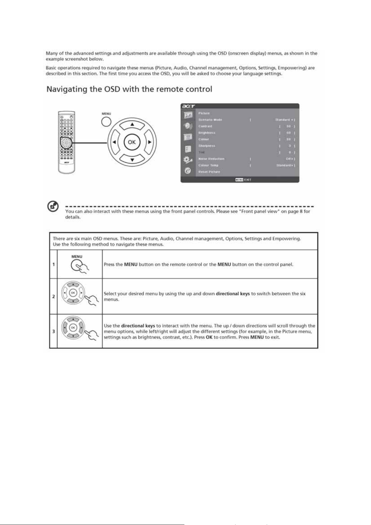
Remote Control & OSD Operating
Instructions
Using The Remote Control ……………………………………… 15
Using The OSD Menus 17
LOGO ……………………………………… 24
……………………………………… 7
……………………………………… 14
……………………………………… 15
……………………………………… 25
Chapter 5 Trouble Shooting
Chapter 6 White-Balance, Luminance Adjustment
FRU (Field Replaceable Unit) List
Chapter 7
Chapter 8 PCB Layout
Chapter 9 Schematic Diagram
Exploded Diagram ……………………………………… 41
EDID Data ……………………………………… 42
……………………………………… 33
……………………………………… 37
……………………………………… 40
……………………………………… 43
……………………………………… 47
6
Page 7
Monitor Features
Chapter 1
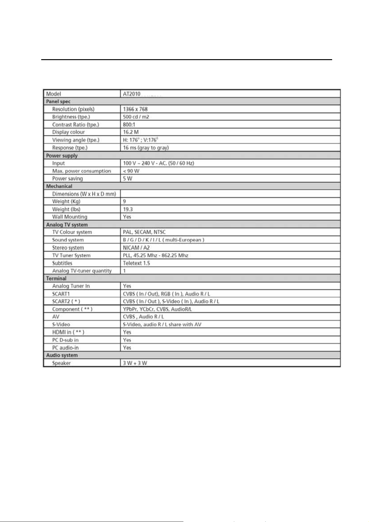
General Specifications
7
Page 8

LCD TV Description
The LCD TV will contain a main board (include audio), an I/O board, a switching power board, a function
keyboard (include an IR Board) and an Ear phone board. The main board and power board will house the flat
panel to control logic I2C bus, DDC, brightness control logic for LCD panel, DC-DC conversion to supply the
appropriate power to the whole board and transmitting TTL level signals into LCD Module to drive the LCD
display circuit.
The inverter board will drive the five CCFLs (Cold Cathode Fluorescent Lamp).
The switching power board will provides the power ON/OFF to control the TV and control LED indicator for
DPMS.
The function keyboard and Remote Control will provide the OSD control signal to the Main Board.
8
Page 9

Precautions And Notices
1-1 Assembly Precaution
(1) Please do not press or scratch LCD panel surface with anything hard. And do not soil LCD panel
surface by touching with bare hands (Polarize film, surface of LCD panel is easy to be flawed)
In the LCD panel, the gap between two glass plates is kept perfectly even to maintain display
characteristic and reliability . If this panel is subject to hard pressing, the following occurs :
(a) Uniform color (b) Orientation of liquid crystal becomes disorder
(2) Please wipe out LCD panel surface with absorbent cotton or soft cloth in case of it being soiled.
(3) Please wipe out drops of adhesive like saliva and water in LCD panel surface immediately.
They might damage to cause panel surface variation a nd color change.
(4) Do not apply any strong mechanical shock to the LCD panel.
1-2 Operating Precaution
(1) Please be sure to unplug the power cord before remove the back-cover. (be sure the power is
turn-off)
(2) Please do not change variable resistance settings in MAIN-BOARD; they are adjusted to the most
suitable value. If they are changed, it might happen LUMINANCE does not satisfy the white
balance spec.
(3) Please consider that LCD backlight takes longer time to become stable of radiation characteristic in
low temperature than in room temperature.
(4) Please pay attention to displaying the same pattern for very long-time. Image might stick on LCD.
1-3 Storage Precaution
(1) When you store LCD for a long time, it is recommended to keep the temperature between -20°C -
60°C without the exposure of sunlight and to keep the humidity less than 85% RH.
(2) Please do not leave the LCD in the environment of high humidity and high temperature such a s
60°C, 95%RH.
(3) Please do not operate the LCD in the environment of abnormal temperature, below 0°C.
1- 4 High Voltage Warning
The high voltage was only generated by Power support part, if carelessly contacted the transformer
on this module, can cause a serious shock.
9
Page 10
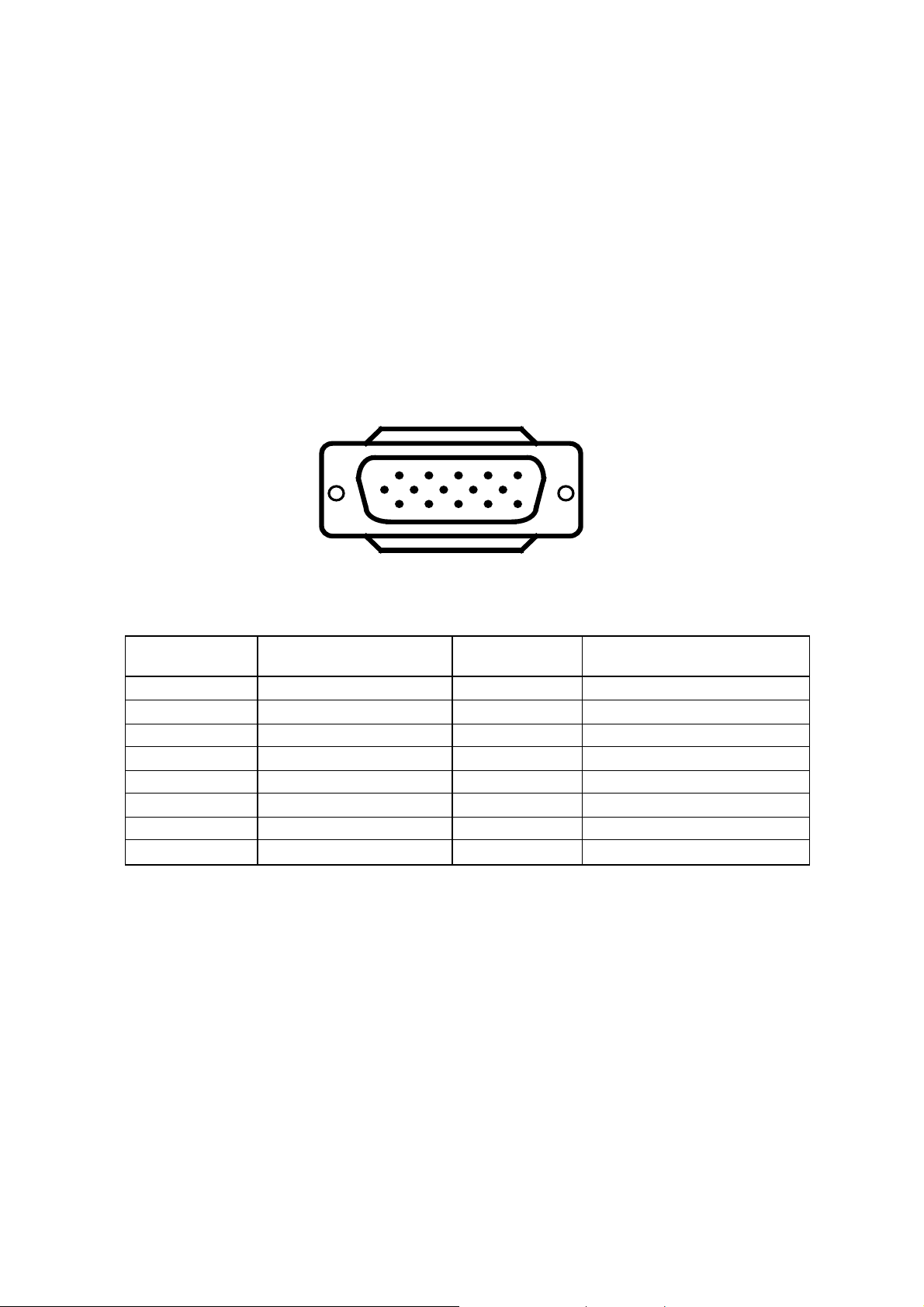
D-SUB PIN Distribution
This procedure gives you instructions for installing and using the LCD TV display.
(1) Position the display on the desired operation and plug the power cord into a convenient AC outlet.
Three-wire power cord must be shielded and is provided as a safety precaution as it connects the chassis
and cabinet to the electrical conduct ground. If the AC outlet in your location does not have provisions for
the grounded type plug, the installer should attach the proper adapter to ensure a safe ground potential.
(2) Connect the 15-pin color display shielded signal cable to your signal system device and lock both screws
on the connector to ensure firm grounding. The connector information is as follow:
1
6
11 15
15 - Pin Color Display Signal Cable
5
10
Pin NO. Description Pin NO. Description
1 Red Video 9 No Pin!
2 Green Video 10 Sync Ground
3 Blue Video 11 Not Used
4 Not Used 12 Serial Data for DDC
5 Ground 13 H-Sync.
6 Red Ground 14 V-Sync.
7 Green Ground 15 Serial Clock for DDC
8 Blue Ground
10
Page 11
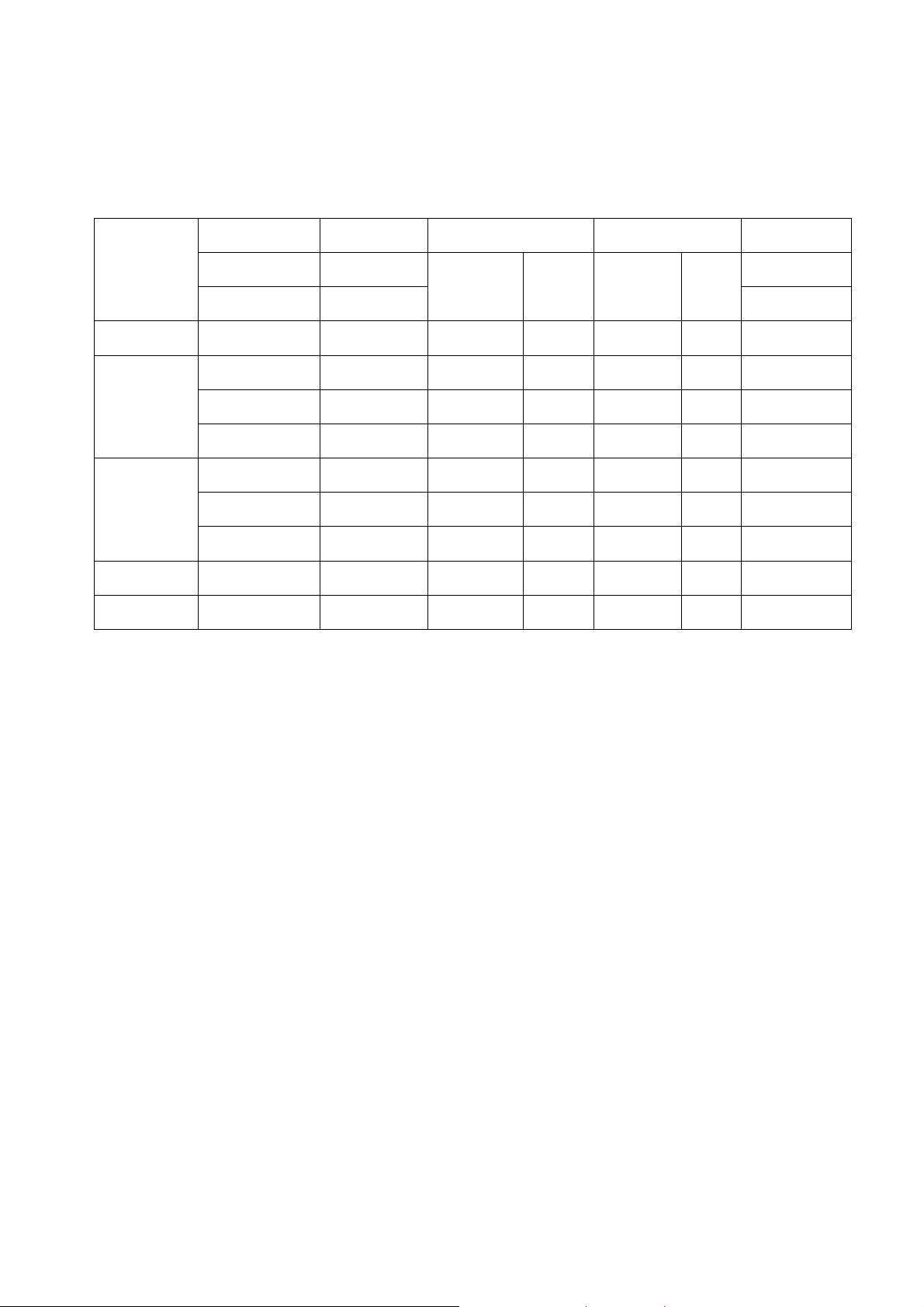
Factory Preset Display Modes:
Analog RGB Signal Timing
Vertical Horizontal Sync Polarity Presence Screen Mode
Dots × Lines
720 ×400 70.1 31.5 NEG POS YES YES YES
640 ×480
800 ×600
1024 × 768 60 48.3 NEG NEG YES YES YES
1280×768 60 47.7 POS POS YES YES YES
Frequency Frequency FULL
Horizontal Vertical Horizontal Vertical
(Hz) (KHz)
59.9 31.5 NEG NEG YES YES YES
72.8 37.9 NEG NEG YES YES YES
75.0 37.5 NEG NEG YES YES YES
60.3 37.9 POS POS YES YES YES
72.2 48.1 POS POS YES YES YES
75.0 46.9 POS POS YES YES YES
(16:9)
11
Page 12
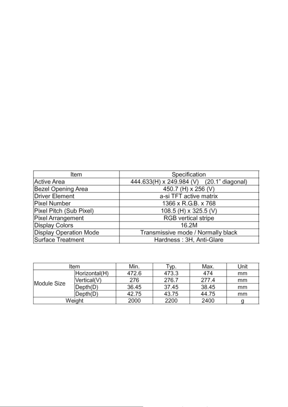
LCD TV Panel Specification
Panel Features
-High brightness (500 nits)
- High contrast ratio (1000:1)
- Fast response time (8ms)
- High color saturation NTSC 75%
- WXGA (1366 x 768 pixels) resolution
- DE (Data Enable) only mode
- LVDS (Low Voltage Differential Signaling) interface
- Optimized response time for 50/60 Hz frame rate
- Ultra wide viewing angle: 176(H)/176(V) (CR>20) Super MVA technology
- 180 degree rotation display option
General Specifications
Mechanical Specification
12
Page 13
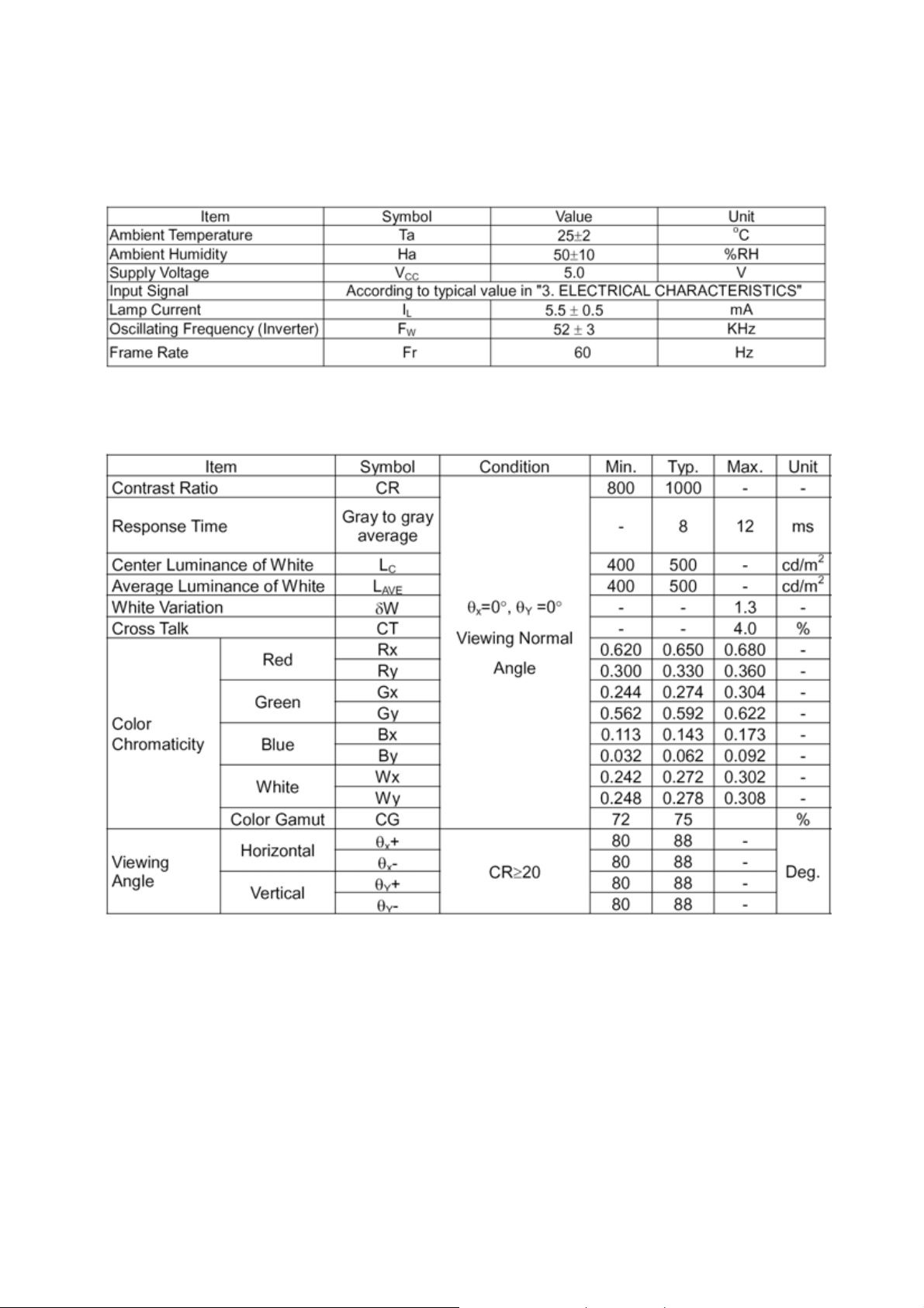
Optical Specifications
Test Conditions
Optical Specifications
13
Page 14
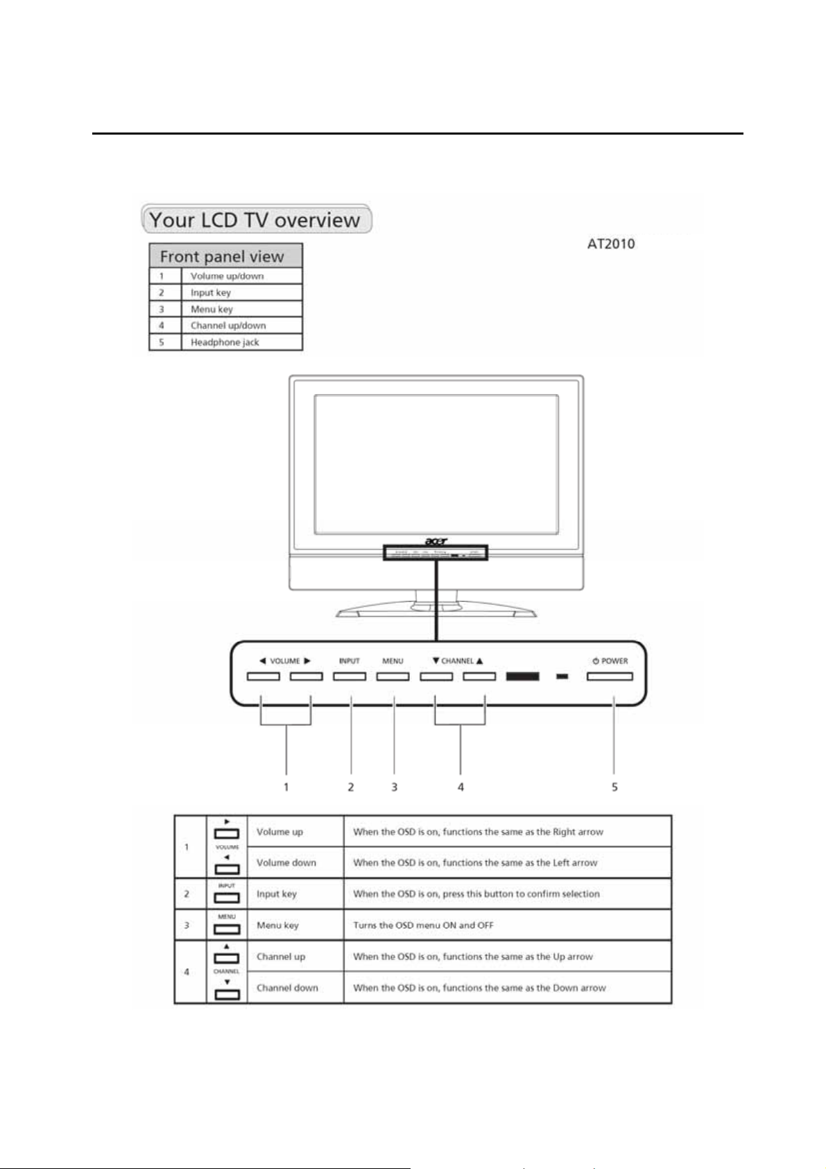
Connecting Peripherals
Chapter 2
Front panel controls
14
Page 15
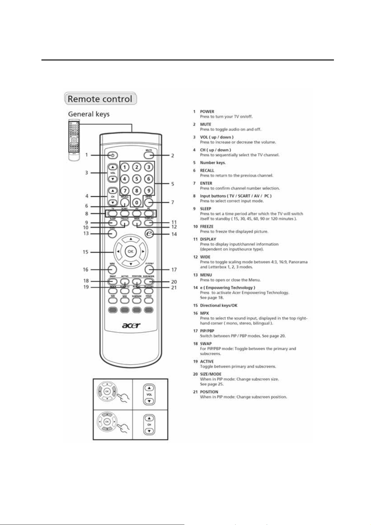
Remote Control & OSD Operating instructions
Chapter 3
Using the Remote Control
15
Page 16
16
Page 17
Using The OSD Menus
17
Page 18
18
Page 19
19
Page 20
20
Page 21

21
Page 22

22
Page 23

23
Page 24

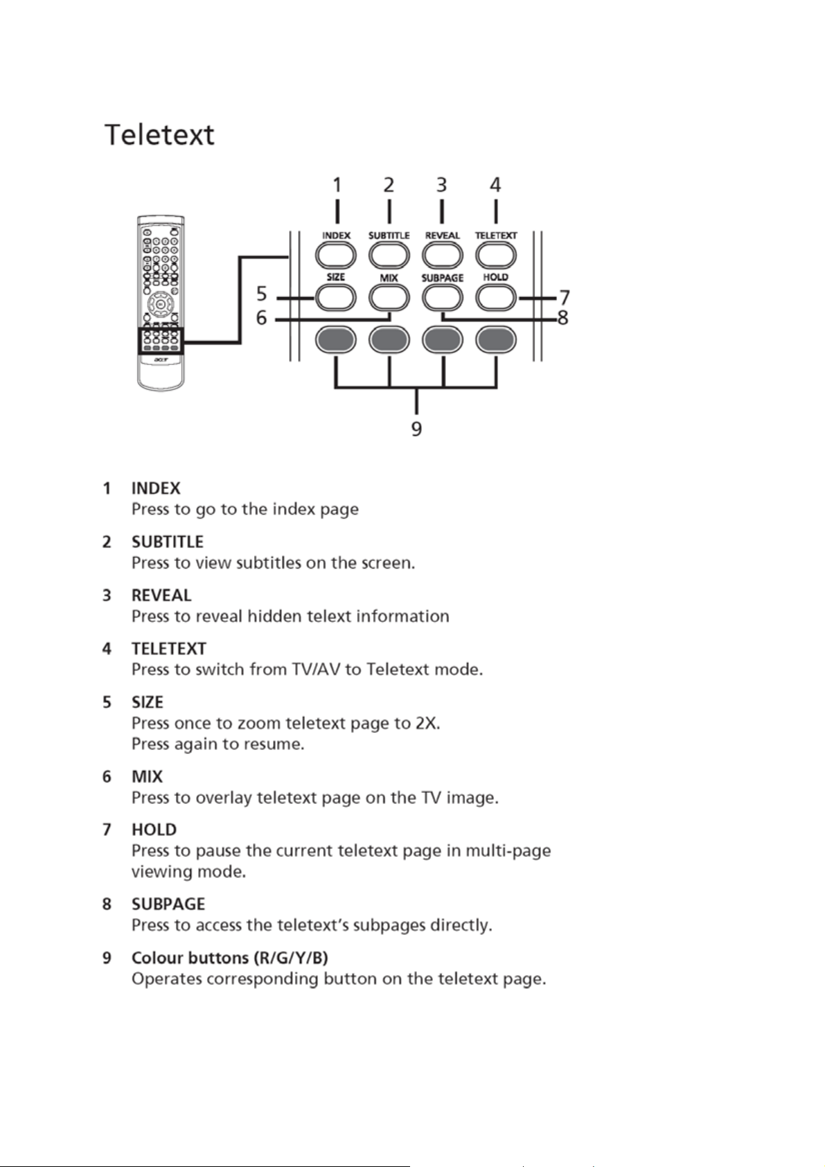
Logo
When the monitor is power on, the LOGO will be showed in the center, and disappear slowly.
How To Optimize The DOS-Mode
Plug And Play
Plug & Play DDC2B Feature
This monitor is equipped with VESA DDC2B capabilities according to the VESA DDC STANDARD. It allows
the monitor to inform the host system of its identity and, depending on the level of DDC used, communicate
additional information about its display capabilities.
The DDC2B is a bi-directional data channel based on the I²C protocol. The host can request EDID
information over the DDC2B channel.
This monitor will appear to be non-functional if there is no video input signal. In order for this
monitor to operate properly, there must be a video input signal.
This monitor meets the Green monitor standards as set by the Video Electronics Standards Association
(VESA) and/or the United States Environmental Protection Agency (EPA) and The Swedish Confederation
Employees (NUTEK). This feature is designed to conserve electrical energy by reducing power
consumption when there is no video-input signal present. When there is no video input signals this monitor,
following a time-out period, will automatically switch to an OFF mode. This reduces the monitor's internal
power supply consumption. After the video input signal is restored, full power is restored and the display is
automatically redrawn. The appearance is similar to a "Screen Saver" feature except the display is
completely off. The display is restored by pressing a key on the keyboard, or clicking the mouse.
Using The Right Power Cord
The accessory power cord for the Northern American region is the wallet plug with NEMA 5-15 style and is
UL listed and CSA labeled. The voltage rating for the power cord shall be 125 volts AC.
Supplied with units intended for connection to power outlet of personal computer: Please use a cord set
consisting of a minimum No. 18 AWG, type SJT or SVT three conductors flexible cord. One end terminates
with a grounding type attachment plug, rated 10A, 250V, CEE-22 male configuration. The other end
terminates with a molded-on type connector body, rated 10A, 250V, having standard CEE-22 female
configuration.
Please note that power supply cord needs to use VDE 0602, 0625, 0821 approval power cord in European
counties.
24
Page 25

Machine Disassembly
Chapter 4
This chapter contains step-by-step procedures on how to disassemble the monitor for
maintenance.
Disassembly Procedure
Disassemble The Base
1. Put the monitor on a clean soft cloth with panel facing to the table. (Fig 1)
2. Take off the cover hinge. (Fig 2-3)
(Fig 1)
(Fig 2)
25
Page 26

(Fig 3)
2. Remove four screws to remove stand base. (Fig 4-5)
(Fig 4)
(Fig
5)
26
Page 27

Disassemble the back cover
1. Remove seven screws to remove back cover. (Fig 6)
( Fig 6 )
Disassemble the shield
1. Remove six screws to remove the shield. The screws are marked in red. (Fig 7)
2. Remove the shield as marked with yellow direction.
(Fig 7)
27
Page 28

2. Remove the shield, then the main board and power board show as below. (Fig 8)
( Fig 8 )
Remove the main board, I/O board and Power Board
1. Remove the twelve screws marked in red to remove power, I/O board and main board. (Fig 9)
2. Remove all the connecting wires for these boards.
( Fig 9)
28
Page 29

Disassemble the Headphone board
1. Remove two screws to headphone board. The screw s are marked in red. (Fig 10-11)
(Fig 10)
(Fig 11)
Disassemble the front panel
1. Remove sixteen screws in red to remove the front panel, (Fig 12-14)
(Fig 12)
29
Page 30

Fig (13)
Fig (14)
Disassemble the speaker
1. Remove eight screws to remove speakers. (Fig 15)
(Fig 15)
30
Page 31

Disassemble the Key board
1. Remove two screws in the keyboard, the screws is marked in red. (Fig 16)
(Fig 16)
Disassemble the Main frame
1. Remove four screws (right and left) to remove metal frame. (Fig 17-18)
Fig (17)
Fig (18)
31
Page 32

2.The panel is disassembled absolutely. Fig (19)
Fig (19)
32
Page 33

p
Trouble Shooting
Chapter 5
Defect Mode Failure Analysis Repair Testing
Abnormal
Missing Line
Bright Dot
Dark Dot
Light Leakage
Mura
Image Sticking
Dot Defect
Check Panel
Brightness Spot
Dot Defect
Particle
No display
Noise
Check Power Board
Check Main board
Check Panel
Check Keyboard
Check Line Connected
Check Main board
Check Panel
Change Power Board
Change Main board
Change Panel
Change Keyboard
Change Main board
Change Panel
Change Wires
Tes
NG
Next Ste
33
Completed
Page 34

Complete
p
A
Noise
Flicker
Abnormal
Gray
R\G\B
Display
Abnormal
Check Single Cable
Check Main board
Check Panel
Check Main board
Check Panel
Check LVD Cable
Check Single Cable
Check Main board
Check Panel
Change Single Cable
Change Main board
Change Panel
Change Main board
Change Panel
Change LVDS Cable
Change Single Cable
Change Main board
Change Panel
Monitor
Shut Down
No signal
Power on
Display
Check Power board
Change Power board
Check Main board
Check Keyboard
Check Single Cable
Check Main board
Check Main board
Change Main board
Change Keyboard
Change Single Cable
Change Main board
Change Main board
Next Ste
Test
A
34
Page 35

A
LED Display
LED Off
Change Keyboard or
Main board or wire
Abnormal
Keyboard
Abnormal
OSD
LED Dark
LED Abnormal
LED Flicker
Check Wires
Change Keyboard or
Main board
Change Keyboard or
Main board or wire
Change Keyboard or
Main board or wire
Change Wires
Check Main board
Check Keyboard
Check Main board
Check LVDS Wire
Change Main board
Change Keyboard
Change Main board
Change LVDS Wire
Next step
Test
Complete
35
Page 36

Key Board
g
OSD is unstable or not workin
Is Key Pad Board connecting normally?
N
Connect Key Pad Board
Y
Is Button Switch normally?
Y
Is Key Pad Board Normally?
Y
Check Main Board
N
N
Replace Button Switch
Replace Key Pad Board
36
Page 37

White-Balance, Luminance Adjustment
Chapter 6
Approximately 30 minutes should be allowed for warm up before proceeding white
balance adjustment.
Before started adjust white balance ,please setting the Chroma-7120
MEM. channel 2 to 12000
channel 5 to 6500
parameter is x = 272 ± 15, y = 278 ± 15, Y = 300± 7 cd/m
= 300± 7 cd/m
15, y = 329 ± 15, Y = 300± 7 cd/m2),
color, ( our 14000 parameter is x = 266 ± 15, y = 270 ± 15, Y = 300 ± 7 cd/m2 ; 12000
2
;8000 parameter is x = 295 ± 15, y = 305 ± 15, Y = 300± 7 cd/m2;6500 parameter is x = 313 ±
MEM. channel 3 to 9300
color,
MEM. channel 4 to 8000
color,
2
;9300 parameter is x = 283 ± 15, y = 297 ± 15, Y
MEM. Channel 1 to 14000
color, and
color,
MEM.
Color Temp. 14000 12000 9300 8000 6500
X 266 272 283 295 313
Y 270 278 297 305 329
Y 300 300 300 300 300
How to setting MEM. channel you can reference to Chroma-7120 user guide or simple use “ SC” key and
NEXT
“
Following is the procedure to do white-balance adjust
” key to modify x, y , Y value and use “ID” key to modify the TEXT description
I. Press Number key 1 Æ 9 Æ 9 Æ 9 will into the factory mode, and press Menu key the
OSD will show menu and a word “F” at LEFT top of Menu.
1. In the factory mode select “COLOR TEMP” may be select the difference color temp.
2. Select SCALER Adjustment:
RG, GG, BG Æ R, G, B Gain adjust.
RB, GB, BB Æ R, G, B Bias adjust.
<Notes: the R, G, B gain use 9 bits, and R, G, B bias use 10 bits to save the value in EEPROM,
so if the R, G, B gain and bias is 255 to 256, the “P0 256”will change to “P10”>
Notes: adjust AV mode the same as PC mode, except the luminance (Pc mode is 350cd/m2,
Av is 420cd/m2).
II. Bias (Low luminance) adjustment:
1. Set the raster pattern (Black pattern with 1024×768) Input.
2. Set the contrast on OSD window to the value=80, Brightness set to “80”
3. Adjust the brightness on OSD until chroma 7120 measurement reach the lowest value.
37
Page 38

III, Gain adjustment:
A. Adjust 14000 color-temperature:
1. Set the Contrast of OSD function to 80 and Adjust Brightness to chroma-7120 Y>350 cd/m2
2. Switch the chroma-7120 to RGB-mode (with press “MODE” button)
3. Switch the MEM.channel to Channel 03 (with up or down arrow on chroma-7120)
4. The LCD-indicator on chroma-7120 will show x = 266 ± 15, y = 270 ± 15, Y = 300 ± 7 cd/m2
5. Adjust the Color (user) Mode: RED on OSD window, until chroma 7120 indicator reached the value R=100
6. Adjust the Color (user) Mode: GREEN on OSD window, until chroma-7120 indicator reached the value G=100
7. Adjust the Color (user) Mode: BLUE on OSD window, until chroma-7120 indicator reached the value B=100
8. Repeat above procedure (Item 5,6,7) until chroma-7120 RGB value meet the tolerance =100±2
9. Switch the chroma-7120 to x, y, Y mode With press “MODE” button to check the color temp is in SPEC. or not.
10. Press MENU to exit the SCALER page and press Save to save the current color temp.
B. Adjust 12000 color-temperature:
1. Set the Contrast of OSD function to 80 and Adjust Brightness to chroma-7120 Y>350 cd/m2
2. Switch the chroma-7120 to RGB-mode (with press “MODE” button )
3. Switch the MEM.channel to Channel 02 ( with up or down arrow on chroma-7120 )
4. The LCD-indicator on chroma-7120 will show x = 272 ± 15, y = 278 ± 15, Y = 300 ± 7 cd/m2
5. Adjust the Color(user)Mode: RED on OSD w i ndow, until chroma 7120 indicator reached the value R=100
6. Adjust the Color (user) Mode: GREEN on OSD window, until chroma-7120 indicator reached the value G=100
7. Adjust the Color(user)Mode: BLUE on OSD w i ndow, until chroma-7120 indicator reached the value B=100
8. Repeat above procedure (item 5,6,7) until chroma-7120 RGB value meet the tolerance =100 ±2
9. Switch the chroma-7120 to x, y, Y mode with press “MODE” button
10. Press MENU to exit the SCALER page and press Save to save the current color temp.
C. Adjust 9300 color-temperature:
1. Set the Contrast of OSD function to 80 and Adjust Brightness to chroma-7120 Y>370 cd/m2
2. Switch the chroma-7120 to RGB-mode (with press “MODE” button)
3. Switch the MEM.channel to Channel 03 (with up or down arrow on chroma-7120)
4. The LCD-indicator on chroma-7120 will show x = 283 ± 15, y = 297 ± 15, Y = 300 ± 7 cd/m2
5. Adjust the Color (user) Mode: RED on OSD window, until chroma 7120 indicator reached the value R=100
6. Adjust the Color (user) Mode: GREEN on OSD window, until chroma-7120 indicator reached the value
G=100
7. Adjust the Color (user) Mode: BLUE on OSD window, until chroma-7120 indicator reached the value
B=100
8. Repeat above procedure ( item 5,6,7) until chroma-7120 RGB value meet the tolerance =100 ± 2
9. Switch the chroma-7120 to XyY mode With press “MODE” button
10. Press MENU to exit the SCALER page and press Save to save the current color temp.
D. Adjust 8000 color-temperature:
1. Set the Contrast of OSD function to 80 and Adjust Brightness to chroma-7120 Y>370 cd/m2
2. Switch the chroma-7120 to RGB-mode (with press “MODE” button)
3. Switch the MEM.channel to Channel 03 (with up or down arrow on chroma-7120 )
4. The LCD-indicator on chroma-7120 will show x = 295 ± 15, y = 305 ± 15, Y = 300 ± 7 cd/m2
38
Page 39

5. Adjust the Color (user) Mode: RED on OSD window, until chroma 7120 indicator reached the value
R=100
6. Adjust the Color (user) Mode: GREEN on OSD window, until chroma-7120 indicator reached the value
G=100
7. Adjust the Color (user) Mode: BLUE on OSD window, until chroma-7120 indicator reached the value
B=100
8. Repeat above procedure (item 5,6,7) until chroma-7120 RGB value meet the tolerance =100 ±2
9. Switch the chroma-7120 to X, y, Y mode with press “MODE” button
10. Press MENU to exit the SCALER page and press Save to save the current color temp.
E. Adjust 6500 color-temperature:
1. Set the Contrast of OSD function to 80 and Adjust Brightness to chroma-7120 Y>370 cd/m2
2. Switch the chroma-7120 to RGB-mode (with press “MODE” button)
3. Switch the MEM.channel to Channel 03 (with up or down arrow on chroma-7120)
4. The LCD-indicator on chroma-7120 will show x = 313 ± 15, y = 329 ± 15, Y = 300 ± 7 cd/m2
5. Adjust the Color (user) Mode: RED on OSD window, until chroma 7120 indicator reached the value
R=100
6. Adjust the Color (user) Mode: GREEN on OSD window, until chroma-7120 indicator reached the value
G=100
7. Adjust the Color (user) Mode: BLUE on OSD window, until chroma-7120 indicator reached the value
B=100
8. Repeat above procedure (item 5,6,7) until chroma-7120 RGB value meet the tolerance =100 ±2
9. Switch the chroma-7120 to X, y, Y mode with press “MODE” button
10. Press MENU to exit the SCALER page and press Save to save the current color temp.
Turn the POWER-button off to on to qu it from factory mode ( in US ER-mode, the OSD w indow location was
placed at middle of screen)
39
Page 40

FRU (Field Replaceable Unit) List
This chapter gives you the FRU (Field Replaceable Unit) listing in global configurations of AT2010.Refer to
this chapter whenever ordering for parts to repair or for RMA (Return Merchandise Authorization).
NOTE:
information available on your regional web or channel (http://aicsl.acer.com.tw/spl/). For whatever reasons
a part number change is made, it will not be noted in the printed Service Guide. For ACER AUTHORIZED
SERVICE PROVIDERS, your Acer office may have a DIFFERENT part number code from those given in
the FRU list of this printed Service Guide. You MUST use the local FRU list provided by your regional Acer
office to order FRU parts for repair and service of customer machines.
NOTE:
regulations on how to dispose it properly, or follow the rules set by your regional Acer office on how to
return it.
Please note WHEN ORDERING FRU PARTS, that you should check the most up-to-date
To scrap or to return the defective parts, you should follow the local government ordinance or
Chapter 7
40
Page 41

Exploded Diagram (Model: AT2010)
Index Part Name Part No. Qty I ndex Part Name Part No. Qty
1 BEZEL PLATE Q34T 5 1 16 RUBBER FOOT 012T 394 3 7
2 REMOTE LENS Q33T 12 1 17 BASE BKT Q15T 12 1 1
3 POWER LENS Q33T 11 1 1 18 BASE Q34T 17 1
4 BEZEL Q34T 16 1 19 STAND M1L1140-6128 1
5 KEY PAD Q33T 10 1 20 HINGE 037T 525 2 1
6 SPEAKER 078T 443 2 21 STAND MID Q33T4836 1
7 KEY BOARD FOR ROHS KEPFA60KB6P 1 22 STAND TOP Q33T4837 1
8 PANEL 750TVMA1WB1 1 23 HINGE BKT 015T6257 1 1
9 MAIN FRAME 015T6254 1 1 24 CLIP CABLE Q33T4832 1
10 TUNER BOARD SMT SMTHJPFA60A8P 1 25 CARD READER 033T4907 1
11 SHIELD-BKT 015T6269 2 1 26 AUDIO BOARD N/A 1
12 MAIN BOARD CBPFAF5BMTATP 1 27 COVER HINGE 034T1656 1
13 POWER BOARD ADPC24100B1P 1 28 REAR COVER 034T1652 1
14 SHIELD MAIN 085T6134 1 1 29 PC PLATE ON TOP 033T6301 1
15 COVER CABLE 034T1655 1
41
Page 42

EDID Data
00 01 02 03 04 05 06 07 08 09 10 11 12 13 14 15
0 : 00 FF FF FF FF FF FF 00 04 72 10 20 0B 95 0D 00
16 : 14 0F 01 03 68 28 1E 78 2A 8E 60 A5 55 44 99 24
32 : 12 49 4B AD C8 00 01 01 01 01 01 01 01 01 01 01
48 : 01 01 01 01 01 01 0E 1F 00 80 51 00 1E 30 40 80
64 : 37 00 BC F9 10 00 00 1C 00 00 00 FF 00 31 31 31
80 : 31 31 31 31 31 31 0A 20 20 20 00 00 00 FD 00 38
96 : 4B 1F 32 08 00 0A 20 20 20 20 20 20 00 00 00 FC
112: 00 41 54 32 30 31 30 0A 20 20 20 20 20 20 00 21
42
Page 43

PCB Layout
Chapter 8
Main Board Layout
43
Page 44

44
Page 45

Power Board
45
Page 46

Headphone Board
46
Page 47

A
r
Schematic Diagram
Main Board
LVDS
ADC
PIP
Pop
COMP
CVBS2
CVBS1
Din
Video Select
SUB Video
SAA7117AE
D-SU
ISP
Select
B
ISP-SW
TX/RX
SD1/SC1
Flash
4MX32
74LVC14
MCU
M30620
SRA
HS/VS
RGB
Select
control
Panel
Scale
Decoder
SVP-EX52
Mode1/Mode2
NJM2244
Decoder
Chapter 9
CH3/CH4
AV1
AV2
S-Video
V1
AV2
CVBS1
NDC700
Audio
Select
Speaker
Ear phone
Subwoofer-Out
Amplifier
MX9704
PT2308
NJW1147
PC
Audio
Decode
SIF
47
74HC405
AV1
AV2
COMP
Page 48

R241
33 1/16W
SCART1_FB
150 OHM
VGAHS7
VGAVS7
1
VGAVS
VGAHS
1 2
150 OHM
3
2
R229
NC
FB23
VGA_SDA_IN
FB26
1 2
VGA_SCL_IN
R239
22 1/16W
VGAHS
VGAVS
C804
100pF
R252 10K 1/16W
R253 10K 1/16W
D108
100 1/16W
BAT54S
5V
C800
0.047uF
C801
0.047uF
3.3V_SB
R230
NC
VGA_HS
VGA_VS
R240
22 1/16W
FB
C805
47pF
8
VGA_SDA
VGA_SCL
0.1uF
R105
5
6
4
8-pin, 300mil DIP with socket
C105
1K 1/16W
32
1
D105
2
3
1
BAT54S
D106
2
3
1
BAT54S
CN108
1617
GG
RxD
C221
0.1uF
U102
VCC
SDA
SCL
GND
24LC21A
I2C Address: 1010 000x
R106
Q105
PMBS3904
1M 1/16W
R848
100K 1/16W
6
11
1
11
7
12
2
12
8
13
3
13
9
14
4
14
10
15
5
15
DB15
U101
1 2
1A 1Y
3 4
2A 2Y
5 6
3A 3Y
9 8
4A 4Y
11 10
74LVC14
5A 5Y
13 12
6A 6Y
GNDVCC
74LVC14
3.3V_SB
7
VCLK
3
NC2
2
NC1
1
NC0
3.3V_SB
FB
C106
0.1uF
R847
33K 1/16W
C802
0.47uF/50V
C803
0.47uF/50V
6
1
7
2
8
3
9
TxD
4
10
5
714
5V_SB
PMBS3906
R846
Q101
R548
R547
D101
MLL4148
75 1/16W
75 1/16W
R242 NC
R243 22 1/16W
R244 NC
R245 22 1/16W
R104 100K 1/16W
D104
3
BAT54C
VGA_HS
C225
0.1uF
D
G
S
5V_SB
R849
33K 1/16W
Q106
PMBS3906
R111 0 1/16W
R110 0 1/16W
R109 0 1/16W
D102
MLL4148
C104
0.1uF
2
1
ZD101
MLL752A
Detect_VGAVS 7
To mcu
Q102
2N7002
R549
D103
MLL4148
75 1/16W
VGA_HSIN 4
VGA_VSIN 4
SC1_FB 4
DET_FB 7
ZD102
MLL752A
Detect_VGAHS 7
Q107
2N7002
VGA_VS
5V_SB
TUNER_OUT
TxD
RxD
VGA_RIN 4
VGA_GIN 4
VGA_BIN 4
R880
22K 1/16W
10uF/16V
C816
R884
18K 1/16W
Audio_L+11
Audio_L-11
Audio_R+11
Audio_R-11
10
CONN
CONN
123
876
123
876
TV_PIP
NC
CN102
CN104
RN11
30K 1/16W
RN12
10K 1/16W
5V
INV_PRO7
BL_ADJ3,7
REMOTE7
R112
3.3V_SB
5V_SB
5V
KEY_AD7
R850 0 1/16W
NC
R851 0 1/16W
+12VP
+5VP
W_ENABLE7
EAR_L11
EAR_R11
5
11
14
3
6
10
13
R103 NC
12V
5V
5V_SB
R107
NC
R113
2.2K 1/16W
R114
0 1/16W
NC
U104
VCCS1A
IN
S1B
S1C
DA
S1D
DB
DC
DD
S2A
S2B
S2C
EN
S2D
GND
PI5V330Q
L107 150 OHM
L108 150 OHM
6
7
8
120 OHM(8P4R)
LP108
7
6
5
120 OHM(8P4R)
LP107
5V
162
1
4
7
9
12
C818
15
8
47uF/16V
C107
0.1uF
0.001uF
R102
NC
C111
C110
22pF
22pF
45
3
2
1
L109 150 OHM
18
2
3
4
C114100pF
AOC (Top Victory) Electronics Co., Ltd.
Title
Size Document Number Rev
B
Date: Sheet
Saturday, March 11, 2006
I/O
TV2065W-4E
+
C1150.1uF
Y_IN1
C_IN1
C819
0.1uF
C131
LOW:INPUT1
HIGH:INPUT2
SVIDEO_SW 7
Y_IN1 4
C_IN1 4
C108
0.1uF
1
2
3
4
5
6
7
8
9
10
C132
0.001uF
C138
C1010.1uF
C1160.1uF
of
2
CN101
6
5
4
3
2
1
0.001uF
CONN
CN105
CONN
1
2
3
4
5
6
7
8
14
CN107
CONN
1
U103 74HC4052D
13
3
SC1_FN7, 10
SC2_FN7, 10
SC17,8
SD17,8
COMP_Y4
COMP_PB4
COMP_PR4
SCART1_G4,10
SCART1_B4,10
SCART1_R4,10
SCART1_FB10
5V
+
32
PMBS3904
1
X
Y
VDD
GND
8
5V
12V_T
Q103
R882
75 1/16W
R885
470 1/16W
X0
X1
X2
X3
Y0
Y1
Y2
Y3
A
B
EN
VEE
10uF/16V
REMOTE
C102
12
14
15
11
1
5
2
4
10
9
6
7
16
+
L110
120 OHM
TX 7
SC1 7,8
RX 7
SD1 7,8
ISP_SW 7
5V_SB
CN106
2
4
6
8
10
12
14
16
18
20
22
24
26
28
30
32
34
36
CONN
4
TV_MAIN
TUNER_OUT
EMI
L101 150 OHM
L102 150 OHM
L104 150 OHM
L105 150 OHM
SVIDEO_Y
SVIDEO_C
SCART2_CVBS
SCART2_C
1
3
5
7
9
11
13
15
17
19
21
23
25
27
29
31
33
35
22K 1/16W
10uF/16V
C817
18K 1/16W
R881
+
R886
5V
1
TUNER_OUT
SVIDEO_Y
SVIDEO_C
C826 10uF/16V
C827 2.2uF/16V
C828 10uF/16V
C829 2.2uF/16V
PC_R_I 11
PC_L_I 11
R_OUT 11
L_OUT 11
SCART1_CVBS 10
SCART2_CVBS 4,10
SCART2_C 4,10
AV_1 10
CVBS_SEL 4
32
Q104
PMBS3904
R883
75 1/16W
R887
470 1/16W
C134
C133
470pF
470pF
C136
C135
470pF
470pF
3
2
1
2
1
L111
120 OHM
3.3V_SB
4
5
4
5
48
Page 49

5V
C312
0.1uF
VDDMQ
C313
0.1uF
C314
0.1uF
C315
0.1uF
C316
0.1uF
C317
0.1uF
C318
0.1uF
C319
0.1uF
R15
10K 1/16W
MPUGPIO0
INPUT
MPUGPIO1
0
0
1
1
VDDMQ
MPUGPIO0
VDDMQ
CS1#
C328
0.1uF
139
137
141
VSSR
VDDR
RAS#
CAS#
138
192
MVREF
140
MPUGPIO1
193
191
NC
MPUGPIO0
MPUGPIO1
MPUCS0N
TESTMODE
190
MPUGPIO4
189
188
MPUGPIO2
MPUGPIO3
MPUGPIO4
17
P_17
18
FLD/IO
SDA_EX
16
SDA
SCL_EX
14
SCL
203
A_D7
202
A_D6
201
A_D5
200
A_D4
197
A_D3
196
A_D2
195
A_D1
194
A_D0
216
RD#
217
WR#
218
ALE
219
220
INT#
15
V5SF
12
13
RESET
147
BA1
145
BA0
144
CLKE
142
WE#
MVREF 5
CAS# 5
RAS# 5
CS0# 5
MCLK0# 5
MCLK0 5
EX-PWM
RN24 100 1/16W
1
2
3
4
1
2
3
4
RN25 100 1/16W
RD_EMU 7
WR_EMU 7
ALE_EMU 7
INT# 7
BA1 5
BA0 5
CLKE 5
WE# 5
8
7
6
5
8
7
6
5
R12
1K 1/16W
CS 7
R6
10 1/16W
MPUCS0N
AD7
AD6
AD5
AD4
AD3
AD2
AD1
AD0
VDDM
R1
1K 1/16W
C3
10uF/16V
RST_H 7
R11
10K 1/16W
175
VDDM
VDDM
DQS0
82
DQS0
C325
0.1uF
171
VDDM
DQS1
100
DQS1
C326
C327
0.1uF
0.1uF
161
153
136
134
124
119
103958577173
VDDM
VDDM
VDDM
VDDM
VDDM
VDDM
99
VDDM
VDDM
VDDM
VDDM
VDDM
VSSM
157
VDDM
VDDM
SVP-EX [256]
(1 of 2)
DQS2
DQS3
MA11
MA10
MA9
MA8
MA7
MA6
MA5
MA4
MA3
MA2
MA1
MA0
156
174
109
111
112
114
115
117
118
120
122
123
125
126
DQS2
DQS3
MA9
MA11
MA7
MA8
MA10
MA6
MA4
MA5
MA3
100 1/16W
RN58
MA0
MA1
MA2
176
169
VSSM
155
VSSM
VSSM
ADDR7
213
5
4
MCU_A7
158
212
MCU_A6
151
132
VSSM
VSSM
ADDR5
ADDR6
210
211
876
123
MCU_A4
MCU_A5
129
121
VSSM
VSSM
ADDR3
ADDR4
208
209
5
4
MCU_A2
MCU_A3
116
105
VSSM
VSSM
ADDR1
ADDR2
206
207
876
123
MCU_A1
MCU_A0
10187838180
98
VSSM
VSSM
VSSM
ADDR0
RN59
100 1/16W
130
VSSM
VSSM
VSSM
MCK0
MCK0#
CS0#
131
133
135
MCU_A[0..7] 7,14
C320
C321
0.1uF
C322
0.1uF
MD0
MD1
MD2
MD3
MD4
MD5
MD6
MD7
MD8
MD9
MD10
MD11
MD12
MD13
MD14
MD15
MD16
MD17
MD18
MD19
MD20
MD21
MD22
MD23
MD24
MD25
MD26
MD27
MD28
MD29
MD30
MD31
DQM0
DQM1
DQM2
DQM3
0.1uF
MD[0..31]5
DQM[0..3]5
C323
0.1uF
73
75
76
78
84
86
88
90
91
93
94
96
102
104
106
108
148
150
152
154
160
162
163
165
166
168
170
172
178
180
181
183
79
97
159
177
SVP-EX_52
DQS[0..3]5
U401A
MD0
MD1
MD2
MD3
MD4
MD5
MD6
MD7
MD8
MD9
MD10
MD11
MD12
MD13
MD14
MD15
MD16
MD17
MD18
MD19
MD20
MD21
MD22
MD23
MD24
MD25
MD26
MD27
MD28
MD29
MD30
MD31
DQM0
DQM1
DQM2
DQM3
MA[0..11]5
C324
0.1uF
VDDMQ
179
*CS1N is not a input or output pin
CS1N=0: SVP-EX CPU access enabled
CS1N=1:SVP-EX CPU access disabled
5V
R2
4.7K 1/16W
Q401
1
PMBS3904
2 3
100uF/16V
AD[0..7] 7,14
R13
4.7K 1/16W
Connector for Amtel AT76C112 Video Output
R5
0 1/16W
C1
MPUGPIO0
0
1
0
1
+
C2
0.1uF
C4
68pF
C6
0.1uF
MPUCS0N
BL_ADJ 2,7
R9 68 1/16W
R10 68 1/16W
C5
68pF
5V_SB
0
1
1
1
AOC (Top Victory) Electronics Co., Ltd.
Title
Size Document Number Rev
B
Date: Sheet
Saturday, March 11, 2006
MPUCS0N
OUTPUT
*CS1N
1
0
1
1
3V_SDA 8,10
3V_SCL 8,10
VD3_3
R17
10K 1/16W
SVP-EX256_1
TV2065W-4E
MPUGPIO2
1
1
0
1
I2C Address:
7E/7F
I2C Address:
7C/7D
Not
Populated
MPUGPIO3
1
1
1
0
MPUGPIO4
R20
0 1/16W
MPU has
Data/Address
multiplex
MPU has
separated
Address/Data
1
of
3
14
49
Page 50

DIN[0..23]8,10
VL1_8
VD1_8
VD1_8
FB11
1 2
30 OHM
FB12
1 2
30 OHM
CLK_2EX8,10
DIN23
DIN22
DIN21
DIN20
SVP-EX_52
20pF
C36
10uF/16V
C43
10uF/16V
MLF1
PLF2
C25
69
70
71
72
3
6
9
67
89
107
113
143
149
167
184
198
214
251
8
68
74
92
110
146
164
182
185
199
215
250
U401B
DIN23
DIN22
DIN21
DIN20
MLF1
PLF2
VDDC
VDDC
VDDC
VDDC
VDDC
VDDC
VDDC
VDDC
VDDC
VDDC
VDDC
VDDC
VSSC
VSSC
VSSC
VSSC
VSSC
VSSC
VSSC
VSSC
VSSC
VSSC
VSSC
VSSC
X401
14.318MHz
C37
0.1uF
C44
0.1uF
C51
0.1uF
C57
0.1uF
0.1uF
C52
C58
0.1uF
CLK_2EX
DIN1
DIN2
DIN0
P_62
P_63
P_64
XTALO
XTALI
1
256
C26
20pF
C35
C42 0.0027uF
C53
0.1uF
C59
0.1uF
DIN4
DIN6
DIN8
DIN5
DIN7
DIN3
DIN9
CLK_2EX
P_55
P_56
P_57
P_58
P_59
P_60
P_61
DIN15
DIN14
DIN13
DIN12
DIN10
DIN11
P_51
P_50
P_47
P_48
P_49
P_50
P_51
P_52
P_53
P_54
SVP-EX [256]
(2 of 2)
PAVSS
PDVSS
AVSS_ADC1
AVSS3_BG_ASS
AVSS_ADC2
AVSS_ADC3
VSSH
VSSL
PAVSS2
PAVSS1
754
PAVSS1
PAVSS2
0.0027uF
C54
0.1uF
C60
0.1uF
255
253
PAVSS
PDVSS
PAVDD1
PAVSS1
PAVDD2
PAVSS2
MLF1
239
AVSS_ADC1
PLF2
C55
0.1uF
C61
0.1uF
AVSS_ADC2
VSSH
VSSH
VSSH
235
228
222
205
127
20
66
187
VSSL
AVSS_ADC3
AVSS3_BG_ASS
VSSH
VDDL
VSSL
PDVDD
PDVSS
PAVDD
C56
0.1uF
PAVSS
VDDH
C62
0.1uF
VSSH
DIN17
DIN18
DIN16
P_43
P_44
P_45
P_46
PAVDD
PAVDD2
PAVDD1
254
2
PAVDD
PAVDD1
PAVDD2
C29
0.1uF
C38
0.1uF
C45
0.1uF
C49
0.1uF
R410 NC
VD3_3
R509
1K 1/16W
DIN19
P_41
P_40
P_41
P_42
PDVDD
AVDD_ADC1
252
238
227
AVDD_ADC1
AVDD_ADC2
PDVDD
P_39
P_37
P_38
374041
38394243444546474849505152535455565758596061626364
P_37
P_40
P_38
P_39
AVDD3_AVSP2
AVDD_ADC2
AVDD_ADC3
234
221
AVDD_ADC3
AVDD3_AVSP2
FB1
1 2
150 OHM
C30
10uF/16V
FB4
1 2
150 OHM
C39
10uF/16V
FB7
1 2
150 OHM
C46
10uF/16V
FB9
1 2
C50
150 OHM
10uF/16V
P_37
TXOUT0- 6
P_36
TXOUT0+ 6
P_35
TXOUT1- 6
P_34
TXOUT1+ 6
P_31
TXOUT2- 6
P_30
TXOUT2+ 6
P_29
TXCLK- 6
P_28
TXCLK+ 6
P_27
TXOUT3- 6
P_26
TXOUT3+ 6
P_33
P_34
P_36
P_32
P_35
P_33
P_34
P_35
P_36
VDDH
VDDH
VDDH
VDDH
204
128
19
65
186
VDDL
VDDH
EX3V3_SB
VD1_8
VL1_8
VL1_8
VD3_3
P_32
VDDL
P_24
P_29
P_25
P_26
P_30
P_28
P_27
P_31
24252627282930313233343536
P_24
P_25
P_26
P_27
P_28
P_29
P_30
P_31
DE
V
H
AIN_HS
AIN_VS
PR_R1
Y_G1
PB_B1
PR_R2
Y_G2
PB_B2
CVBS_OUTP
CVBS_OUTN
CVBS1
CVBS2
CVBS3
C
AIN_N1
AIN_N2
AIN_N3
VREFP_1
VREFN_1
VREFP_2
VREFN_2
VREFP_3
VREFN_3
241
240
230
229
224
223
VREFN_3
VREFP_3
VREFN_2
VREFP_2
VREFN_1
VREFP_1
AVDD_ADC1
C31
0.1uF
AVSS_ADC1
AVDD_ADC2
C40
0.1uF
AVSS_ADC2
AVDD_ADC3
C47
0.1uF
AVSS_ADC3
AVDD3_AVSP2
C63
0.1uF
AVSS3_BG_ASS
EX3V3_SB
C311
0.1uF
VSSH
Place 75 ohm resistors
close to SVP-EX
R23 0 1/16W
R24 NC
23
22
DVS_2EX 8,10
21
DHS_2EX 8,10
10
VGA_HSIN 2
11
VGA_VSIN 2
PR_R1
225
Y_G1
246
PB_B1
232
PR_R2
226
Y_G2
248
PB_B2
233
236
237
CVBS1
242
CVBS2
243
CVBS3
244
C
231
AIN_N1
245
AIN_N2
247
AIN_N3
249
L402 2.2uH
C32
10uF/16V
L403 2.2uH
C41
10uF/16V
L404 2.2uH
C48
10uF/16V
FB10
1 2
150 OHM
C64
10uF/16V
L401 2.2uH
VD3_3
3.3V_SB
VA1_8
VA1_8
VA1_8
SC1_FB 2
DE_2EX 8
0.1uF
C19
P_50
C69
0.1uF
P_51
CVBS2
CVBS1
CVBS3
C
C16
NC
AVSS_ADC1
VD3_3
C7 0.1uF
C9 0.1uF
C11 0.1uF
C13 0.1uF
C20
0.1uF
VD1_8
P_40
C72
0.1uF
P_41
CVBS_SEL 2
R21
NC
75 1/16W
TV_MAIN 2
R25
NC
75 1/16W
Y_IN1
Y_IN1 2
R27
NC
75 1/16W
C_IN1
R29
NC
75 1/16W
C21
0.1uF
P_38
P_33
P_24
P_32
P_25
C_IN1 2
C17
NC
AVSS_ADC2
C70
0.1uF
VD3_3
C71
0.1uF
Y_G1
PB_B1
PR_R1
C22
0.1uF
C8 0.1uF
C10 0.1uF
C12 0.1uF
C23
0.1uF
COMP_Y 2
R22
NC
75 1/16W
COMP_PB 2
R26
NC
75 1/16W
COMP_PR 2
R28
NC
75 1/16W
C18
NC
AVSS_ADC3
C24
0.1uF
Y_G2
PB_B2
PR_R2
AOC (Top Victory) Electronics Co., Ltd.
Title
Size Document Number Rev
Custom
Date: Sheet
Saturday, March 11, 2006
SVP-EX256_2
TV2065W-4E
C14 0.1uF
C15 0.1uF
C27 0.1uF
VGA_GIN 2
R30
NC
75 1/16W
VGA_BIN 2
R31
NC
75 1/16W
VGA_RIN 2
R32
NC
75 1/16W
4
1
14
of
50
Page 51

Test pads for DDR
MCLK0
DDQS0
DQM0
DQ23
CAS#
RAS#
CS0#
WE#
TP7
TP_T_C30
TP8
TP_T_C30
TP9
TP_T_C30
TP10
TP_T_C30
TP11
TP_T_C30
TP12
TP_T_C30
TP13
TP_T_C30
TP31
TP_T_C30
TP14
TP_T_C30
TP15
TP_T_C30
TP16
TP_T_C30
MA[0..11]3
DQ0
DQ1
DQ2
DQ3
DQ4
DQ5
DQ6
DQ7
DQ16
DQ17
DQ18
DQ19
DQ20
DQ21
DQ22
DQ23
DQM1
DQM0
DDQS1
DDQS0
U407
C10
C76
0.1uF
A6
B5
A5
A4
B1
C2
C1
D1
E2
E1
F2
F1
H2
H1
J1
J2
A2
G2
A1
A3
A10
C3
C4
C5
C8
C9
D5
D8
E4
E9
F4
F9
G4
G9
H4
J4
H9
J9
VDDMQ
MA11
MA10
MA9
MA3
MA4
MA2
MA7
MA1
MA0
MA6
MA8
MA5
L4
M3
K5L7M10M9M8L8M7M6L5M5M4
A9
VSS
VSS
VSS
VSS
VSS
J6
J7J8D4D6D7
A7A6A5A4A3A2A1
A11
A10
BA1
BA0
A8_AP
4M x 32 DDR
FBGA 144
VSS
VSS
VSS
VSS
VSS
VSS
VSS
VSS
D9
E5
DQ0
DQ1
DQ2
DQ3
DQ4
DQ5
DQ6
DQ7
DQ16
DQ17
DQ18
DQ19
DQ20
DQ21
DQ22
DQ23
DM0
DM2
DQS0
VSSQ
VSSQ
VSSQ
VSSQ
VSSQ
VSSQ
VSSQ
VSSQ
VSSQ
VSSQ
VSSQ
VSSQ
VSSQ
VSSQ
VSSQ
VSSQ
VSSQ
VSSQ
VSSQ
VSSQ
A0
K4K9J5
DDR VDDMQ / VDDM de-caps
C79
C80
C77
0.1uF
C78
0.01uF
0.01uF
0.01uF
C81
0.01uF
M1L1K1
CS#
VSS
RAS#
VSS
K2
CAS#
VSS
C82
0.01uF
WE#
VSS
MCLK0
R124
51 1/16W
R128
51 1/16W
MCLK0#
DDQS0
R123 15 1/16W
DDQS1
R125 15 1/16W
DDQS2
R126 15 1/16W
DDQS3
R127 15 1/16W
RN1 15
DQ23
5
DQ22
6
DQ20
7
DQ21
8
RN2 15
DQ19
5
DQ18
6
DQ17
7
DQ16
8
RN3 15
DQ7
5
DQ6
6
DQ5
7
DQ4
8
RN4 15
DQ3
5
DQ2
6
DQ1
7
DQ0
8
RN5 15
DQ31
5
DQ29
6
DQ30
7
DQ28
8
RN6 15
DQ27
5
DQ26
6
DQ25
7
DQ24
8
RN7 15
DQ15
5
DQ14
6
DQ13
7
DQ12
8
RN8 15
DQ10
5
DQ11
6
DQ8
7
DQ9
8
MEMORY DECOUPLING SCHEME
SVP-EX_4MX32_DDR
Saturday, March 11, 2006
VDDMQ
DQM[0..3] 3
VDDMQ
VDDMQ
C74
0.1uF
C75
0.1uF
R129
1K 1/16W
R130
1K 1/16W
MVREF 3
AOC (Top Victory) Electronics Co., Ltd.
Title
Size Document Number Rev
B
Date: Sheet of
Each MD trace must be equal length.
Each DQS trace must be equal
length.
BA1 3
BA0 3
CS0# 3
RAS# 3
CAS# 3
WE# 3
VSS
L9
VSS
CLKE 3
K8L6B3G3L2M2L3
RFU2
RFU3
NC_L2
NC_B3
NC_G3
VSS
VSS
VSS
H8H7H6H5G8G7G6G5F8F7F6F5E8E7E6
C84
0.0047uF
NC_M2
VDD
K3K6K7
K11
K12
NC_L3
NC_K11
VDD
VDD
K10D3D10C6C7
G10
B10
NC_K12
NC_G10
VDD
VDD
C85
0.1uF
DQ31
NC_B10
DQ30
DQ29
DQ28
DQ27
DQ26
DQ25
DQ24
DQ15
DQ14
DQ13
DQ12
DQ11
DQ10
DQ9
DQ8
DM3
DM1
DQS3
DQS1DQS2
VREFMCL
VDDQ
VDDQ
VDDQ
VDDQ
VDDQ
VDDQ
VDDQ
VDDQ
VDDQ
VDDQ
VDDQ
VDDQ
VDDQ
VDDQ
VDDQ
VDDQ
VDD
VDD
VDDM
A7
B8
A8
A9
B12
C11
C12
D12
E11
E12
F11
F12
H11
H12
J11
J12
A11
G11
A12
G12G1
M12L12
B2
B4
B6
B7
B9
B11
D2
D11
E3
F3
H3
J3
E10
F10
H10
J10
VDD
4Mx32_DDR
VDDM
C86
0.1uF
DQ31
DQ30
DQ29
DQ28
DQ27
DQ26
DQ25
DQ24
DQ15
DQ14
DQ13
DQ12
DQ11
DQ10
DQ9
DQ8
DQM2
DQM3
DDQS2
DDQS3
C87
0.01uF
MVREF
MCLK0
MCLK0#
L10
L11
M11
CK
CK#
CKE
VSS
VSS
VSS
VSS
C83
0.0047uF
MCLK0 3
C73 0.01uF
MCLK0# 3
DQS0
DQS1
DQS2
DQS3
MD0
4
MD1
3
MD2
2
MD3
1
MD4
4
MD5
3
MD6
2
MD7
1
MD8
4
MD9
3
MD10
2
MD11
1
MD12
4
MD13
3
MD14
2
MD15
1
MD16
4
MD17
3
MD18
2
MD19
1
MD20
4
MD21
3
MD22
2
MD23
1
MD24
4
MD25
3
MD26
2
MD27
1
MD28
4
MD29
3
MD30
2
MD31
1
TV2065W-4E
DQS[0..3] 3
MD[0..31] 3
5
1
14
51
Page 52

C137
0.1uF
L115
150 OHM
EMI
P_CLK
L118
150 OHM
P_DATAEN
0 1/16W
VD3_3
R889 100 1/16W
+3.3VT
+3.3VT
+3.3VT
R890
2.2K 1/16W
NC
Q801
PWR_ON7,12
1
PMBS3904
2 3
L801 2.2uH
B5
P_Hs
P_Vs
P_DATAEN
R6
TXOUT0TXOUT0+
TXOUT1TXOUT1+
TXOUT2TXOUT2+
TXCLKTXCLK+
TXOUT3TXOUT3+
P_CLK
R0
+3.3VT
C820
C821
10uF/16V
0.1uF
1
2
3
4
5
6
7
8
9
10
11
12
13
14
15
16
17
18
19
20
21
22
23
24
25
26
27
28 29
C822
C823
0.1uF
0.1uF
U801
RC3
VCC
RD6
RC2
RC4
RC1
GND
RC0
RC5
GND
RC6
RB6
RD0
RD5
LVDS GND
RD4
RA-
VCC
RA+
RB5
RB-
RB4
RB+
RB3
LVDS VCC
GND
LVDS GND
RB2
RC-
RD3
RC+
RD2
RCLK-
VCC
RCLK+
RB1
RD-
RB0
RD+
RA6
LVDS GND
GND
PLL GND
RA5
PLL VCC
RD1
PLL GND
RA4
/PDWN
RA3
CLKOUT
VCC
RA0
RA2
GND RA1
THC63LVDF84A
C824
0.1uF
56
55
54
53
52
51
50
49
48
47
46
45
44
43
42
41
40
39
38
37
36
35
34
33
32
31
30
PVDD12
B4
B3
B2
B1
B7
B6
B0
G5
G4
G3
G7
G6
G2
G1
G0
R5
R7
R4
R3
R2
R1
TXOUT0+4
TXOUT0-4
TXOUT1+4
TXOUT1-4
TXOUT2+4
TXOUT2-4
TXOUT3+4
TXOUT3-4
TXCLK+4
TXCLK-4
TXOUT0+
TXOUT0-
TXOUT1+
TXOUT1-
TXOUT2+
TXOUT2-
TXOUT3+
TXOUT3-
TXCLK+
TXCLK-
P_Hs
P_Vs
R888
50
CP103 22pF
1
8
2
7
3
6
22pF
C825
L800
300 OHM
C807
0.1uF
4 5
1
2
3
4 5
LP100
150 OHM(8P4R)
+
CN800
1
2
3
4
5
6
7
8
9
10
11
12
13
14
15
16
17
18
19
20
8
7
6
CP105
22pF
C806
10uF/16V
678
4 5
R6
R7
PVDD 12
CN103
12345678910111213141516171819202122232425262728293031323334353637383940414243444546474849
CP102
22pF
45
3
6
2
7
1
8
CP104
22pF
CP106
22pF
678
LP101
150 OHM(8P4R)
123
4 5
G5
G7
G6
G4
150 OHM(8P4R)
LP102
4 5
G3
678
G2
G1
LP103
678
123
G0
4 5
B6
B7
150 OHM(8P4R)
CP107
22pF
678
LP105
LP104
150 OHM(8P4R)
123
4 5
123
B2
B0
B5
B1
B4
B3
678
123
123
4 5
R3
R4
R1
R0
R5
R2
150 OHM(8P4R)
45
3
6
2
7
1
8
45
3
6
2
7
1
8
45
3
6
2
7
1
8
52
R802
0 1/16W
CONN
AOC (Top Victory) Electronics Co., Ltd.
Title
Size Document Number Rev
B
Saturday, March 11, 2006
Date: Sheet of
LVDS / TTL
TV2065W-4E
6
14
1
Page 53

SC1_FN2, 10
SC2_FN2, 10
SVIDEO_SW2
AUDIO_SW111
AUDIO_SW211
Detect_VGAHS2
R431 0 1/16W
R432 0 1/16W
CE_REMOTE8
ACER
ISP_SW2
SCDT8
5V-1_CPU
5V-1_CPU
R429
NC
5V-1_CPU
R800 100 1/16W
5V-1_CPU
4.7K 1/16W
R433
R435
R436
R437
KEY_AD2
DET_FB2
R801
100 1/16W
100 1/16W
100 1/16W
100 1/16W
R430
NC
4.7K 1/16W
R807
ZD401
4.7K 1/16W
Detect_VGAVS2
VGAVS2
VGAHS2
RX_INT#8
BL_ADJ2,3
PWR_ON6,12
4.7K 1/16W
RST_7117
R835 100 1/16W
R836 100 1/16W
AD7
AD6
AD5
AD4
AD3
AD2
AD1
AD0
R425 100 1/16W
R427 100 1/16W
E_PAGE
R808
R809
4.7K 1/16W
4.7K 1/16W
R443 220 1/16W
HZ4A2
R444
8.2K 1/16W
R445 1K 1/16W
C355 1000pF
C330 10uF/16V
R821
5V-1_CPU
R833
R452 4.7K 1/16W
4.7K 1/16W
R453
4.7K 1/16W
R454
5V-1_CPU
R810
4.7K 1/16W
C334
100uF/16V
4.7K 1/16W
R822
R829 100 1/16W
R830 100 1/16W NC
R831 100 1/16W NC
R832 100 1/16W
R834
4.7K 1/16W
76
77
78
79
80
81
82
83
84
85
86
87
88
89
90
91
92
93
94
95
96
97
98
99
100
PMBS3906
5V-1_CPU
TP43
A0
4.7K 1/16W
4.7K 1/16W
R826
R828
R827
4.7K 1/16W
7172737475
P1_4
P1_3
P1_7/INT5
P1_6/INT4
P1_5/INT3
P1_2
P1_1
P1_0
P0_7/AN0_7
P0_6/AN0_6
P0_5/AN0_5
P0_4/AN0_4
P0_3/AN0_3
P0_2/AN0_2
P0_1/AN0_1
P0_0/AN0_0
P10_7/AN7
P10_6/AN6
P10_5/AN5
P10_4/AN4
P10_3/AN3
P10_2/AN2
P10_1/AN1
Avss
P10_0/AN0
Vref
Avcc
P9_7/ADTRG
P9_6
P9_5
P9_3/DA0
P9_4/DA1
P9_2/TB2in
P9_1/TB1in
P9_0/TB0in
2
134679101213
5
5V-1_CPU
Q403
5V-1_CPU
CPU_RST
5V_SB
TP34
TP32
TP36
TP35
TP33
A3
A1
A5
A4
A2
A4
A2
A1
A5
A3
A0
70696867666564
P2_0/A0/D0
P2_1/A1/D1
P2_2/A2/D2
P2_3/A3/D3
P2_4/A4/D4
M30620SPGP
P8_7/Xcin
BYTE
CNVss
P8_6/Xcout
Reset
8
11
R552
4.7K 1/16W
C336
15pF
FB57
150 OHM
C346
0.1uF
AD0
AD1
AD2
AD3
33
AD4
AD5
AD6
AD7
C340
R415 100 1/16W
100 1/16W
R426
R428 100 1/16W
C339
100pF
R449
10K 1/16W
R450 100 1/16W
R451 100 1/16W
AD[0..7] 3,14
VD3_3
RD_EMU 3
1
2 3
C338
100pF
SCLE
SDAE
RD# 14
R414
10K 1/16W
Q402
NC
SC1 2,8
SD1 2,8
R389 0 1/16W
WR_EMU 3
TP40
WR
RST_H 3
RST_7117
RST_711710
100K 1/16W
RST_H3
AOC (Top Victory) Electronics Co., Ltd.
Title
Size Document Number Rev
Custom
Saturday, March 11, 2006
Date: Sheet of
5V-1_CPU
RST_HDMI
R284
5V-1_CPU
R281
4.7K 1/16W
2K 1/16W
VD3_3
R411
1
2
ASM810SEUR-T
MCU_M30620SPGP
TV2065W-4E
R282
4.7K 1/16W
U410
GND
RESET
3.3V_SB
R283
4.7K 1/16W
RST# 8
Q404
1
PMBS3904
2 3
VD3_3
3
VCC
C415
0.1uF
1
7
14
When use W27E040,use R398 and
Q0
Q1
Q2
Q3
Q4
Q5
Q6
Q7
CE#
OE#
VCC
VPP
R400 33 1/16W
R397 33 1/16W
CS1 14
R417 47K 1/16W
NC
R382
Option
U406
VCC
GND
VCLKNC2
NC1
SCL
NC0
SDA
24LC64
R399;R400 and R404 are
Option.
When use W29C040,use R404 and
R400;R398 and R399 are
Option.
RN27 33
1 8
13
2 7
14
3 6
15
RN28
4 5
17
18
1 8
19
2 7
20
3 6
21
4 5
22
PS
24
32
R398 NC
1
W27E040 USED
C345
0.01uF
5V-1_CPU
5V-1_CPU
R423
R422
4.7K 1/16W
5V-1_CPU
R447
10K 1/16W
10K 1/16W
E_PAGE
8
73
6
5
5V-1_CPU
10uF/16V
WR# 14
R600 22 1/16W
4.7K 1/16W
R448
TP37
TP38
A6
A7
A[0..7]
5V-1_CPU
A7
A6
60
61
595857565554535251
63
62
Vss
Vcc2
P3_1/A9
P3_0/A8
P3_2/A10
P3_3/A11
P3_4/A12
P3_5/A13
P3_6/A14
P3_7/A15
P4_0/A16
P8_0/TA4out
P7_7/TA3in
21
4.7K 1/16W
P4_1/A17
P4_2/A18
P4_3/A19
P4_4/CS0
P4_5/CS1
P4_6/CS2
P4_7/CS3
P5_0/WR
P5_1/BHE
P5_2/RD
P5_3/BCLK
P5_4/HLDA
P5_5/HOLD
P5_6/ALE
P5_7/RDY
P6_0/CTS0/RTS0
P6_1/CLK0
P6_2/SCL0
P6_3/SDA0
P6_4/CTS1/RTS1
P6_5/CLK1
P6_6/RXD1
P6_7/TXD1
P7_0/SDA2
P7_1/SCL2
P7_2/TA1out
P7_5/TA2in
P7_3/TA1in
P7_6/TA3out
P7_4/TA2out
23
25
22
24
R811
R812
4.7K 1/16W
5V-1_CPU
P2_5/A5/D5
P2_6/A6/D6
P2_7/A7/D7
U402
Vcc1
P8_5/NIM
Vss
Xin
P8_3/INT1
14
5V-1_CPU
C347
10uF/16V
15
P8_4/INT2
171820
16
R439
4.7K 1/16W
P8_2/INT0
P8_1/TA4in
19
Xout
X402
10MHz
C335
15pF
5V-1_CPU
A8
A9
A10
A11
A12
A13
A14
A15
A16
A17
50
49
48
47
46
45
44
43
42
41
40
39
38
37
36
35
34
33
32
31
30
29
28
27
26
4.7K 1/16W
R814
4.7K 1/16W
A18
R840
R860
R440 100 1/16W
R817 100 1/16W
R816 100 1/16W
A[8..14] 14
A[8..18]
RX
TX
SDAE
SCLE
R861
4.7K 1/16W
A0
RN29 33
4 5
3 6
A1
2 7
A2
A3
1 8
RN30 33
4 5
A4
A5
3 6
A6
2 7
1 8
A7
RN31 33
4 5
A8
3 6
A9
2 7
A10
RN32
A11
1 8
1 8
A12
2 7
A13
3 6
A14
4 5
A15
R550 33 1/16W
A16
A17
R551 33 1/16W
A18
R394 0 1/16W
R393 22 1/16W
R412 22 1/16W
R392 4.7K 1/16W
R390 22 1/16W
R418 22 1/16W
R419 4.7K 1/16W
INV_PRO 2
4.7K 1/16W
100 1/16W
R841
R842
100 1/16W
R862
100 1/16W
MUTE 11
INT# 3
R399 NC
W27E040 USED
RST_HDMI
RST_EX52
5V-1_CPU
W_ENABLE 2
SRS_CTL 11
PANPWR_ON 12
INT_A 10
12
11
10
9
8
7
6
5
27
26
23
25
33
4
28
29
3
2
30
31 16
TP39
CS 3
RD
ALE_EMU 3
TX
2
R536
4.7K 1/16W
C414
100pF
C329 1000pF
MCU_A[0..7] 3,14
U403
A0
A1
A2
A3
A4
A5
A6
A7
A8
A9
A10
A11
A12
A13
A14
A15
A16
A17
A18 GND
EN29F040A-70JCP
W27E040
TP41
TP42
ALE
RX
2
REMOTE 2
4
2
1
53
Page 54

IIS_DATA8
IIS_SCK8
IIS_WS8
MCLK8
3.3uF/16V
AUDIO_L
AUDIO_R
C359
+
C360
0.1uF
+
C361 3.3uF/16V
R474
270K 1/16W
+
C363 3.3uF/16V
R477
270K 1/16W
U604
1
SDIN
2
DEM/SCLK
3
LRCK
4
MCLK
5 6
VQ FILT+
CS4344
AOUTR
VA
GND
AOUTL
R473 470 1/16W
R475
10K 1/16W
R476 470 1/16W
R478
10K 1/16W
10
9
8
7
C358
10uF/16V
C362
0.0027uF
C364
0.0027uF
AUDIO_R
AUDIO_L
+
AOUT_L 11
AOUT_R 11
5V
+5V_DAC
C356
0.1uF
FB38
1 2
150 OHM
+
C357
3.3uF/16V
+5V_DAC
54
AOC (Top Victory) Electronics Co., Ltd.
Title
DAC
Size Document Number Rev
A
Date: Sheet
Saturday, March 11, 2006
TV2065W-4E
of
9
14
1
Page 55

VDDA1.8
R503
47 1/16W
R501
47 1/16W
R495
47 1/16W
R491
47 1/16W
3V_SCL3,8
3V_SDA3,8
L405
4.7uH
C386
1000pF
VDD3.3
Logic 0 for 24.576MHz
Logic 1 for 32.11MHz
C383
0.022uF
C381
0.022uF
C377
0.022uF
C373
0.022uF
RST_71177
AI11
AI12
AI14
AI21
AI22
AI24
AI31
AI33
AI34
AI41
AI43
X201
24.576MHz
C384
18pF
VDD1.8
VDDA3.3
0 1/16W
C387 0.1uF
AI34
R825 0 1/16W
R823 0 1/16W
R537 68 1/16W
R538 68 1/16W
C385
18pF
Option
R530 4.7K 1/16W NC
R531 1K 1/16W
4.7K 1/16W
AI11
VDD3.3
C8
C10
F12
H12M5M9N2P2M3K4H4F4D4L1J1G2
VXDD
VDD18_0
VDD18_1
VDD18_2
J2
AI11
K1
AI12
K2
AI13
L3
AI14
K3
AI1D
G4
AI21
G3
AI22
H2
AI23
J3
AI24
H1
AI2D
E3
AI31
F2
AI32
F3
AI33
G1
AI34
F1
AI3D
B1
AI41
D2
AI42
D1
AI43
E1
AI44
D3
M13
C12
C13
N13
N14
D13
C14
M12
N11
AI4D
FSW
N4
CE
L12
ITRI
B11
XTRI
N9
SCL
P10
SDA
B4
XTALI
A3
XTAL
A2
XTOUT
B2
RES1
B13
RES2
B14
RES3
C3
RES4
C4
RES5
RES6
RES7
N1
RES8
N3
RES10
RES11
RES12
P13
TEST0
TEST1
TEST2
A13
TEST3
B12
TEST4
A12
TEST5
C6
TRST
B6
TCK
D6
TMS
A5
TDO
B5
TDI
P3
EXMCLR
AMXCLK
P12
ALRCLK
ASCLK
P11
AMCLK
N6
CLKEXT
R568
VDD18_3
AGNDA
AGND
M2J4H3E4A4
L2
C2
VDD18_4
VSSA0
VDD18_5
SAA7117AE
VSSA1
VSSA2
VDDA18_0
VDDA18_1
U201
VSSA3
VSSA4
C1
VDDA0
VXSS
D5D9D11
VDDA1
VDDA2
VSSD1
VSSD2
VDDA3
VDDA4
VSSD3
VSSD4
G11L4L8
E2B3C5C9D12
J12M4M8
M11
VDDD0
VDDD1
VDDD2
VDDD3
VDDD4
VDDD5
VDDA1A
VDDA2A
VSSD5
VSSD6
VDDA3A
VSSD7
L11D7D10
VDDA4A
VSSD8
VSSD9
F11
VDDD6
M1
AOUT
L14
IGP0
K13
IGP1
N12
ITRDY
M14
ICLK
L13
IDQ
K14
IGPV
K12
IGPH
G14
IPD0
G12
IPD1
H11
IPD2
H14
IPD3
H13
IPD4
J14
IPD5
J13
IPD6
K11
IPD7
D14
HPD0
E11
HPD1
E13
HPD2
E12
HPD3
E14
HPD4
F13
HPD5
F14
HPD6
G13
HPD7
A6
XRDY
B7
XDQ
A7
XCLK
XPD0
XPD1
XPD2
XPD3
XPD4
XPD5
XPD6
XPD7
ADP0
ADP1
ADP2
ADP3
ADP4
ADP5
ADP6
ADP7
ADP8
RTS0
RTS1
RTCO
INT_A
RESO
VSSD10
VSSD11
VSSD12
VSSD13
J11L5L9
Logic 0 for slave address 42h/43h and 4Ah/4Bh
Logic 1 for slave address 40h/41h and 48h/49h
XRV
XRH
LLC
LLC2
D8
C7
A8
B8
A9
B9
A10
B10
A11
C11
N8
P8
M7
L7
P7
N7
L6
M6
P6
P4
N5
M10
N10
L10
P9
P5
VS_VPC
HS_VPC
X0
X1
X2
X3
X4
X5
X6
X7
LLC
ICLK
IGPV
IGPH
XCLK
R528
4.7K 1/16W
INT_A 7
R529
1K 1/16W NC
Option
VDD3.3
VDDA3.3
VDD3.3
C388
270pF
ICLK
LLC
IGPH
IGPV
XCLK
HS_VPC
VS_VPC
C394
270pF
C390
C389
0.0033uF
680pF
R578 22 1/16W NC
RN43
8
7
6
5
33 NC
RN42 33
1
2
3
4
C395
C396
680pF
0.0027uF
AI21
AI31
AI41
AI33
AI34
AI12
AI22 C372 0.022uF
AI43
AI24
VDDA1.8
1
2
3
4
8
7
6
5
VDD1.8
C365 0.022uF
C366 0.022uF
C367 0.022uF R519
C368 0.022uF
C371 0.022uF
C380 0.022uF AI14
C382 0.022uF
C391
270pF
C397
270pF
R481 0 1/16W
75 1/16W NC
75 1/16W NC
R504
R505
C393
C392
0.0027uF
680pF
CLK_2EX 4,8
DHS_2EX 4,8
DVS_2EX 4,8
Option
CLK_2EX 4,8
DHS_2EX 4,8
DVS_2EX 4,8
C399
C398
0.0027uF
680pF
R482 0 1/16W
R483 0 1/16W
R485 0 1/16W
R487 0 1/16W
R488 0 1/16W
R489 0 1/16W
R490 0 1/16W
R494 0 1/16W
R500 0 1/16W
R502 0 1/16W
R506
R510
75 1/16W NC
75 1/16W NC
R507
75 1/16W NC
75 1/16W NC
X0
X1
X2
X3
X4
X5
X6
X7
R511
RN39 33
1
2
3
4
RN40 33
1
2
3
4
R524
DIN0
8
DIN1
7
DIN2
6
5
DIN3
8
DIN4
DIN5
7
DIN6
6
5
DIN7
75 1/16W NC
75 1/16W NC
R518
DIN[0..23] 4,8
AOC (Top Victory) Electronics Co., Ltd.
Title
Size Document Number Rev
B
Saturday, March 11, 2006
Date: Sheet of
SAA7117A
TV2065W-4E
10
SCART1_CVBS 2
SCART1_R 2
SCART1_G 2
SCART1_B 2
SC1_FN 2, 7
SCART1_FB 2
SCART2_CVBS 2
SCART2_C 2
SC2_FN 2, 7
AV_1 2
TV_PIP 2
14
1
55
Page 56

L_OUT2
R_OUT2
R637 0 1/16W
1
3
3
1
R601 NC
GND
R636 0 1/16W
2
D602
BAV99
2
FOR MSP34X0 or
FOR MSP34X5 WITHOUT SRS
D603
BAV99
R602
100 1/16W
R604
100 1/16W
CN603
PHONEJACK
AUDIO_GND
C608
0.033uF
C617
0.01uF
C619
0.47uF/50V
C642
0.33uF/50V
R605
4.7K 1/16W
R606
100K 1/16W
C6010.001uF
47K 1/16W
R626
47K 1/16W
R628
47K 1/16W
R631
1K 1/16W
1
5
4
3
2
EARR
R625
EARL
+
C607
10uF/16V
R662
100 1/16W
C632
100uF/16V
+
1 8
OUT1 VDD
2 7
IN1- OUT2
3 6
IN1+ IN2-
4 5
GND IN2+
+
C635
10uF/16V
L610
150 OHM
U601
1
FIL1
2
FIL2
3
FIL3
4
VOL2
5
VOL1
6
VrefIN
7 8
Vref V+
NJM2199
+
C643
10uF/16V
10K 1/16W
U603
PT2308S
R630
1K 1/16W
L608
150 OHM
L609
150 OHM
47uF/16V
R661
100 1/16W
C631
100uF/16V
R624
C638
560pF
C640
LOUT
ROUT
MODE
GND
5V_A
+
14
LIN
13
RIN
12
11
10
9
C648
0.1uF
+
C623
+
C622
2.2uF/16V
2.2uF/16V
R618
R619
100 1/16W
100 1/16W
EAR_R
EAR_R 2
EAR_L
EAR_L 2
C633
0.001uF
R629
R632
C636
+
10uF/16V
C637
+
10uF/16V
R634
100K 1/16W
10K 1/16W
L607
150 OHM
C649
+
0.1uF
R627
GND
47K 1/16W
+
C639
560pF
C634
100uF/16V
100K 1/16W
L602
150 OHM
SRS_CTL 7
EARR
R620 1K 1/16W
EARL
R623 1K 1/16W
5V_A
MUTE7
Earphone_Det
8V_A
R633
100K 1/16W
R635
100K 1/16W
5V_A
C629
100pF
R641 NC
R642
10K 1/16W
12V_A
PGND
24
CHOLDNC
PGND
OUTL+
OUTL+
OUTLOUTL-
OUTR+
OUTR+
OUTROUTR-
12V_A
C605
C604
0.1uF
+
C609
78
1uF/16V
32
31
30
29
26
25
28
27
6
C1P
5
C1N
8V_A
L603
22uH
L604
22uH
L605
22uH
L606
22uH
C628
0.1uF
AUDIO_SW17
AUDIO_SW27
L611
600 OHM
C650
0.1uF
5V_A
0.1uF
0.1uF/50V
0.1uF/50V
R644
10K 1/16W
+
C614
C620
R638
NC
R639
NC
12
14
15
11
1
5
2
4
10
9
6
7
16
+
C641
10uF/16V
EAR_R
Earphone_Det
EAR_L
C606
1000uF/16V
C610
0.022uF/50V
C611
0.022uF/50V
C625
0.022uF/50V
C624
0.022uF/50V
X0
X1
X2
X3
Y0
Y1
Y2
Y3
A
B
EN
VEE
VDD
0.47uF/50V
0.47uF/50V
13
X
3
Y
U605
74HC4052D
GND
8
LP601
6
7
8
120 OHM(8P4R)
C615
C621
SW1
Low
High
CP601
45
3
2
1
22pF
Audio_L+ 2
C644 0.01uF
C645 0.01uF
Audio_L- 2
Audio_R- 2
C646 0.01uF
C647 0.01uF
Audio_R+ 2
O / P
SW2
Low
PC
HDMI
Low
678
123
4 5
R647
100 1/16W
R648
100 1/16W
R649
100 1/16W
R650
100 1/16W
CN602
5
4
3
2
1
CONN
L601
150 OHM
PC_R_I 2
PC_L_I 2
AOC (Top Victory) Electronics Co., Ltd.
Title
Size Document Number Rev
A3
Saturday, March 11, 2006
Date: Sheet of
AUDIO
TV2065W-4E
11
1
14
R645
10K 1/16W
R646
10K 1/16W
0.47uF/50V
0.47uF/50V
R615
R616
0 1/16W
0 1/16W
C630
100pF
AOUT_R9
AOUT_L9
C612
0.47uF/50V
C616
0.47uF/50V
0.47uF/50V
R664
R663
1.1K 1/16W
D601
1
2
BAV70
100K 1/16W
1.1K 1/16W
R643
0 1/16W
R611
0.47uF/50V
C626
C627
3
R603
C613
NC
C618
R651
100K 1/16W
C651
10uF/16V
C652
10uF/16V
R653
100K 1/16W
123
U602
PGND
PGND
10
INL+
9
INL-
19
FS1
20
FS2
16
INR+
15
INR-
11
/SHDN
17
G1
18
G2
12
SS
14
REG
13
AGND
R640
100 1/16W
32
Q601
PMBS3904
1
R652
100K 1/16W
R654
100K 1/16W
C602
0.1uF
MAX9714
4
VDD
VDD
C603
0.1uF
212223
VDD
VDD
56
Page 57

STANDBY: 0
POWER ON: 1
PWR_ON6,7
+5VP
5V_SB
R703
22K 1/16W
+12VP
+
R717
22K 1/16W
PMBS3904
45
47K 1/16W
Q703
PMBS3904
FUSE
F701
C721
10uF/16V
R716
47K 1/16W
1
Q704
13
L702
L
R702
3
1
2
3A
L712
45
L
3
2
R722
6.2K 1/16W
13
C727
0.068uF/16V
R708
100K 1/16W
GND
D1
D1
D1
D1
C831
0.1uF
8V_A
C726
0.1uF
8
7
6
5
+
C729
10uF/16V
EX_5V
R897
3K 1/10W
600 OHM
+
C724
10uF/16V
L713
5V_SB
+
C832
47uF/16V
PANPWR_ON7
L703
NC
12VP
L704
5V_SB
300 OHM
L705
3.3V_SB
NC
5V_A
F702
63V / 800mA FUSE
C713
22uF/16V
R362
1
10K 1/16W
2
+
Q706
PMBS3904
10K 1/16W
R363
3 2
C714
0.1uF
U703
VI VO
GND
1
R707
100K 1/16W
Q705
1
S1
2
S1
3
S1
4
G1
AO4403
C709
0.068uF/16V
C715
22uF/16V
D1
D1
D1
D1
+
8
7
6
5
L708
600 OHM
C716
0.1uF
PVDD 6
3.3V_SB
AOC (Top Victory) Electronics Co., Ltd.
Title
Size Document Number Rev
B
Saturday, March 11, 2006
Date: Sheet
POWER_1
TV2065W-4E
12
1
14
of
5V
C702
0.1uF
5V_SB
Q702
1
2
3
4
S1
S1
S1
G1
AO4403
C732
1uF/16V
12VP
D1
D1
D1
D1
C707
0.1uF
12V
8
7
6
5
22K 1/16W
R704
3K 1/10W
C722
0.1uF
Q701
1
S1
D1
2
S1
D1
3
S1
D1
4
G1
D1
AO4403
10uF/16V
8
7
6
5
C728
12V
+
C708
47uF/16V
+
R714
7.5 2W
U706
3 2
VI VO
C730
0.1uF
C723
10uF/16V
L701
600 OHM
L714
600 OHM
R896
47K 1/16W
PMBS3904
GND
1
+
12V_A
12V_T
R895
1
Q708
3 2
C725
0.1uF
R723
6.2K 1/16W
3
2
L709
600 OHM
R700
120 1/16W
R706
619 1/8W
AP1117E50A
56L 585 9
U705
VI VO
GND
1
Q707
1
S1
2
S1
3
S1
4
G1
AO4403
C733
1uF/16V
C731
0.1uF
57
Page 58

STANDBY: 0
POWER ON: 1
PWR_ON6,7
+5VP
5V_SB
R703
22K 1/16W
+12VP
+
R717
22K 1/16W
PMBS3904
45
47K 1/16W
Q703
PMBS3904
FUSE
F701
C721
10uF/16V
R716
47K 1/16W
1
Q704
13
L702
L
R702
3
1
2
3A
L712
45
L
3
2
R722
6.2K 1/16W
13
C727
0.068uF/16V
R708
100K 1/16W
GND
D1
D1
D1
D1
C831
0.1uF
8V_A
C726
0.1uF
8
7
6
5
+
C729
10uF/16V
EX_5V
+
C724
10uF/16V
R897
3K 1/10W
L713
600 OHM
5V_SB
+
C832
47uF/16V
PANPWR_ON7
L703
NC
12VP
L704
5V_SB
300 OHM
L705
3.3V_SB
NC
5V_A
F702
63V / 800mA FUSE
C713
22uF/16V
R362
1
10K 1/16W
2
+
Q706
PMBS3904
10K 1/16W
R363
3 2
C714
0.1uF
U703
VI VO
GND
1
R707
100K 1/16W
Q705
1
S1
2
S1
3
S1
4
G1
AO4403
C709
0.068uF/16V
C715
22uF/16V
D1
D1
D1
D1
+
8
7
6
5
L708
600 OHM
C716
0.1uF
PVDD 6
3.3V_SB
AOC (Top Victory) Electronics Co., Ltd.
Title
Size Document Number Rev
B
Saturday, March 11, 2006
Date: Sheet of
POWER_1
TV2065W-4E
1
14
12
5V
C702
0.1uF
5V_SB
Q702
1
2
3
4
S1
S1
S1
G1
AO4403
C732
1uF/16V
12VP
D1
D1
D1
D1
C707
0.1uF
12V
8
7
6
5
22K 1/16W
R704
3K 1/10W
C722
0.1uF
Q701
1
S1
D1
2
S1
D1
3
S1
D1
4
G1
D1
AO4403
10uF/16V
8
7
6
5
C728
12V
+
C708
47uF/16V
+
R714
7.5 2W
U706
3 2
VI VO
C730
0.1uF
C723
10uF/16V
L701
600 OHM
L714
600 OHM
R896
+
47K 1/16W
Q708
PMBS3904
GND
1
12V_A
12V_T
R895
3
1
2
600 OHM
R700
120 1/16W
R706
619 1/8W
AP1117E50A
56L 585 9
U705
3 2
VI VO
C725
0.1uF
R723
6.2K 1/16W
L709
GND
1
Q707
1
S1
2
S1
3
S1
4
G1
AO4403
C733
1uF/16V
C731
0.1uF
58
Page 59

MCU_A[0..7]3,7
A[8..14]7
CS17
RD#7
WR#7
A[0..7]
A[8..14]
A0
A1
A2
A3
A4
A5
A6
A7
A8
A9
A10
A11
A12
A13
A14
U408
VCC
GND
D0
D1
D2
D3
D4
D5
D6
D7
11
12
13
15
16
17
18
19
28
14
10
A0
9
A1
8
A2
7
A3
6
A4
5
A5
4
A6
3
A7
25
A8
24
A9
21
A10
23
A11
2
A12
26
A13
1
A14
20
/CE
22
/OE
27
/WE
SRAM32K/IC61C256AH-12T
5V-1_CPU
5V-1_CPU
C813
0.1uF
AD0
AD1
AD2
AD3
AD4
AD5
AD6
AD7
AD[0..7]
AD[0..7] 3,7
59
AOC (Top Victory) Electronics Co., Ltd.
Title
EXT SRAM 32K FOR MCU
Size Document Number Rev
A
Date: Sheet of
Saturday, March 11, 2006
TV2065W-4E
14
1
14
Page 60

Power board
680K 1/8W
L903
150uH
F901
FUSE
C910
1uF
2
C901
470pF/250V
R901
1 2
R910
510K 1/8W
R911
510K 1/8W
R912
510K 1/8W
C911
R913
0.01uF
10K 1/16W
1
BD901
GBU805
-+
4
2
3
L902
L
1
4
C907
0.47uF/275V
2
3
L901
L
1
4
VR901
varistor
R902
680K 1/8W
C906
0.22uF/275V
CN901
SOCKET
3
3
C902
470pF/250V
R903
680K 1/8W
VCC3
R914
10K
C912
0.47uF/16V
.
7 6
R915
39K 1/8W
IC910
8 7
VCC OUT
FA5500AN
3 4
MUL IS
GND ZCD
COMP
2
6 5
C913
0.047uF
VCC3
R941
10K 1/8W
t
RT901
SCK10035
1 2
L904
150uH
1
1 10
FB
Q940
PMBS3906
L910
PFC CHOKE
R916
C914
0.001uF
43
10
D911
MLL4148
R940
10K 1/10W
R917
470
12
R993
3.3K 1/4W
PC991
PC123
Q991
PMBS3904
1
R992
10K 1/8W
510K 1/8W
FB904
BEAD
510K 1/8W
2
510K 1/8W
3
R918
0.22 2W
VCC2
12V
D910
FMX-G26S
R919
R920
Q910
20NM60
R921
C915
NC
R922
10K 1/16W
ON/OFF
+
C934
47uF/50V
+
C931
82uF
Q931
PMBS3904
1 2
ZD930
RLZ15B
+
R938
2K 1/8W
R980
C980
100 1/2W
0.001uF
3
2
1
7
10
11
12
9
8
R961
43K 1/16W
C975
0.001uF
C962
NC
ZD990
MTZJ30D
1 2
ZD991
MTZJ15B
1 2
ZD992
MTZJ T 6.2B
1 2
D971
NC
3
1
3
1
D970
SRF20150C
12V
+
D981
NC
3
1
D980
SRF20200C
C960
470uF/16V
2
2
R971
47 1/2W
R962
47K 1/16W
24V
-12V
5V
2
+
C981
1000uF/35V
C971
+
2200uF
12V
R968
1K
R967
0
1
2
4
VCC
FB
OUT
7
RT
5
SCP
6
DTC
C963
0.1uF
C964
NC
3
COMP
GND
C965
IC960
0.1uF
FP5001
8
FB903
BEAD
C916
0.0022uF
R932
100K 1/8W
VCC2
R950
470 1/4W
PC950
PC123
R951
2.43K 1/16W
TL950
H431BA
C950
0.1uF
C951
0.1uF
R954
2.43K 1/16W
VCC2
C932
0.001uF
Q941
2N5060
C940
0.47uF/16V
R934
100K 2W
D930
BYV26E
D931
MLL4148
R935
10
-12V
R936
470
VCC1
R952
12K 1/4W
R942
3.3K 1/8W
R943
2K 1/8W
D932
FR103
24V
R953
130K 1/4W
VCC1
43
PC990
PC123
R931
R930
200K 1/8W
C930
0.001uF
VCC1
4
GND
2
FB
1
ADJ
IC930
LD7575
R933
100K 1/8W
+
C933
47uF/50V
200K 1/8W
8
HV
5
DRV
3
CS
6
VCC
12V
12
43
C917
NC
FB92
BEAD
Q930
STP8NK80ZFP
R937
0.27 2W
+12V
R990
3.3K 1/4W
12
Q990
PMBS3904
T901
POWER X'FMR
1
3
4
6
C905
0.001uF/250V
C925
0.0022uF/250V
R960
33K 1/10W
C961
0.1uF
D990
MLL4148
D991
MLL4148
D922
MLL4148
R991
2K 1/8W
C972
+
2200uF
Q961
PMBS3904
R963
3K 1/16W
Q962
PMBS3906
R970
1K
R969
0
C966
0.47uF/16V
R966
4.7K 1/16W
L980
2.8uH
R965
20K 1/16W
L970
2.8uH
R964
3K 1/16W
Q960
P06P03LDG
+
C982
1000uF/35V
C973
+
1000uF/16V
213
D960
SBM84
1
2
3
4
5
6
7
8
9
10
CN903
CONN
1 2
L960
10uH
+
D961
C967
NC
1000uF/10V
+12V
+5V
GND
ON/OFF
PWM
ZD980
SMAJ26A
ON/OFF
24V
F980
FUSE
+24V
22.8~25.2V
C983
0.0~2.0A
0.1uF
500mVpp/20MHz
GND
C974
0.1uF
+12V
F970
11.4~12.6V
FUSE
-12V
0.0~3.0A
120mVpp/20MHz
FB960
5V
BEAD
+24V
GND
PWM
F960
FUSE
+5V
11.4~12.6V
0.1~3.0A
+
CN904
CONN
C968
1000uF/10V
100mVpp/20MHz
C969
0.1uF
1
2
3
4
5
6
7
8
9
10
11
12
13
14
60
Title
TTE 20"W
Size Document Number Rev
Date: Sheet
715L1599-1
C
11Monday, February 27, 2006
of
Page 61

I/O_PAL PCB
C116
R123
75 1/16W
SCART1_B
22K 1/ 16W
10uF/16V
C135
18K 1/ 16W
VIDEO_OUT
2
SC2_L_O
3
SC2_R_O
3
AGND
R125
R124
75 1/16W
75 1/16W
L111 120 OHM
L112 120 OHM
L113 120 OHM
SCART1_G
SCART1_R
3
5V
R134
32
+
1
R137
AGND
L126 600 OHM
L100 600 OHM
C115
68pF
L115 600 OHM
L116 600 OHM
SC1_L_O
SC1_R_O
3
Q102
PMBS3904
R135
75 1/16W
R138
470 1/16W
C145
470pF
C117
68pF
68pF
C125
470pF
L138
120 OHM
C146
470pF
21
19
17
15
13
11
9
7
5
3
1
J102
SCART-1
C126
470pF
C131
NC
330pF
AGND
C102
21
19
17
15
13
11
9
7
5
AGND
3
1
J103
L127
120 OHM
C149
68pF
AGND
R142
75 1/16W
AGND
20
18
16
14
12
10
8
6
4
2
SCART-2
R122
R618
PMBS3904
470 1/16W
R616
47K 1/ 16W
5V
R120
22K 1/ 16W
32
Q101
R129
AGND
1
AIL1 3
AIR1 3
AIL2 3
AIR2 3
R143
0 1/16W
R144
0 1/16W
R145
0 1/16W
R147
0 1/16W
R148
0 1/16W
R149
0 1/16W
R150
0 1/16W
AGND
+
10uF/16V
R127
18K 1/ 16W
VIDEO_OUT 2
C114
SVIDEO_C
AV_1
SVIDEO_Y
SC1_FUNCTION
SC2_FUNCTION
SCART1_G
SCART1_B
SCART1_R
SCART1_FB
CVBS_SW12
CVBS_SW22
SCL2,3
SDA2,3
R121
75 1/16W
AGND
R141
75 1/16W
AGND
R128
75 1/16W
5V
12V_T
AGND
SCART1_CVBS
SCART2_CVBS
AV_1
CVBS_SW1
CVBS_SW2
L109
C113
120 OHM
L118
120 OHM
L110
120 OHM
5V
10uF/16V
68pF
AGND
C150
68pF
AGND
C120
68pF
AGND
2
4
6
8
10
12
14
16
18
20
22
24
26
28
30
32
34
36
AGND
C139
10uF/6.3V
C141
10uF/6.3V
C143
10uF/6.3V
C147
+
AGND
5V
0.1uF/16V
C121
AGND
7 8
3 2
4 1
5 6
J101
1
3
5
7
9
11
13
15
17
19
21
23
25
27
29
31
33
35
CONN
U107
1
VIN1
3
VIN2
5
VIN3
2
SW1
4
SW2
6
V+
C148
0.1uF/16V
C122
+
100uF/16V
AGND
JP100 JACK
VOUT
GND
NJM2244
8
AGND
7
CVBS_SW1
switch
SCART1_CVBS
SCART2_CVBS
SCART2_C
AV_1
CVBS_SEL
SVIDEO_Y
SVIDEO_C
C152
C151
68pF
68pF
CVBS_SEL
C144
68pF
AGND
CVBS_SW2
0
1
X
9
U107
0
0
1
AOC (Top Victory) Electronics Co., Ltd.
Title
Size Document Number Rev
A3
Monday, January 02, 2006
Date: Sheet of
I/O
PAL INPUT
AGND
PC_R_I 3,4
PC_L_I 3,4
R_OUT 3
L_OUT 3
TUNER_OUT 2
C153
68pF
CVBS_SEL
SCART1_CVBS
SCART2_CVBS
1
AV_1
1
4
L103
120 OHM
C101
330pF
C112
68pF
C119
68pF
C127
68pF
AGND
20
18
16
14
12
10
8
6
4
2
L101 120 OHM
120 OHM
L102
L117
120 OHM
C142
68pF
C136
68pF
L139
120 OHM
SCART2_C
AGND
R126
75 1/16W
AGND
470pF
75 1/16W
R133
75 1/16W
R131
15K 1/ 16W
C638
470pF
SCART1_CVBS
R132
L124
120 OHM
R140
15K 1/ 16W
C640
AGND
L119 600 OHM
AGND
L121 600 OHM
47K 1/ 16W
AGND
SCART1_FB
R130
3.9K 1/16W
R615
47K 1/ 16W
R136
75 1/16W
R139
3.9K 1/16W
SC2_FUNCTION
R617
C641
470pF
75 1/16W
SC1_FUNCTION
L120 600 OHM
C639
470pF
SCART2_CVBS
L122 600 OHM
47K 1/ 16W
61
Page 62

12V_T
+
10uF/16V
R101
9 3W
R146
9 3W
C104
U105
AZ1117D-5.0
3 2
VI VO
GND
1
C103
10uF/16V
TU101
TH1
TUNER
CABLE IN
N.C.
N.C.
1
2
SCL1,3
SDA1,3
5V_A
L104 600 OHM
+
C105
NC
L107 600 OHM
+5V
3
C106
SCL
4
0.1uF/16V
SDA
5
Adress Seletion
6
R103
75 1/16W
AGND
100uF/16V
C107
+
L105 NC
9
N.C.
N.C.
10
L106 NC
2nd SIF
CVBS
11
12
+5V,IF
13
TH2
TH3
TH4
AF/MPX
14
100uF/16V
C108
AGND
75 1/16W
R102
5V
1
R106
220 1/16W
32
Q103
PMBS3904
AGND
R105
75 1/16W
R110
220 1/16W
AGND
R104
220 1/16W
0.1uF/16V
C109
+
C110
47pF
VIDEO_OUT 1
TUNER_OUT 1
SIF_OUT 3
AGND
R111
R112 100 1/16W
R108 100 1/16W
R113 100 1/16W
R114 100 1/16W
R115 100 1/16W
R116 100 1/16W
AGND
100 1/16W
1
A0
2
A1
3
A2
4
I/O0
5
I/O1
6
I/O2
7
I/O3
8 9
VSS I/O4
U106
VDD
SDA
SCL
INT
I/O7
I/O6
I/O5
PCA9554D
AGND
10uF/16V
16
15
14
13
12
11
10
C111
R109
1K 1/16W
+
1
2
3
4
RN101
100 1/16W
L108
600 OHM
8
7
6
5
62
R107
75 1/16W
5V
SDA 1,3
SCL 1,3
AUDIO_SW2 4
AUDIO_SW1 4
CVBS_SW2 1
CVBS_SW1 1
AGND
AOC (Top Victory) Electronics Co., Ltd.
Title
Size Document Number Rev
A4
Monday, January 02, 2006
Date: Sheet of
TUNER
PAL INPUT
2
4
1
Page 63

5V_A
+
C627
10uF/35V
L601
600 OHM
C607
100uF/16V
12V_T
1
1
1
1
1
U601
3 2
C609
0.0015uF
C630
0.1uF/16V
SCL1,2
SDA1,2
VI VO
SIF_OUT2
C608
470pF
5V_A
GND
1
C605 56pF
L602
600 OHM
+
L603
600 OHM
R609
120 1/16W
R610
620 1/8W
R601 22 1/16W
R605 22 1/16W
C631
0.1uF/16V
R602
1K 1/16W
C646 56pF
X601
18.432MHz
C604
22pF
5V_A
R632
10K 1/16W
8V
C602
100pF
C606
56pF
12
R633
10K 1/16W
+
C628
10uF/16V
C603
22pF
SCART1_L_IN4
SCART1_R_IN4
TP600
TP601
C616
10uF/16V
C610
0.1uF/16V
U602
50
51
52
53
54
55
56
57
58
59
60
61
62
63
64
10uF/16V
AVSUP
ANA_IN1+
ANA_INANA_IN2+
TESTEN
XTAL_IN
XTAL_OUT
TP
AUD_CL_OUT
NC
NC
D_CTR_I/O_1
D_CTR_I/O_0
ADR_SEL
STANDBYQ
NC
+
1
AIR1
C611
+
R628
SCART1_R_IN
48
4749464544
AVSS
VREFTOP
MONO_IN
SC1_IN_R
I2C_DA
I2S_CL
I2S_WS
I2C_CL
23456789101112
1
C618
C617
0.0015uF
220pF
AIL1
R625
0 1/16W
SCART1_L_IN
C612
4.7uF/16V
SC1_IN_L
I2S_DA_OUT
0 1/16W
C613
4.7uF/16V
ASG
I2S_DA_IN1
C619
470pF
AIL2
AIR2
R621
R624
0 1/16W
SCART2_L_IN
SCART2_R_IN
C614
4.7uF/16V
414243
SC2_IN_R
MSP 3410G
ADR_DA
0 1/16W
C615
4.7uF/16V
40
ASG
SC2_IN_L
ADR_WS
ADR_CL
39
SC3_IN_R
DVSUP
R629
ASG
SC3_IN_L
DVSS
I2S_DA_IN2
0 1/16W
363738
13
C642 4.7uF/16V
C643 4.7uF/16V
C644 4.7uF/16V
C645 4.7uF/16V
C626
+
3.3UF/50V
343335
AHVSS
AGNDC
SC4_IN_L
SC4_IN_R
CAPL_M
AHVSUP
CAPL_A
SC1_OUT_L
SC1_OUT_R
VREF1
SC2_OUT_L
SC2_OUT_R
DACM_SUB
DACM_L
DACM_R
VREF2
DACA_L
DACA_R
NC
NCNCRESETQ
14
15
16
D601
C625
+
10uF/16V
NC
NC
R608
PC_R
PC_L
AV_R
AV_L
32
31
30
29
28
27
26
25
24
23
22
21
20
19
18
17
5V_A
10K 1/16W
LL4148-GS08
C624
0.1uF/16V
R619
0 1/16W
R622
0 1/16W
R626
0 1/16W
R627
0 1/16W
SC1_OUT_L 4
SC1_OUT_R 4
C629 10uF/16V
C632 10uF/16V
SC2_OUT_L
SC2_OUT_R
+
+
100 1/16W
C636
0.0056uF
PC_R_I
100 1/16W
R631
C637
0.0056uF
PC_L_I
AV1_R 4
AV1_L 4
R630
0.01uF
SCART2_R_IN
R620
0 1/16W
SCART2_L_IN
R623
0 1/16W
8V
C601
0.0015uF
SC1_OUT_L
SC1_OUT_R
C653
C634 10uF/16V
L604
600 OHM
C633
470pF
C651
C652 4.7uF/16V
C654
0.01uF
C635 10uF/16V
+
C623
4.7uF/16V
10uF/16V
100 1/16W
SC2_L_O 1
SC2_R_O 1
R611
100 1/16W
R612
L_OUT 1
R_OUT 1
C649
0.01uF
C647
C648 4.7uF/16V
C650
0.01uF
4.7uF/16V
AOC (Top Victory) Electronics Co., Ltd.
Title
Size Document Number Rev
A3
Date: Sheet
Audio decoder
Monday, January 02, 2006
PAL INPUT
SC1_L_O 1
SC1_R_O 1
of
3
1.0
4
63
Page 64

C655
+
+
C656
O / P
SCART1
SCART2
U108C
LM324D
8V_A
U108D
411
LM324D
R634
0 1/16W
R635
0 1/16W
SCART1_R_IN 3
SCART1_L_IN 3
AV
4.7uF/16V
8
C665
R651
100 1/16W
4.7uF/16V
14
C667
R653
100 1/16W
10uF/16V
13
3
U104
74HC4052D
SW1
Low
High
Low
10
R644
0 1/16W
R645
0 1/16W
SW2
Low
Low
High
9
12
13
10uF/16V
8V_A
411
+
-
+
-
R639 47K 1/16W
R640 47K 1/16W
R641 47K 1/16W
R642 47K 1/16W
12
X0
14
X1
15
X2
11
X3
1
Y0
5
Y1
2
Y2
4
Y3
10
A
9
B
6
EN
7
VEE
16
VDD
3
SC1_OUT_L
C670
1uF/16V
R650
470 1/16W
X
Y
GND
8
8V
8V
876
5
RN103
47K 1/16W
123
4
600 OHM
600 OHM
3
2
5
6
47K 1/16W
8V_A
411
+
-
8V_A
411
+
-
C659
10uF/16V
+
C660
10uF/16V
+
C661
10uF/16V
+
C662
10uF/16V
+
RN102
U108A
LM324D
1
U108B
LM324D
7
+
5
4
C664
10uF/16V
C666
C668
876
123
4.7uF/16V
100 1/16W
4.7uF/16V
100 1/16W
R652
R654
8V_A
AUDIO_SW12
AUDIO_SW22
L611
600 OHM
R649
470 1/16W
SC1_R_O 1
SC2_R_O 1
1uF/16V
C669
3
+
SC1_OUT_R
C663
10uF/16V
R643
AIR11
AIL11
AIR21
AIL21
0 1/16W
R646
0 1/16W
R647
0 1/16W
R648
0 1/16W
8V
L607 600 OHM
L608 600 OHM
L609 600 OHM
L610
L612
AV1_R
AV1_L
SC1_L_O 1
SC2_L_O 1
L605
600 OHM
L606
600 OHM
47K 1/16W
R636
C657
470pF
AV1_L 3
AV1_R 3
R637
J104
JACK
1
23
C658
R638
470pF
0 1/16W
47K 1/16W
64
AOC (Top Victory) Electronics Co., Ltd.
Title
Size Document Number Rev
A3
Monday, January 02, 2006
Date: Sheet of
FOR MSP3415
PAL INPUT
4
1
4
Page 65

key Board
CN1
1
2
3
4
5
6
7
8
CONN
э璉 ,传smd
杆
5V_SB
5V
L2
600 OHM
L3
600 OHM
L1
600 OHM
C4
0.1uF
R3
10K 1/16W
R4
330 1/8W
C1
0.1uF
Q1
PMBS3906
1
Green
R2
300 1/8W
3 2
Yellow
100 1/16W
D1
LED
foot print
R1
C2
4.7uF/10V
ぃ癸
C3
0.1uF
3
2
1
C5
100pF
U1
TSOP4838
5V_SB
L4 150 OHM
L5 150 OHM
C6
0.1uF
C7
0.1uF
R5
2.2K 1/16W
3
D2
BAV99
R6
1
2
VOL_DownS2VOL_Up
S1
3.3K 1/16W
R7
6.8K 1/16W
MODE_Sel
R8
S3
Title
22K 1/16W
MENU
S4
R9
1.8K 1/16W
CH_Down
S5
R10
390 1/16W
CH_Up
S6
R11
1K 1/16W
POWER
S7
TV2066W-4E
Size Document Number Rev
A
Keypad_IR PCB
Date: Sheet
11Monday, February 13, 2006
of
1
65
Page 66

Audio Board
CN1
CONN
Gnd-case
1
5
EAR_R
4
PRE_R
3
PRE_L
2
EAR_L
1
FB1 BEAD
FB2 BEAD
FB3 BEAD
FB4 BEAD
FB1-4 : 600 OHM
715L1290-B-2
470pF
C2
470pF
C3
0.0022uF
C4
0.0022uF
C5
0.0022uF
C6
0.0022uF
J1
1
6
7
3
2
4
5
PHONEJACK
C1
PCB_17"Audio Conver
66
AOC (Top Victory) Electronics Co., Ltd.
Title
Audio Conver
Size Document Number Rev
A
Date: Sheet
715L1290-B-2
11Wednesday, May 11, 2005
of
1
 Loading...