

Page 1

Acer AT2002
Service Guide
1
Page 2

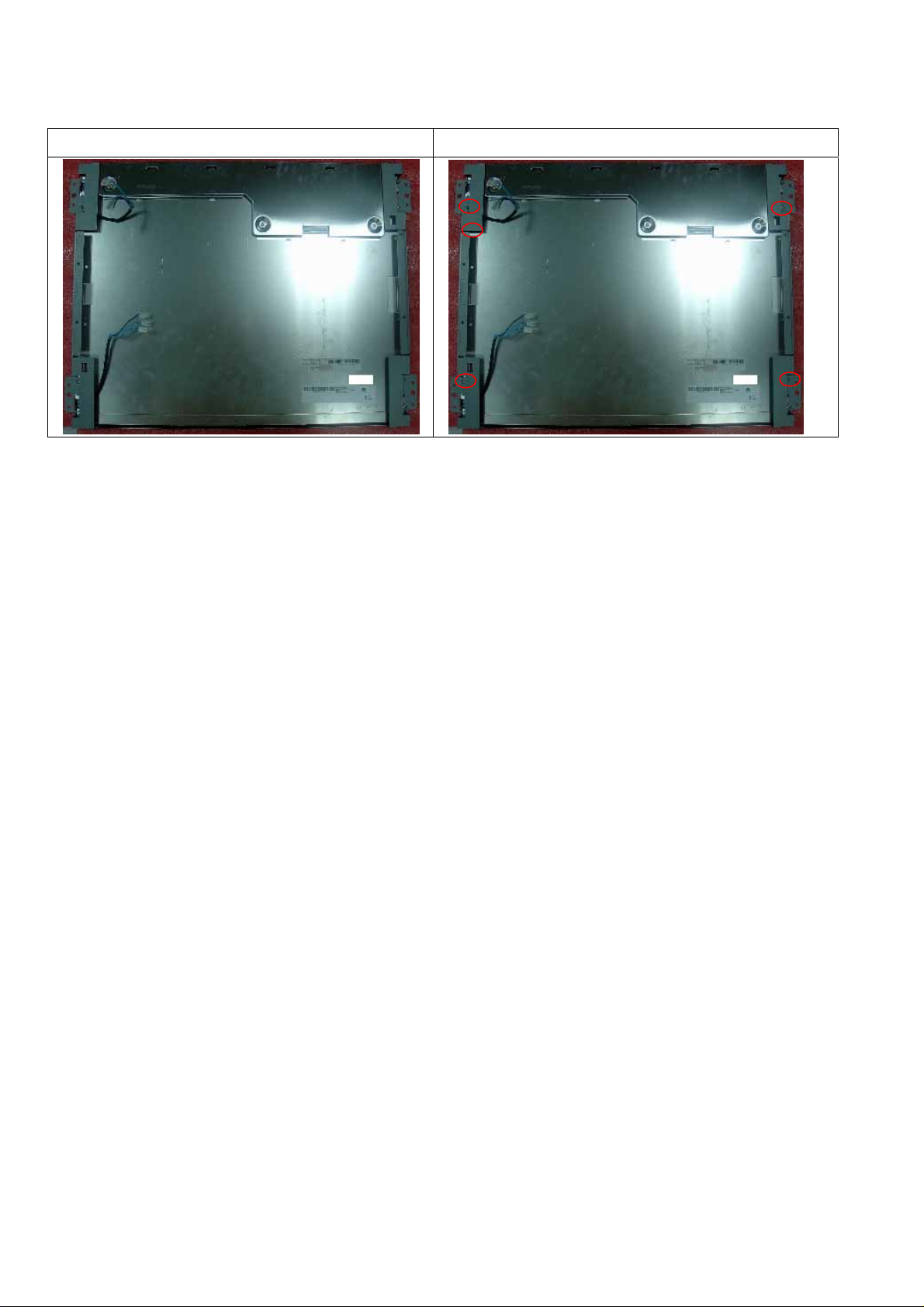
No.
1
Service Guide Version and Revision
Version
A00
Release Date
Jul-15 -2006
Revision
Original release
2
Page 3
Copyright
Copyright 2006 Acer Technology Corp.
All rights reserved.
This manual may not, in whole or in part, be copied, photocopied, reproduced, translated, or converted to any
electronic machine readable form without prior written permission of Acer Technology Corp.
ACER AT2002 Service Manual.
Printed in Fujian.
Disclaimer
The information in this guide is subj ec t to change without notice. Acer Incorp or a t ed mak es no rep resentations
or warranties, either expressed or implied, with respect to the contents hereof and specifically disclaims any
warranties of merchantability or fitness for any particular purpose. Any Acer Incorporated software described
in this manual is sold or licensed "as is". Should the programs prove defective following their purchase, the
buyer (and not Acer Incorporated, its distributor, or its dealer) assumes the entire cost of all necessary
servicing, repair, and any incidental or consequential damages resulting from any defect in the software.
Acer is a registered trademark of Acer Corporation.
Intel is a registered trademark of Intel Corporation.
Pentium and Pentium II/III are trademarks of Intel Corporation.
Other brand and product names are trademarks and/or registered trademarks of their respective holders.
Trademarks
All other trademarks are property of their respective owne rs.
Conventions
The following conventions are used in this manual:
Screen messages Denotes actual messages that appear on screen.
NOTE Gives bits and pieces of additional information related to the current topic.
WARNING Alerts you to any damage that might res ult from doing or not doing specific
actions.
CAUTION Gives precautionary measures to avoid possible hardware or software
problems.
IMPORTANT Remind you to do specific actions relevant to the accomplishment of
procedures.
Preface
Before using this information and the product it supports, please read the following general information.
1. This Service Guide provides you with all technical information relating to the BASIC CONFIGURATION
decided for Acer's "global" product offering. To better fit local market requirements and enhance product
competitiveness, your regional office may have decided to extend the functionality of a machine (e.g.
add-on card, modem, or extra memory capability). These LOCALIZED FEATURES will NOT be covered in
this generic service guide. In such cases, please contact your regional offices or the responsible
personnel/channel to provide you with furt he r tec hni ca l details.
3
Page 4

2. Please note WHEN ORDERING FRU PARTS, that you should check the most up-to-date info rmation
available on your regional web or channel. If, for whatever reason, a part number change is made, it will not
be noted in the printed Service Guide. For ACER-AUTHORIZED SERVICE PROVIDERS, your Acer office
may have a DIFFERENT part number code to those given in the FRU list of this printed Service Guide. You
MUST use the list provided by your regional Acer office to order FRU parts for repair and service of
customer machines.
Warning: (For FCC Certified Models)
Note: This equipment has been tested and found to comply with the limits for a Class B digital device,
pursuant to Part 15 of the FCC Rules. These limits ar e designed to provide reasonable protection against
harmful interference in a residential installation. This equipment generates, uses and can radiate radio
frequency energy, and if not installed and used in accordance with the instructions, may cause harmful
interference to radio communications. However, there is no guarantee that interference will no t occur in a
particular installation. If this equipment does cause harmful interference to radio or television reception, which
can be determined by turning the equipment off and on, the user is encouraged to try to correct the
interference by one or more of the following measures:
1. Reorient or relocate the receiving antenna.
2. Increase the separation between the equipment and receiver.
3. Connect the equipment into an outlet on a circuit different from that to which the receiver is connected.
4. Consult the dealer or an experienced radio/TV technician for help.
Notice:
1. The changes or modifications not expressly approved by the party responsible for compliance could void
the user's authority to operate the equipment.
2. Shielded interface cables and AC power cord, if any, must be used in order to comply with the emission
limits.
3. The manufacturer is not responsible for any radio or TV interference caused by unauthorized modification
to this equipment. It is the responsibility of the user to correct s uch interference.
As ENERGY STAR
®
Partner our company has determined that this product meets the ENERGY STAR
guidelines for energy efficiency.
®
Warning:
To prevent fire or shock hazard, do not expose the monitor to rain or moisture. Dangerous high voltages
are present inside the monitor. Do not open the cabinet. Refer servicing to qualified personnel only.
4
Page 5

Precautions
z Do not use the monitor near water, e.g. near a bathtub, washbowl, kitchen sink, laundry tub, swimming pool
or in a wet basement.
z Do not place the monitor on an unstable trolley, stand, or table. If the monitor falls, it can injure a person
and cause serious damage to the appliance. Use only a trolley or stand recommended by the manufacturer
or sold with the monitor. If you mount the monitor on a wall or shelf, uses a mounting kit approved by the
manufacturer and follow the kit instructions.
z Slots and openings in the back and bottom of the cabinet are provided for ventilation. To ensure reliable
operation of the monitor and to protect it from overheatin g, be sure these openings are not blocked or
covered. Do not place the monitor on a bed, sofa , rug, or similar surface. Do not place the monitor near or
over a radiator or heat register. Do not place the monitor in a bookcase or cabinet unless proper ventilation
is provided.
z The monitor should be operated only from the type of power source indicated on the label. If you are not
sure of the type of power supplied to your home, consult your dealer or local power company.
z The monitor is equipped with a three-pronged grounded plug, a plug with a third (grounding) pin. This plug
will fit only into a grounded power outlet as a safety feature. If your outlet does not accommodate the
three-wire plug, have an electrician install the correct outlet, or use an adapter to ground the appliance
safely. Do not defeat the safety purpose of the grounded plug.
z Unplug the unit during a lightning storm or when it will not be used for long periods of time. This will protect
the monitor from damage due to power surges.
z Do not overload power strips and extension cords. Overloading can result in fire or electric shock.
z Never push any object into the slot on the monitor cabinet. It could sh ort circuit parts causing a fire or
electric shock. Never spill liquids on the monitor.
z Do not attempt to service the monitor yourself; opening or removing covers can expose you to dangerous
voltages and other hazards. Please refer all servicing to qualified service personnel
z To ensure satisfactory operation, use the monitor only with UL listed computers which have appropriate
configured receptacles marked between 100 - 240V AC, Min. 5A.
z The wall socket shall be installed near the equipmen t and s hall be easily ac c es s ible.
Special Notes On LCD TV Monitors
The following symptoms are normal with LCD TV monitor and do not indicate a problem.
Notes
z Due to the nature of the fluorescent light, the screen may flicker during initial use. Turn off the Power Switch
and then turn it on again to make sure the flicker disappears.
z You may find slightly uneven brightness on the screen depending on the desktop pattern you use.
z The LCD TV screen has effective pixels of 99.99% or more. It may include blemishes of 0.01% or less such
as a missing pixel or a pixel lit all of the time.
z Due to the nature of the LCD TV screen, an afterimage of the previous screen may remain after switching
the image, when the same image is displayed for hour s. In this case, the screen is recovered slowly by
changing the image or turning off the Power Switch for hours.
5
Page 6
Table Of Contents
Monitor Features
General Specifications ……………………………………… 7
LCD TV Description ……………………………………… 8
Chapter 1
Chapter 2
Chapter 3
Chapter 4 Machine Disassembly
Precautions And Notices ……………………………………… 9
D-SUB PIN Distribution ……………………………………… 10
Factory Preset Display Modes ……………………………………… 11
LCD TV Panel Specification ……………………………………… 12
Panel Features ……………………………………… 12
General Specifications ……………………………………… 12
Mechanical Specifications ……………………………………… 12
Optical Specifications ……………………………………… 13
Connecting Peripherals
Front Panel Controls ……………………………………… 14
Remote Control & OSD Operating
Instructions
Using The Remote Control ……………………………………… 16
Using The OSD Menus 17
LOGO ……………………………………… 2
……………………………………… 7
……………………………………… 14
……………………………………… 1
……………………………………… 2
6
2
3
Chapter 5 Trouble Shooting
Chapter 6 White-Balance, Luminance Adjustment
FRU (Field Replaceable Unit) List
Chapter 7
Chapter 8 PCB Layout
Chapter 9 Schematic Diagram
Exploded Diagram ……………………………………… 38
EDID Data ………………………………………
………………………………………
……………………………………… 3
………………………………………
38
……………………………………… 4
………………………………………
29
4
37
0
70
6
Page 7
Model AT2002
Panel spec
Resolution (pixels) 800 x 600
Brightness (tpe.) 450 cd/m2
Contrast Ratio (tpe.) 600:1
Display colour 16.7 M
Viewing angle (tpe.) H: 160
o
; V:120
o
Response (tpe.) 16 ms (gray to gray)
Power supply
Input 100 V ~ 240 V - AC. (50/60 Hz)
Max. power consumption < 65 W
Power saving 5 W
Mechanical
Dimensions (W x H x D mm) 514 x 474 x 78
Weight (Kg) 7.4
Weight (lbs) 16.3
Gross weight (Kg) 9.4
Gross weight (lbs) 20.7
Wall Mounting 100mm x 100mm
Analog TV system
TV Colour system PAL, SECAM
Sound system B/G/D/K/I/L
Stereo system NICAM / A2
TV Tuner System PLL, 45.25 Mhz - 862.25 Mhz
Subtitles Teletext 1.5
Analog TV-tuner quantity 1
Terminal
Analog Tuner In Yes
SCART CVBS (In/Out), RGB (In), Audio R/L
AV CVBS, Audio R/L
S-Video S-Video, audio R/L share with AV
PC D-sub in Yes
PC audio-in Yes
Audio system
Speaker 5 W + 5 W
Monitor Features
Chapter 1
General Specifications
7
Page 8

LCD TV Description
The LCD TV will contain a main board (include audio), an I/O board, a switching power board, a function
keyboard (include an IR Board) and an Ear phone board. The main board and power board will house the flat
panel to control logic I2C bus, DDC, brightness control logic for LCD panel, DC-DC conversion to supply the
appropriate power to the whole board and transmitting TTL level signals into LCD Module to drive the LCD
display circuit.
The inverter board will drive the five CCFLs (Cold Cathode Fluorescent Lamp).
The switching power board will provides the power ON/OFF to control the TV and control LED indicator for
DPMS.
The function keyboard and Remote Control will provide the OSD control signal to the Main Board.
8
Page 9

Precautions And Notices
1-1 Assembly Precaution
(1) Please do not press or scratch LCD panel surface with anything hard. And do not so il LCD panel
surface by touching with bare hands (Polarize film, surface of LCD panel is easy to be flawed)
In the LCD panel, the gap between two glass plates is kept perfectly even to maintain display
characteristic and reliability . If this panel is subject to hard pressing, the following occurs :
(a) Uniform color (b) Orientation of liquid crystal becomes disorder
(2) Please wipe out LCD panel surface with absorbent cotton or soft cloth in case of it being soiled.
(3) Please wipe out drops of adhe siv e lik e saliv a and water in LCD panel surface immediately.
They might damage to cause panel surface variation and color change.
(4) Do not apply any strong mechanical shock to the LCD panel.
1-2 Operating Precaution
(1) Please be sure to unplug the power cord before remove the back-cover. (be sure the power is
turn-off)
(2) Please do not change variable resistance settings in MAIN-BOARD; they are adjusted to the most
suitable value. If they are changed, it might happen LUMINANCE does not satisfy the white
balance spec.
(3) Please consider that LCD backlight takes longer time to become stable of radiation characteristic in
low temperature than in room temperature.
(4) Please pay attention to displaying the same pattern for very long-time. Image might stick on LCD.
1-3 Storage Precaution
(1) When you store LCD for a long time, it is recommended to keep the temperature between -20°C -
60°C without the exposure of sunlight and to keep the humidity less than 85% RH.
(2) Please do not leave the LCD in the environment of high humidity and high temperature such a s
60°C, 95%RH.
(3) Please do not operate the LCD in the environment of abnormal temperature, below 0°C.
1- 4 High Voltage Warning
The high voltage was only generated by Power support part, if carelessly contacted the transformer
on this module, can cause a serious shock.
9
Page 10
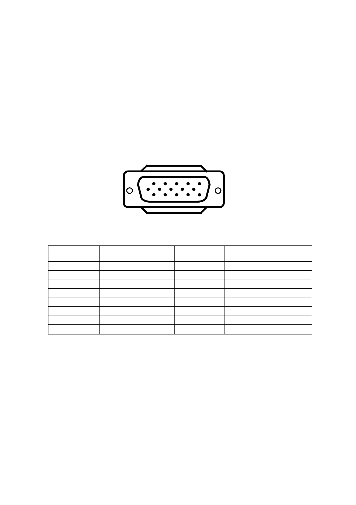
D-SUB PIN Distribution
This procedure gives you instructions for installing and using the LCD TV display.
(1) Position the display on the desired operation and plug the power cord into a convenient AC outlet.
Three-wire power cord must be shielded and is provided as a safety precaution as it connects the chassis
and cabinet to the electrical conduct ground. If the AC outlet in your location does not have provisions for
the grounded type plug, the installer should attach the proper adapter to ensure a safe ground potential.
(2) Connect the 15-pin color display shielded signal cable to your signal system device and lock both screws
on the connector to ensure firm grounding. The connector information is as follow:
1
6
11 15
15 - Pin Color Display Signal Cable
5
10
Pin NO. Description Pin NO. Description
1 Red Video 9 +5V(PC97)
2 Green Video 10 VGA-CONN(Sync GND)
3 Blue Video 11 Ground
4 Ground 12 SDA(DDC Data)
5 Ground 13 H-Sync.
6 Red Ground 14 V-Sync.
7 Green Ground 15 Serial Clock for DDC
8 Blue Ground
10
Page 11
Factory Preset Display Modes:
Analog RGB Signal Timing
Vertical Horizontal Sync Polarity Presence Screen Mode
Dots × Lines
720 ×400 70.1 31.5 NEG POS YES YES YES
640 ×480
800 ×600
Frequency Frequency FULL
Horizontal Vertical Horizontal Vertical
(Hz) (KHz)
59.9 31.5 NEG NEG YES YES YES
72.8 37.9 NEG NEG YES YES YES
75.0 37.5 NEG NEG YES YES YES
60.3 37.9 POS POS YES YES YES
72.2 48.1 POS POS YES YES YES
75.0 46.9 POS POS YES YES YES
(16:9)
11
Page 12

LCD TV Panel Specification
Panel Features
-High brightness (450 nits)
- High contrast ratio (
- Fast response time (
- High color saturation NTSC
- WX
GA (800 x 600 pixels) resolution
- DE (Data Enable) only mode
- LVDS (Low Voltage Differential Signaling) interface
- Optimized response time for 50/60 Hz frame rate
- Ultra wide viewing angle:
- 180 degree rotation display option
General Specifications
NO. Item Specification Remark
1 Display resolution(pixel)
700:1)
16ms)
72%
160(H)/140(V) (CR>20) Super MVA technology
800x3(H)×600(V)
2 Display Mode TN Type, Normally White + SWV Film
3 Active area (mm)
4 Screen size (inch) 20.1(Diagonal)
5 Pixel pitch (mm)
6 Color configuration R. G. B. Vertical stripe
7 Display Color 16.2M (6 bit + FRC)
8 Typical white Luminance 450 nit (typ.)
9 Contrast ratio 700:1
10 Color Gamut 72% typ. of NTSC coverage
11 Response Time 16ms typ. (Tr+Tf)
12 Electrical Interface TTL 1 port
13 Overall dimension (mm)
14 Weight (g) 3500
15 Surface Treatment Anti-Glare type
16 RoHS RoHS compliance
408(H)×306(V)
0.51(H)×0.51(V)
448(W)×347(H)×23(D)(max.)
12
Page 13
Optical Specifications
-
Test Conditions
Item Symbol Min.
Power
supply
voltage
Input voltage VCC 4.75 5.0 5.25 V
Current
consumption
I
A
Typ.
- 0.8 1.0 Arms
Max. Unit Remark
Inrush current I
Power ripple
voltage
Internal
logic
Low voltage
High voltage
Optical Specifications
Item Symbol Condition
Response time
Rising time
Falling time
Contrast ratio(center of screen)
Viewing angle
Top
Bottom
Left
Right
RUSH
VRP - - 100 mVp-p
VIL 0 - 1.0 V
VIH 2.3 - 3.3 V
Tr
Tf
CR
- - 3.0 Apeak
θ=0°
θ=0°
CR≧10
Specification
Min. Typ. Max.
-
-
600 700
65
55
65
65
11
5
80
60
80
80
15
10
-
-
-
-
Unit Remark
Deg.
ms
Brightness (center of screen)
Y
L
Wx
Color chromaticity (CIE)
Wy
Rx
Ry
Color Saturation (NTSC) 72 %
White uniformity
Gx
Gy
Bx
By
δ
W
θ=0°
θ=0°
70 - - %
350 450 - nit
0.249 0.279 0.309
0.260 0.290 0.320
0.607 0.637 0.667
0.311 0.341 0.371
0.268 0.298 0.328
0.568 0.598 0.628
0.113 0.143 0.173
0.028 0.058 0.088
13
Page 14
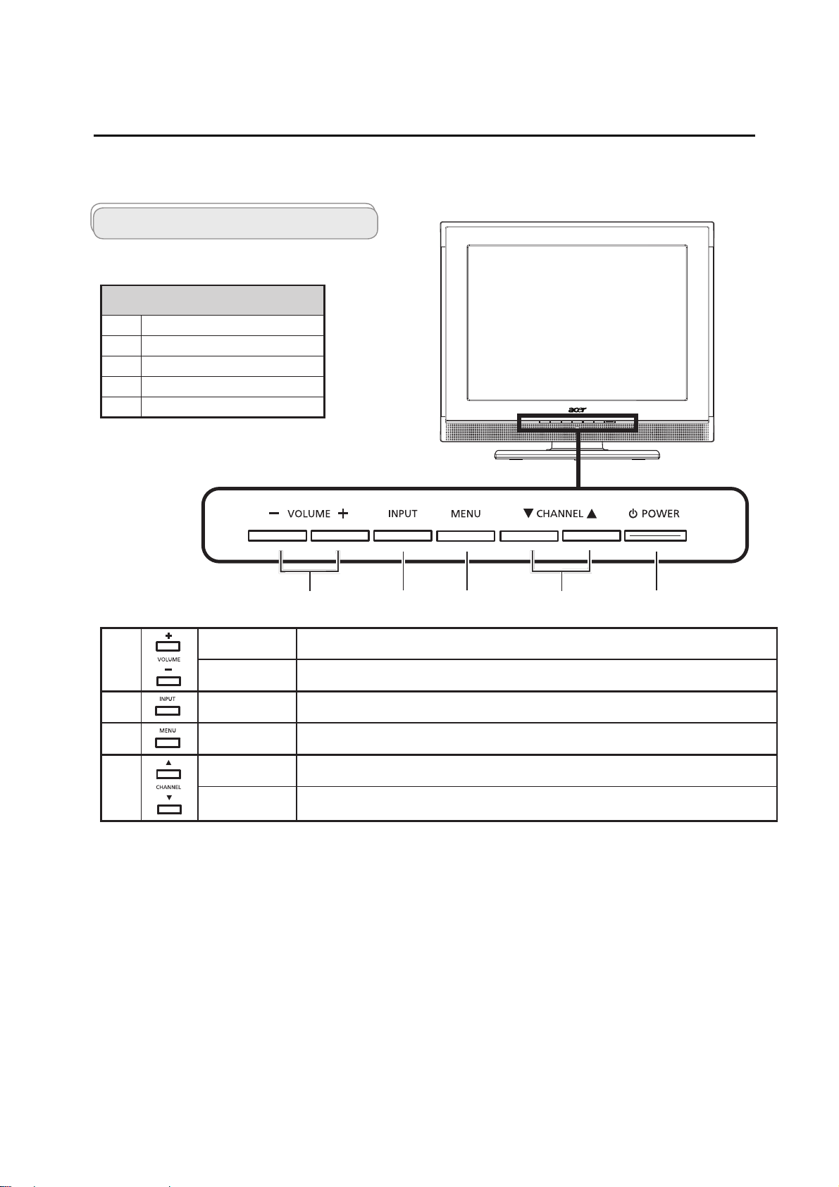
Front panel view
1 Volume +/-
2 Input key
3 Menu key
4 Channel up/down
5 Power On/Off
Your LCD TV overview
1
Volume up When the OSD is on, functions the same as the Right arrow
Volume down When the OSD is on, functions the same as the Left arrow
2
Input key When the OSD is on, press this button to confirm selection
3
Menu key Turns the OSD menu ON and OFF
4
Channel up When the OSD is on, functions the same as the Up arrow
Channel
down
When the OSD is on, functions the same as the Down arrow
1 2 3 4
5
Connecting Peripherals
Chapter 2
Front panel controls
14
Page 15
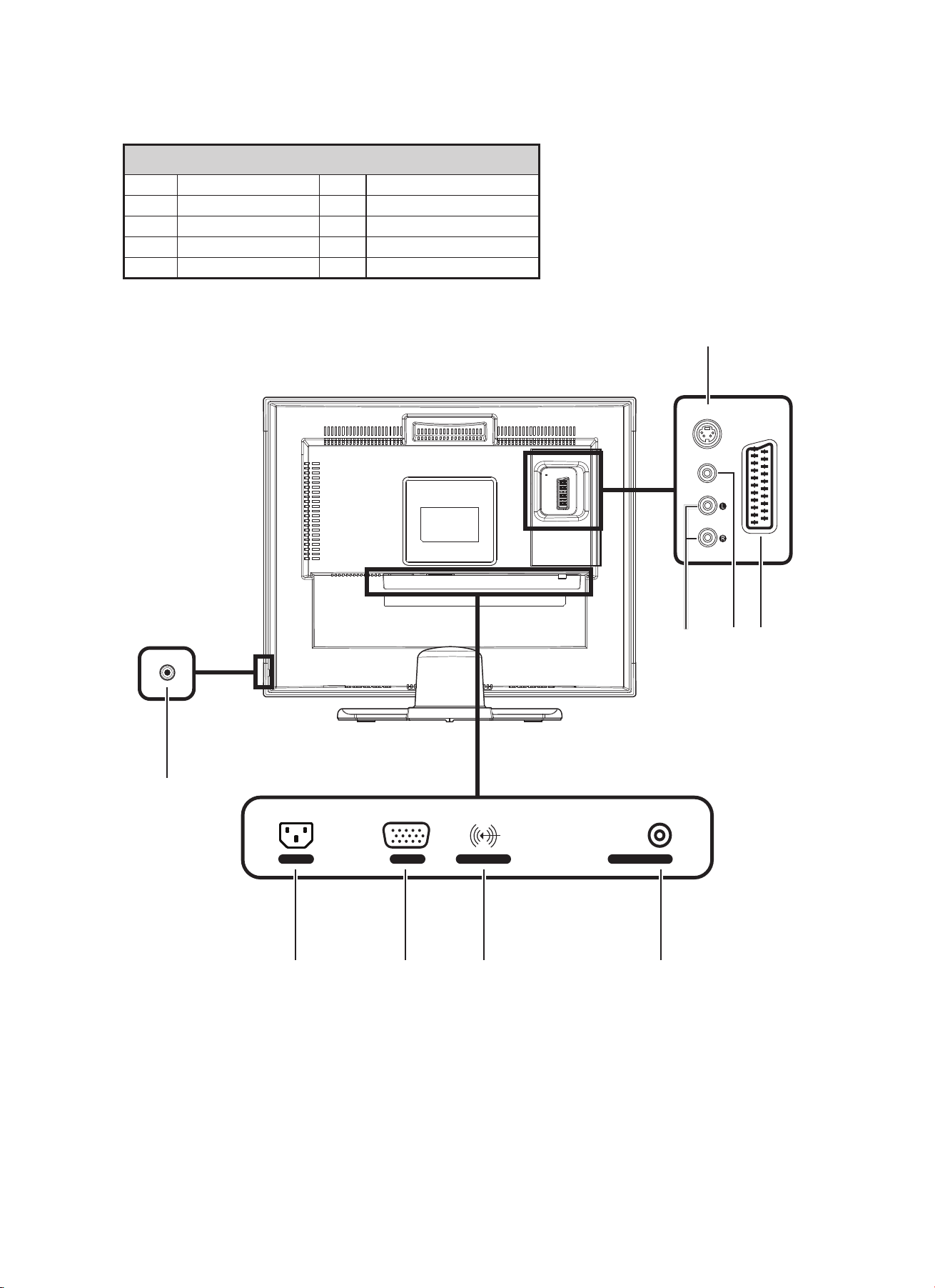
Rear panel view
1 S-Video 2 SCART
3 CVBS 4 AV-Audio L/R
5 Analog antenna 6 PC Audio-in
7 VGA-in 8 AC-in
9
Earphone
AC-IN
VGA PC AUDIO-IN ANALOG TUNER
AUDIO
VIDEO
S-VIDEO
SCART
9
8
7 6 5
4
3 2
1
Page 16
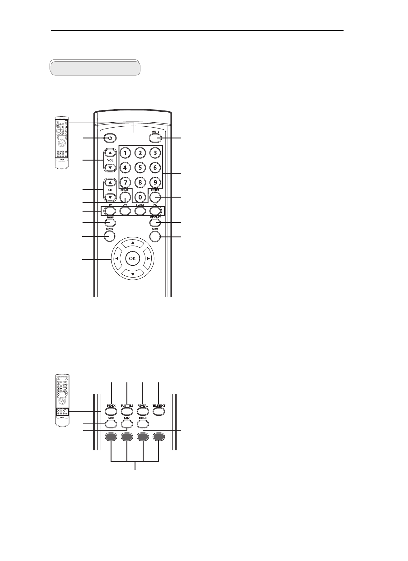
Remote Control & OSD Operating instructions
Chapter 3
Using the Remote Control
Remote control
General keys
1
3
4
6
8
9
11
13
2
5
7
10
12
1 POWER
Press to turn your TV on/off.
2 MUTE
3 VOL (up/down)
4 CH (up/down)
5 Number keys
6 RECALL
7 ENTER
8 Input buttons (TV/AV/SCART/PC)
9 SLEEP
10 DISPLAY
11 MENU
12 MPX
13 Directional keys/OK
Press to toggle audio on and off.
Press to increase or decrease the volume.
Press to sequentially select the TV channel.
.
Press to return to the previous channel.
Press to confirm channel number selection.
Press to select correct input mode.
Press to set a time period after which the TV will switch
itself to standby (15, 30, 45, 60, 90 or 120 minutes).
Press to display input/channel information
(dependent on input/source type).
Press to open or close the Menu.
Press to select the sound input, displayed in the top righthand corner (mono, stereo, bilingual).
VOL (up/down), CH (up/down)
Teletext
182 3 4
5
6
7
1 INDEX
Press to go to the index page
2 SUBTITLE
Press to view subtitles on the screen.
3 REVEAL
Press to reveal hidden telext information
4 TELETEXT
Press to switch from TV/AV to Teletext mode.
5 SIZE
Press once to zoom teletext page to 2X.
Press again to resume.
6 MIX
Press to overlay teletext page on the TV image.
7 HOLD
Press to pause the current teletext page in multi-page
viewing mode.
8 Colour buttons (R/G/Y/B)
Operates corresponding button on the teletext page.
16
Page 17
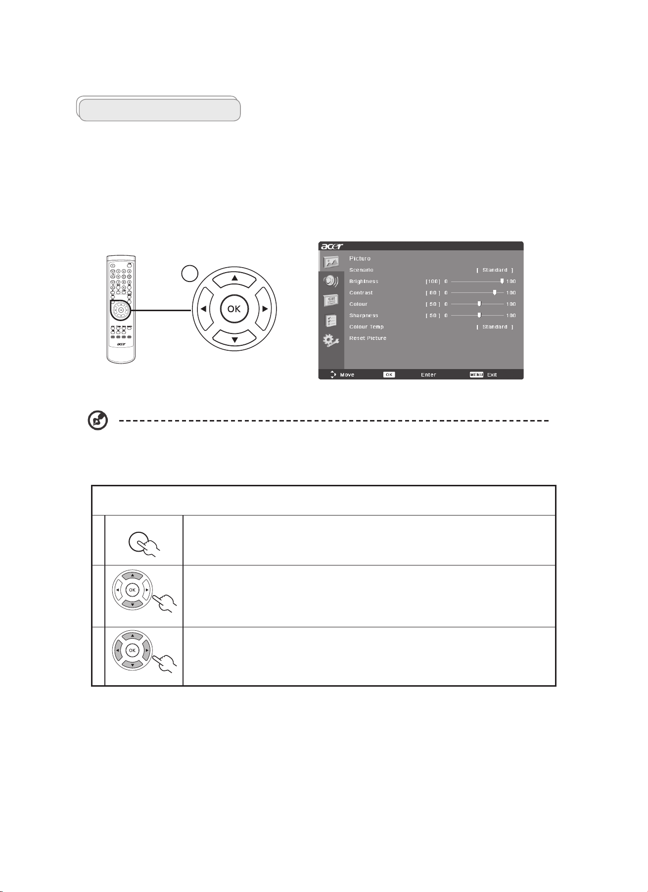
OSD navigation
Many of the advanced settings and adjustments are available through using the OSD (onscreen display) menus, as shown in the
example screenshot below.
Basic operations required to navigate these menus (Picture, Audio, Channel management, Options, Settings) are described in this
section.
There are five main OSD menus. These are: Picture, Audio, Channel management, Options and Settings.
Use the following method to navigate these menus.
1
MENU
Press the MENU button on the remote control or the MENU button on the control panel.
2
Select your desired menu by using the up and down directional keys to switch between the five
menus.
3
Use the directional keys to interact with the menu. The up / down directions will scroll through the
menu options, while left/right will adjust the different settings (for example, in the Picture menu,
settings such as brightness, contrast, etc.). Press MENU to exit.
You can also interact with these menus using the front panel controls. Please see "Front panel view" on page 4 for
details.
Navigating the OSD with the remote control
MENU
Using The OSD Menus
17
Page 18
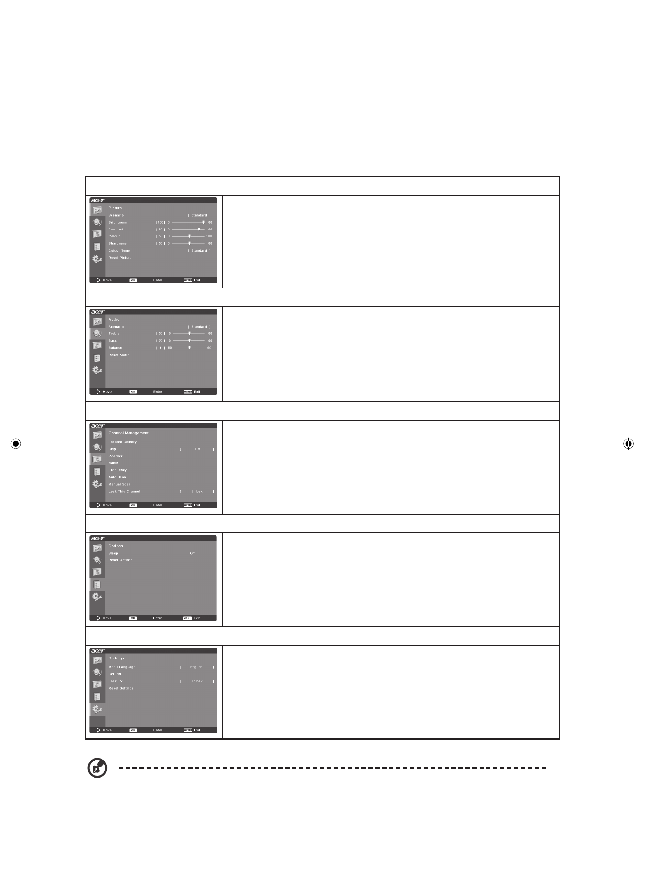
Adjusting the OSD settings
The OSD can be used for adjusting the settings of your LCD TV.
Press the MENU key to open the OSD. You can use the OSD to adjust the picture quality, audio settings, channel settings and
general settings. For advanced settings, please refer to following page:
Adjusting the picture quality
1 Press the MENU key to bring up the OSD.
2 Using the directional keys, select
Picture from the OSD. Then navigate to the picture
element you wish to adjust.
3 Use the left or right keys to adjust the sliding scales.
4 The
Picture menu can be used to adjust the current Scenario mode, brightness,
contrast, colour, sharpness and other image-related qualities.
Adjusting the audio settings
1 Press the MENU key to bring up the OSD.
2 Using the directional keys, select
Audio from the onscreen display. Then navigate to
the feature you wish to adjust.
3 Use the left or right keys to adjust the sliding scale. Press
OK to save.
4 The
Audio menu can also be used to adjust the treble, balance, sound effects and
other important sound-related settings
Adjusting the channel management
1 Press the MENU key to bring up the OSD.
2 Using the directional keys, select
Channel management from the OSD.
3 Use the directional keys to navigate the menus.
4 The
Channel management menu can be used to adjust frequency, and set the channel
namings.
Adjusting other options
1 Press the MENU key to bring up the OSD.
2 Using the directional keys, select
Options from the OSD.
3 Use the directional keys to navigate the menus.
4 The
Options menu can be used to select the picture aspect-ratio mode and reset
options.
Adjusting the settings
1 Press the MENU key to bring up the OSD.
2 Using the directional keys, select
Settings from the OSD. Then navigate to the feature
you wish to adjust.
3 The
Settings menu can be used to adjust the menu language, set the sleep timer and
other important settings.
The options available on the OSD may vary depending on the TV signal source.
Page 19
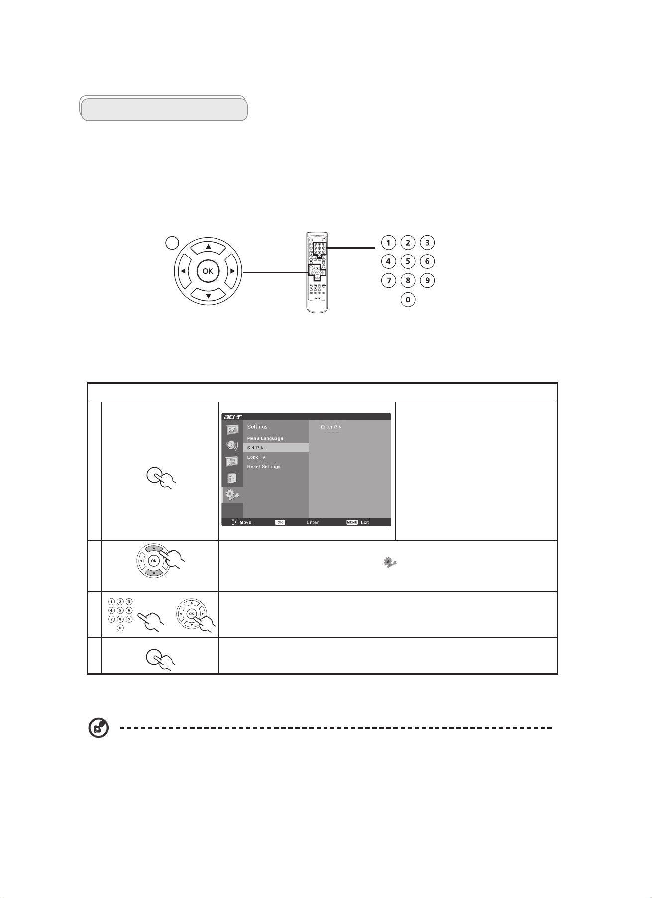
Advanced features
Lock TV
Locking TV content
Lock TV is a handy feature that can block a single channel, multiple channels or all TV sources.
Lock TV allows you to enter a password and effectively stop anyone without the password from watching TV.
Setting a personal PIN
1
MENU
Press the MENU key on the remote
control to bring up the OSD.
2
Use the directional keys to navigate to the Settings menu. Then select Set PIN.
(see note)
3
MENU
Enter a four-digit password. Type it again and press OK to reconfirm.
4
MENU
Press MENU to exit.
To enable this feature:
The default PIN for this TV is "0000." First enter "0000" when you want to change the PIN. If you forget your PIN,
please enter 6163 to reset.
MENU
Page 20
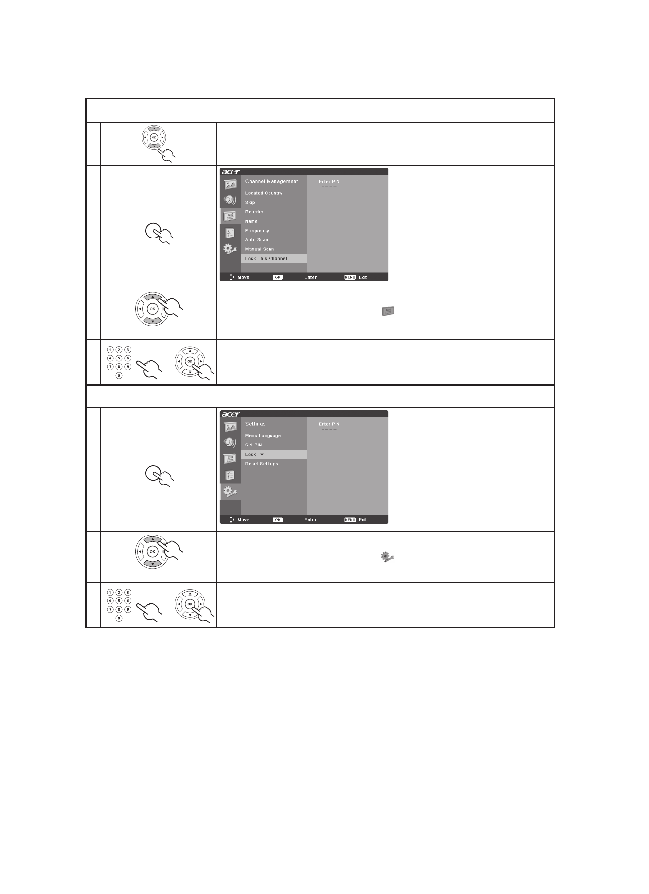
Locking a single channel
1 Navigate to the channel you wish to manage.
2
MENU
Press the MENU key on the remote
control to bring up the OSD.
3
Use the directional keys to navigate to the Channel management menu. Then select
Lock This Channel.
4
MENU
Enter your PIN. Type it again and press OK to reconfirm.(see page 12)
Locking your TV
1
MENU
Press the MENU key on the remote
control to bring up the OSD.
2
Use the directional keys to navigate to the Settings menu. Then select Lock TV.
3
MENU
Enter your PIN. Type it again and press OK to reconfirm. (see page 12 note)
Page 21
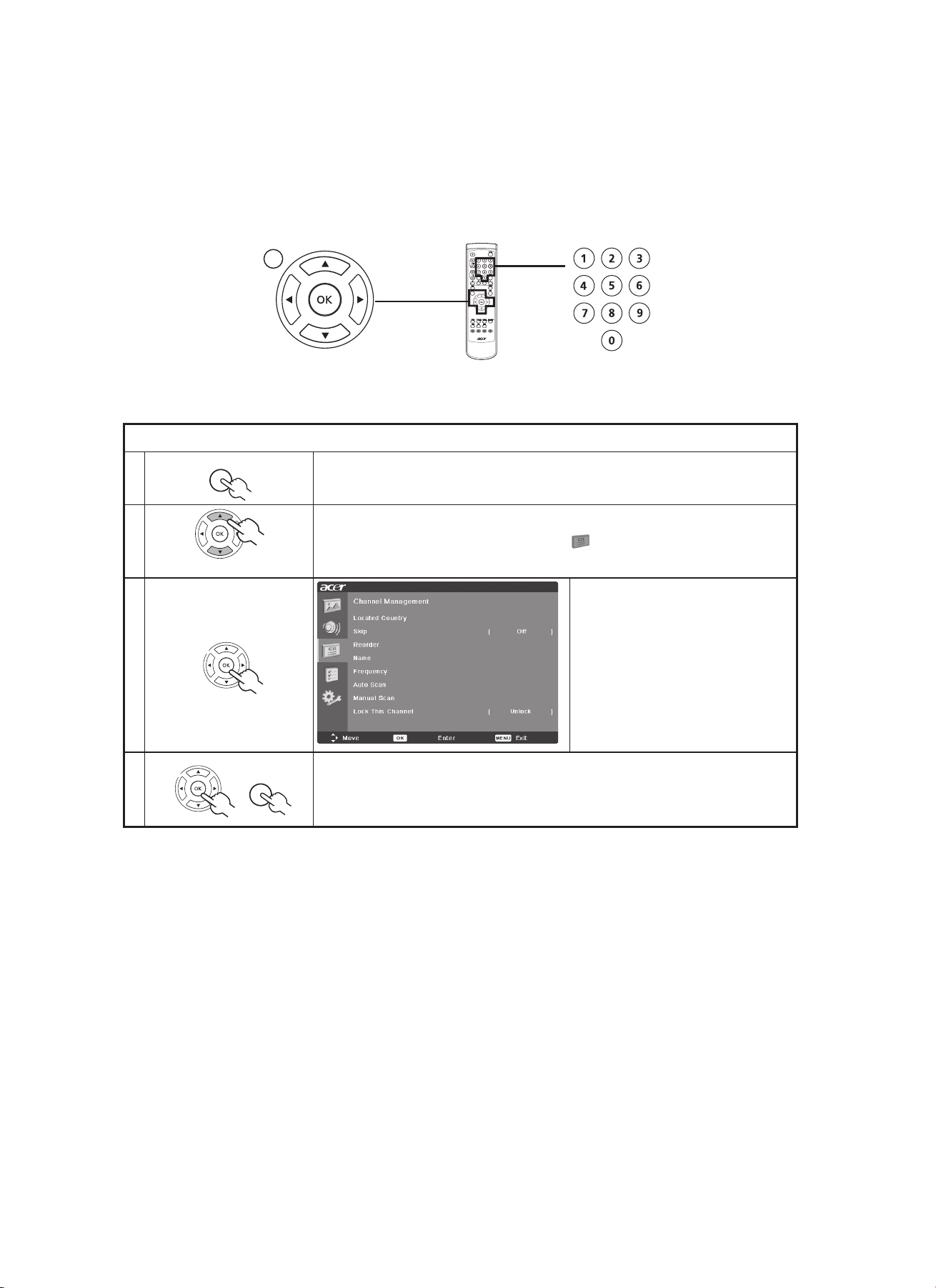
Scanning for channels
1
MENU
Press the MENU key on the remote control to bring up the OSD.
2
Use the directional keys to navigate and select Channel Management.
3
MENU
Highlight Auto Scan. Then, select Start
and press OK to begin.
4
MENU
MENU
Select OK and press MENU to exit.
Re-scan for channels
The first time you completed the setup wizard, all available channels were listed. If you need to re-scan for new channels, please
follow the steps below:
MENU
Page 22

Logo
When the monitor is power on, the LOGO will be showed in the center, and disappear slowly.
How To Optimize The DOS-Mode
Plug And Play
Plug & Play DDC2B Feature
This monitor is equipped with VESA DDC2B capabilities according to the VESA DDC STANDARD. It allows
the monitor to inform the host system of its identity and, depending on the level of DDC used, communicate
additional information about its display capabilities.
The DDC2B is a bi-directional data channel based on the I²C protocol. The host can request EDID
information over the DDC2B channel.
This monitor will appear to be non-functional if there is no video input signal. In order for this
monitor to operate properly, there must be a video input signal.
This monitor meets the Green monitor standards as set by the Video Electronics Standards Association
(VESA) and/or the United States Environmental Protection Agency (EPA) and The Swedish Confederation
Employees (NUTEK). This feature is designed to conserve electrical energy by reducing power
consumption when there is no video-input signal present. When there is no video input signals this monitor,
following a time-out period, will automatically switch to an OFF mode. This reduces the monitor's internal
power supply consumption. After the video input signal is restored, full power is restored and the display is
automatically redrawn. The appearance is similar to a "Screen Saver" feature except the display is
completely off. The display is restored by pressing a key on the keyboard, or clicking the mouse.
Using The Right Power Cord
The accessory power cord for the Northern American region is the wallet plug with NEMA 5-15 style and is
UL listed and CSA labeled. The voltage rating for the power cord shall be 125 volts AC.
Supplied with units intended for connection to power outlet of personal computer: Please use a cord set
consisting of a minimum No. 18 AWG, type SJT or SVT three conductors flexible cord. One end terminates
with a grounding type attachment plug, rated 10A, 250V, CEE-22 male configuration. The other end
terminates with a molded-on type connector body, rated 10A, 250V, having standard CEE-22 female
configuration.
Please note that power supply cord needs to use VDE 0602, 0625, 0821 approval power cord in European
counties.
2
2
Page 23
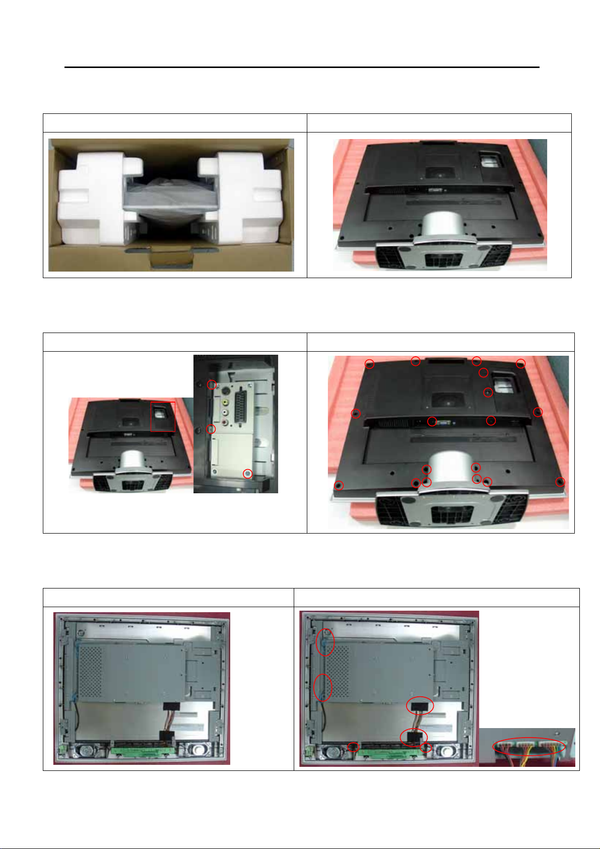
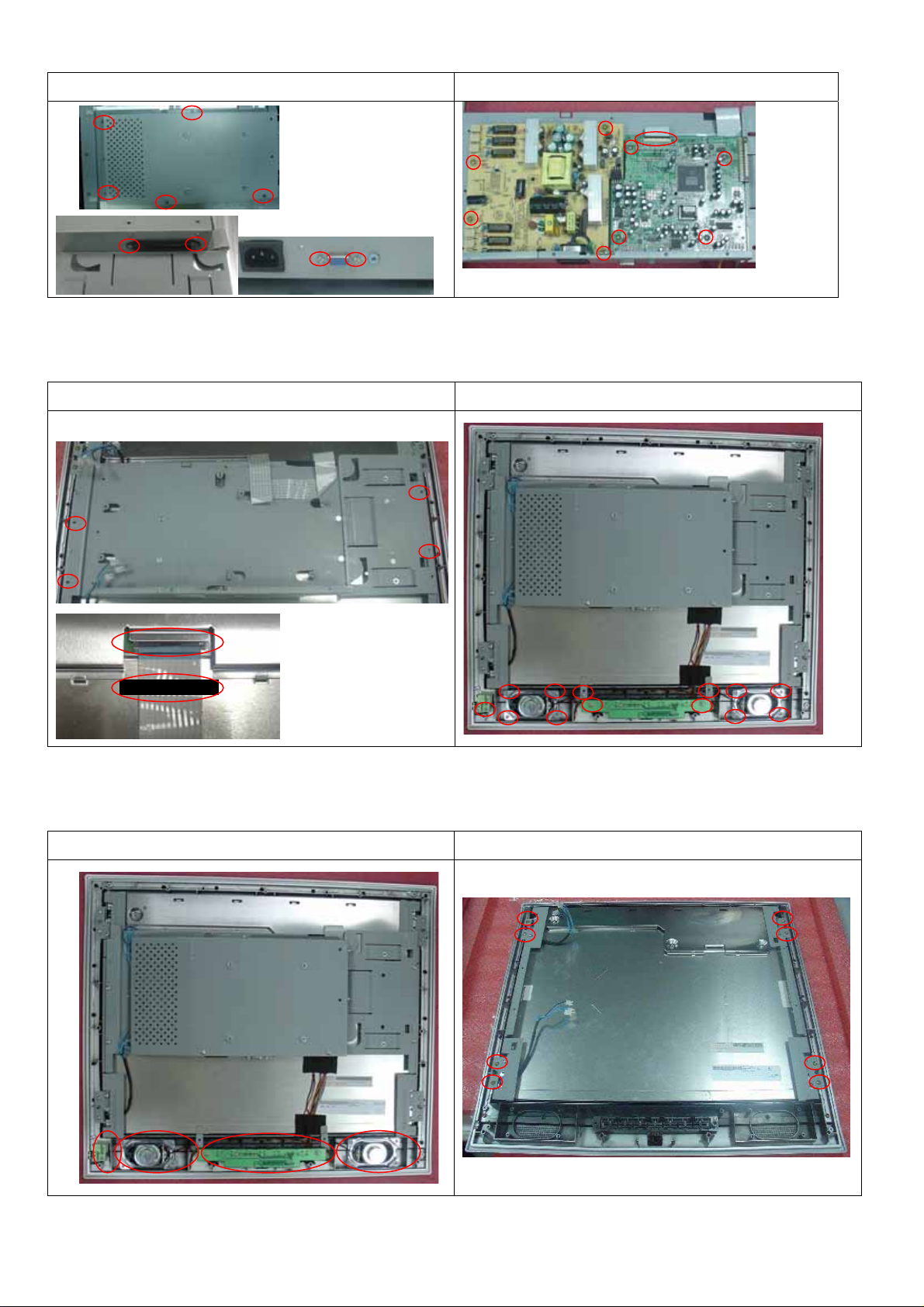
Machine Disassembly
Chapter 4
LCD TV AT2002 series de-assembling procedure
1. Move the monitor our from carton 2. Put the monitor on desk & face down
3. Remove the midea cover & SCREW &TV BOX 4. Loose the screws & remove the stand
5. Remove the bezel & cover 6. TAKE OFF THE CABLE & TAPE
23
Page 24
7. Loose the shielding screw & shielding 8. Loose the PCB’A screw & LVDS cable
9. Loose the shielding & tape & LVDS cable
11. Remove the Button/B&
earphone/b & speaker
10.Loose the Button/B&
12. Loose the bezel screw
earphone/b & speaker screw
Page 25
13. Remove the bezel 14. Remove the bkt l/r screw & bkt l/r
Page 26
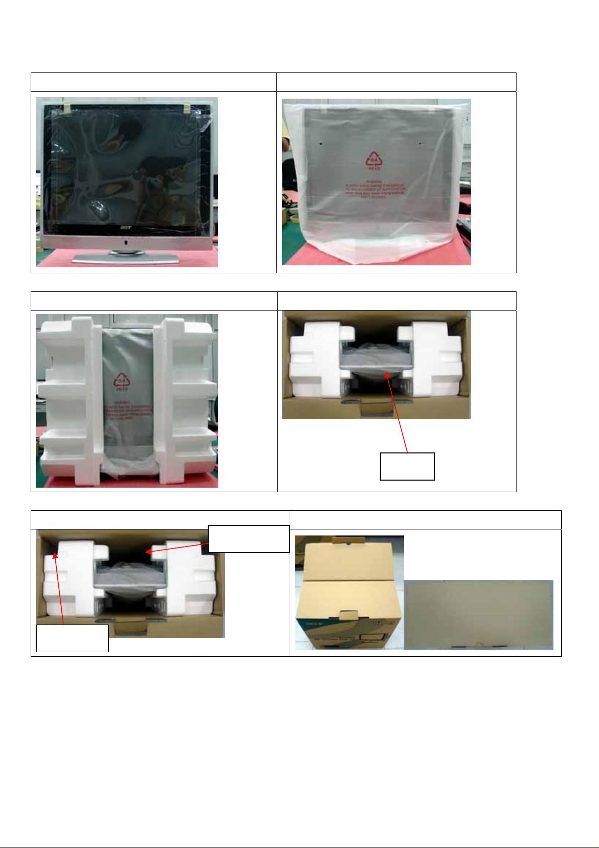
LCD TV AT2002 series packing method
1. Sticker on LCD protection film 2. Put the monitor into the PE or EPE bags
3. Put on the end-cap left / right 4. Put the monitor into carton
Face-up
5. Put all accessories into carton 6. Seal the monitor
Users manual
Power cable
Page 27

LCD TV AT2002 series handling Notice
Correct Method Incorrect method
Correct Method Incorrect method
Correct Method Incorrect method
Page 28

Correct Method Incorrect method
Correct Method Incorrect method
Page 29

Trouble Shooting
No
1. No Power
NO POWER
Check Power-board
CN201 pin1 12V, pin5 5V
Correct ??
Yes
Check FB14 3.3V
FB27 1.8V correct?
Change
M/B
No
Separate MB &
power-board
Check CN201 pin1
12V, pin5 5V
Correct ??
Separate MB &
I/O-board
Check CN201 pin1
12V, pin5 5V
Correct ??
Chapter 5
Change
Power-board
Yes
Yes
Change
I/O-board
Change
M/B
No
Page 30

p
2. No picture, No backlight.
No picture
No backlight
Check Power/B CN201
Pin8 3.3V correct?
No
Yes
Change
power board
Change
power board
No
Check LCD panel
Page 31

3. No Characters , Missing Color
No Characters , Missing Color
Check CN6
Pin6~9 5V correct?
YES
Check
TTL FFC cable
No
Check LCD panel
Yes
No
Change
M/B
Change
TTL FFC cable
Page 32

4. VGA mode Always show NO SIGNE
VGA always show No
Signal
Check VGA cable
correct?
No
Change
VGA cable
YES
Yes
Check input CN2
Pin13 H-sync ,pin14 V-sync
correct?
No
Check PC
Change
M/B
Page 33

always show
5. Video mode always show NO SIGNEL
Video-mode always show
No SignalVideo-mode
Check Video cable
correct?
YES
Check I/O board
correct?
No
Change I/O
board
No
Yes
Change
Video cable
Change
M/B
Page 34

White-Balance, Luminance Adjustment
Chapter 6
Approximately 30 minutes should be allowed for warm up before proceeding white
balance adjustment.
Before started adjust white balance ,please setting the Chroma-7120
MEM. channel 2 to 10000
( our 12000 parameter is x = 272 ± 15, y = 278 ± 15, Y = 350 ± 7 cd/m2 ;
10000 parameter is x = 279 ± 15, y = 290 ± 15, Y = 350± 7 cd/m
8000 parameter is x = 295 ± 15, y = 305 ± 15, Y = 350± 7 cd/m
MEM. channel 3 to 8000
color,
color,
2
MEM.
2
;
MEM. Channel 1 to 12000
color,
Color Temp. 12000 10000 8000
X 272 279 295
Y 278 290 305
Y 350 350 350
How to setting MEM. channel you can reference to Chroma-7120 user guide or simple use “ SC” key and
NEXT
“
Following is the procedure to do white-balance adjust
” key to modify x, y , Y value and use “ID” key to modify the TEXT description
I.Press Number key Power key + manual will into the factory mode, and press Menu key the
OSD will show menu and a word “F” at LEFT top of Menu.
1. In the factory mode select “COLOR TEMP” may be select the difference color temp.
2. Select SCALER Adjustment:
RG, GG, BG Æ R, G, B Gain adjust.
RB, GB, BB Æ R, G, B Bias adjust.
<Notes: the R, G, B gain use 9 bits, and R, G, B bias use 10 bits to save the value in EEPROM,
so if the R, G, B gain and bias is 255 to 256, the “P0 256”will change to “P10”>
Notes: adjust AV mode the same as PC mode, except the luminance (Pc mode is 350cd/m2,
Av is 350cd/m2).
II. Bias (Low luminance) adjustment:
1. Set the raster pattern (Black pattern with 800×600) Input.
2. Set the contrast on OSD window to the value=80, Brightness set to “80”
3. Adjust the brightness on OSD until chroma 7120 measurement reach the lowest value.
34
Page 35

III, Gain adjustment:
A. Adjust 12000 color-temperature:
1. Set the Contrast of OSD function to 80 and Adjust Brightness to chroma-7120 Y>350 cd/m2
2. Switch the chroma-7120 to RGB-mode (with press “MODE” button)
3. Switch the MEM.channel to Channel 02 (with up or down arrow on chroma-7120)
4. The LCD-indicator on chroma-7120 will show x = 272 ± 15, y = 278 ± 15, Y = 350 ± 7 cd/m2
5. Adjust the Color (user) Mode: RED on OSD window, until chroma 7120 indicator reached the value R=100
6. Adjust the Color (user) Mode: GREEN on OSD window, until chroma-7120 indicator reached the value G=100
7. Adjust the Color (user) Mode: BLUE on OSD window, until chroma-7120 indicator reached the value B=100
8. Repeat above procedure (Item 5,6,7) until chroma-7120 RGB value meet the tolerance =100±2
9. Switch the chroma-7120 to x, y, Y mode With press “MODE” button to check the color temp is in SPEC. or not.
10. Press MENU to exit the SCALER page and press Save to save the current color temp.
B. Adjust 10000 color-temperature:
1. Set the Contrast of OSD function to 80 and Adjust Brightness to chroma-7120 Y>350 cd/m2
2. Switch the chroma-7120 to RGB-mode (with press “MODE” button )
3. Switch the MEM.channel to Channel 02 ( with up or down arrow on chroma-7120 )
4. The LCD-indicator on chroma-7120 will show x = 279 ± 15, y = 290 ± 15, Y = 35
5. Adjust the Color(user)Mode: RED on OSD window, until chroma 7120 indicator reached the value R=100
6. Adjust the Color (user) Mode: GREEN on OSD window, until chroma-7120 indicator reached the value G=100
7. Adjust the Color(user)Mode: BLUE on OSD window, until chroma-7120 indicator reached the value B=100
8. Repeat above procedure (item 5,6,7) until chroma-7120 RGB value meet the tolerance =100 ±2
9. Switch the chroma-7120 to x, y, Y mode with press “MODE” button
10. Press MENU to exit the SCALER page and press Save to save the current color temp.
0 ± 7 cd/m2
C. Adjust 8000 color-temperature:
1. Set the Contrast of OSD function to 80 and Adjust Brightness to chroma-7120 Y>350 cd/m2
2. Switch the chroma-7120 to RGB-mode (with press “MODE” button)
3. Switch the MEM.channel to Channel 03 (with up or down arrow on chroma-7120)
4. The LCD-indicator on chroma-7120 will show x = 295 ± 15, y = 305 ± 15, Y = 350 ± 7 cd/m2
5. Adjust the Color (user) Mode: RED on OSD window, until chroma 7120 indicator reached the value R=100
6. Adjust the Color (user) Mode: GREEN on OSD window, until chroma-7120 indicator reached the value
G=100
7. Adjust the Color (user) Mode: BLUE on OSD window, until chroma-7120 indicator reached the value
B=100
8. Repeat above procedure ( item 5,6,7) until chroma-7120 RGB value meet the tolerance =100 ± 2
9. Switch the chroma-7120 to XyY mode With press “MODE” button
10. Press MENU to exit the SCALER page and press Save to save the current color temp.
3
5
Page 36

FRU (Field Replaceable Unit) List
This chapter gives you the FRU (Field Replaceable Unit) listing in global configurations of AT2002.Refer to
this chapter whenever ordering for parts to repair or for RMA (Return Merchandise Authorization).
NOTE:
information available on your regional web or channel (http://aicsl.acer.com.tw/spl/). For whatever reasons
a part number change is made, it will not be noted in the printed Service Guide. For ACER AUTHORIZED
SERVICE PROVIDERS, your Acer office may have a DIFFERENT part number code from those given in
the FRU list of this printed Service Guide. You MUST use the local FRU list provided by your regional Acer
office to order FRU parts for repair and service of customer machines.
NOTE:
regulations on how to dispose it properly, or follow the rules set by your regional Acer office on how to
return it.
Please note WHEN ORDERING FRU PARTS, that you should check the most up-to-date
To scrap or to return the defective parts, you should follow the local government ordinance or
Chapter 7
36
Page 37

Exploded Diagram (Model: AT2002)
Page 38

Y
Parts
BOARD
CATEGORY PARTNAME DESCRIPTION
MAIN BOARD FIRMWARE CTRL
POWER BOARD POWER BOARD
CASE / COVER ASSEMBL
BUTTON BOARD KEY CTRL FIRMWARE
EARPHONE BOARD
LCD PANEL 20.1"
A201SN02 V5
EARPHONE CTRL
FIRMWARE
20.1" A201SN02 V5
FRONT BEZEL
39 Chapter 4
FRONT BEZEL
WITH BEZEL PLATE
Page 39

CATEGORY PARTNAME DESCRIPTION
BACK COVER BACK COVER
BASE
BASE TO SUPPORT
THE STAND
40 Chapter 4
Page 40

PCB Layout
.
Chapter 7
40
Page 41

Page 42

Page 43

Page 44

Page 45

Page 46

Page 47

Page 48

CAM350 V 7.6 : Fri Jun 02 14:18:32 2006 - (Untitled) : silk_top.art
Page 49

Page 50

Page 51

Page 52

Page 53

Page 54

Page 55

Page 56

Page 57

Page 58

Page 59

Page 60

Page 61

Page 62

Page 63

Page 64

Page 65

Page 66

Page 67

Page 68

Page 69

Page 70

5
4
3
2
1
+5V_IN
D D
5V_SCL6
TUNER_MONO6
SCART-1-OUT_L6
C C
SCART-1-IN_PIN8
B B
+12V_SW
R6
3K/6F
R8
1K/6F
GND
SCART-1-IN_PIN8
CVBS
SVIDEO_C
Y_SCART-IN_G
SCART-1-IN_CVBS
SVIDEO_Y
AUDIO_LIN-1
AUDIO_LIN-2
LBADC_IN3 3
Schematic Diagram
CN1
50
49
48
47
46
45
44
43
42
41
40
39
38
37
36
35
34
33
32
31
29 30
27 28
25 26
23 24
21 22
19 20
17 18
15 16
13 14
11 12
9 10
7 8
5 6
3 4
1 2
AGNDGND AGND GND
3081-50p
.
SCART-1-IN_CVBS
SCART-1-IN_FB
R9
0R/6
SCART-1-IN_FB
SCART-1-OUT_CVBS
TV_CVBS_1
Pb_SCART-IN_B
Pr_SCART-IN_R/C
detect
AUDIO_RIN-1
AUDIO_RIN-2
20R/1%
R7
R11
1k/6
GND
C5
0.1uF/6
SCART-1-OUT_CVBS 3
DET_SCART-COMP 3
5V_SDA 6
TUNER_SIF 6
SCART-1-OUT_R 6
+5Vt
FB
R5
0R/6
R235
0R/6
R5 ,R9 & R11 FOR PAL ONLY
PWM3-GPIO14-FB 3
SV2 3
SV3 3
Y_SCART-IN_G
Pb_SCART-IN_B
Pr_SCART-IN_R/C
CVBS
TV_CVBS_1
SVIDEO_C
SVIDEO_Y
R14
AUDIO_LIN-1
AUDIO_RIN-1
A A
5
0R/6
R16
0R/6
R18
47K/6
AGND AGND
R19
47K/6
AUDIO-1-IN_L 6
AUDIO-1-IN_R 6 AUDIO-2-IN_R /SCART 6
4
AUDIO_LIN-2
AUDIO_RIN-2
R15
0R/6
R17
0R/6
47K/6
AUDIO-2-IN_L /SCART 6
R20
3
R21
47K/6
2
Chapter 7
12
C1
0.1uF/6
C2
0.1uF/6
C3
0.1uF/6
C4
0.1uF/6
C6
0.1uF/6
C7
0.1uF/6
C8
0.1uF/6
HUDSON PLATFORM
SV4 3
SV1 3
B3 3
C3 3
A3 3
1
B4 3
A4 3
of
18Monday, June 26, 2006
B3C
R1 22/6
R2
20/6
R3 20/6
R4 20/6
R10 20/6
R12 20/6
R13 20/6
AT2002 ,20" TV
Title
I/O Interface
Size Document Number Rev
B
Date: Sheet
SCHEMATIC1
Page 71

5
4
+5V_IN
1
D1
NC/BAV99L
3
1
D2
NC/BAV99L
3
1
D3
NC/BAV99L
3
3
2
1
VGA connector
D D
GSDA
VGA_HS
VGA_VS
GSCL
CN2
D-SUB 15P
C C
ZD1
NC/9V
2 1
GND
C23
0.1uF/6
B B
A A
GSCL
GSDA
C26
NC/22P/6
ZD5
NC/9V
GND GND
2 1
C27
NC/22P/6
1617
GND
2 1
1
6
2
7
3
8
4
9
5
10
C21
0.1uF/6
PC5V
R31 NC/ 0R/6 R34 NC/ 0 R/6
11
12
13
14
15
ZD2
NC/9V
PC5V +5VB
D5
BAT54
1 2
3
GND
ZD6
NC/9V
R39
47R/6
R42
47R/6
2 1
RIN
GIN
BIN
NC/10pF/6
C16
D4
1N4148
C17
NC/10pF/6
21
C22
0.1uF/6
NC/10pF/6
C18
R32
10k/6
FB1 BEAD/6
FB2 BEAD/6
FB3 BEAD/6
R28 100R/6
R33
10k/6
R37
10K/6
GND
2
GND
NC/10pF/6
C12
C13
VGA_DET
R29 47R/6
R30 47R/6
R38
10K/6
NC/10pF/6
12
12
R45
100R/6
R47
NC/ 0R/6
NC/10pF/6
C14
R35
NC/ 0R/6
2
2
75R/6F
75R/6F
R26
R25
C19
NC/47P
2 to 1 SW
VSS
Q1
2N7002E
1
A0
2
A1
3
A2
4
12
3
1
GND
8
VCC
7
WP
6
SCL
5
SDA
U2
AT24C02A
I2C Address: 1010 000x
V-PC_R1
V-PC_G1
V-PC_B1
75R/6F
R27
GND
VGA_DET 3
C20
NC/47P
GND
GND
R46
4.7K/6
2
R22 20R/6
R23 20R/6
R24 20R/6
75-ohm terminating resistor
very close to the VGA
conn.
12
12
12
CN3
HCH-PPJ-35D
PC AUDIO IN
S-EDID
H: EDID FLASH ENABLE
L: EDID FLASH DISABLE
R48
12
100R/6
1
5
4
3
2
V-PC_R
C9 0.1uF/6
C10 0.1uF/6
V-PC_G
V-PC_B
C11 0.1uF/6
LINE_R_IN
LINE_L_IN
ZD3
NC/9V
S-EDID 3
VGA_SDA 3
VGA_SCL 3
147
1 2
147
5 6
U1C
74LCX14MX
R36 NC/ 0 R/6
2 1
A1 3
B1 3
C1 3
+3.3V_COM
C150.1uF/6
147
U1A
74LCX14MX
C24
1000pF/6
3 4
U1B
74LCX14MX
147
9 8
U1D
74LCX14MX
ZD4
NC/9V
+3.3V_COM
R40 33K/6
R41 33K/6
C25
1000pF/6
2 1
A_VS 3
A_HS 3
R43
47K/6
AGND
R44
47K/6
A-VGA_R 6
A-VGA_L 6
AT2002 ,20" TV
Title
VGA INPUT
Size Document Number Rev
Date: Sheet
SCHEMATIC1
HUDSON PLATFORM
28Monday, June 26, 2006
B3C
of
5
4
3
2
1
Page 72

5
+3.3V_I/O
+5V_IN
M_SCL
M_SDA
R56
22/6
D D
GPIO13/PWM2
LED CONTROL
GPIO12/PWM1
C C
IR AND KEYPAD
CONNECT PORT
1:5V
2:AD KEY
3:PWR KEY
4:GND
5:LED_R
6:LED_G
7:IR
RESERVE
B B
CN12
1
2
3
HEADER 4
C51
22uF/25V
GND
+3.3V_RPLL
A A
C68
22uF/25V
GND GND
C84
22uF/25V
22uF/25V
GND
+3.3V_LBADC
R61
4.7K/6
+3.3V_LBADC
R76
4.7K/6
1
2
GND
CN5
1
2
3
4
5
6
7
7P _2mm
+5V_IN
function key
power key
GND
+3.3V_LBADC
C52
22uF/25V
C69
0.1uF/6
C85
R51
NC/ 0R/6
I2C address:
A0H and
A1H
R57
U4
22/6
8
VCC
7
WP
6
SCK
5
24LC32-SN
SOIC8
R64
2
0R/6
R77
2
0R/6
D6
BAV99L
3
C35
NC/10pF
function key
power key
GND
1
D9
BAV99L
3
C41
NC/10pF
2
GND
R111
NC/ 10K/6
R122
NC/ 10K/6
SW*2 SELECT
(Optional)
C53
0.1uF/6
C70
22uF/25V
GND
C87
C86
0.1uF/6
0.1uF/6
+5V_IN
+5V_IN
1
2
DET_SCART-COMP1
C54
0.1uF/6
1 3
1 3
D7
BAV99L
LBADC_IN31
Q3
CH3904
R67
47/6
Q5
CH3904
R79
47/6
3
NC/10pF
1
2
C71
0.1uF/6
LED_G
D10
BAV99L
C88
0.1uF/6
VSS4SI
C36
3
NC/10pF
A0
A1
A2
LED_O
R123
C55
0.1uF/6
+3.3V_I/O
R50
10K/6
JTAG
R54
NC/ 10K/6
1
GND
2
3
R50 & R54 TO
BE OPENED FOR
GND
JTAG ENABLE.
+3.3V_I/O
12
R62
100R/6
3
R236
NC/ 0R/6
1
GND
+5V_IN
1
D8
BAV99L
3
C37
NC/10pF
2
R83 FUSE_1A/6
R84 0R/6
R85 0R/6
R86 0R/6
R87 0R/6
R88 0R/6
1
D11
BAV99L
3
ADC_IN1
C43
C42
NC/10pF
2
ADC_IN2
+3.3V_LBADC
R102
0R/6
R105
0R/6
ADC_IN5
ADC_IN6
R124 100R/6
100R/6
GND
C57
C56
C58
0.1uF/6
0.1uF/6
0.1uF/6
+3.3V_ADC +3.3VB_ADC
C72
22uF/25V
GND
C89
0.1uF/6
C73
0.1uF/6
+3.3V_I/ O_HUDSON
C90
0.1uF/6
5
22uF/25V
C74
GND
22uF/25V
+3.3VSC_ADC+3.3V_LBADC
C91
R49
C28 0.1uF/6
56R/6F
R52
C29 0.1uF/6
56R/6F
R53
C30 0.1uF/6
56R/6F
R55
C31 0.1uF/6
56R/6F
GND
SCART-1-OUT_CVBS1
R60
NC/75R/6F
+3.3V_I/O
R63
10K/6
12
Q4
R68
2N7002E
2
12
10K/6
R69
100R/6
GPIO9/SIPSCL
+5V_IN
CN4
1
TXD/JTMODE
2
RXD/JTCLK
3
4
HEADER 4
GND
GPROBE
+3.3V_LBADC
+5V_IN
12
12
C38
R82
R81
1K/6
R89
NC/10kF
GND
R104
ADC_IN3_RET
10K/6
ADC_IN4
ADC_IN4_RET
ADC_IN5_RET
ADC_IN6_RET
C59
0.1uF/6
C75
0.1uF/6
C92
0.1uF/6
ADC_IN3
C60
0.1uF/6
C76
22uF/25V
+3.3V_LVDS_OUT
C93
0.1uF/6
1K/6
R90
NC/ 10kF
C44
0.1uF/6
C45
0.1uF/6
+1.8V_CORE
+3.3VC_ADC
C77
0.1uF/6
GND
C46
0.1uF/6
C47
0.1uF/6
C48
0.1uF/6
C50
0.1uF/6
C61
0.1uF/6
C94
0.1uF/6
GND
ADC_IN1
ADC_IN2
LED_O
LED_G
GPIO6/IRIR
22uF/25V
GND
GND
22uF/25V
GND
0.1uF/6
GND
GND
C62
C78
+5V_IN
GND
GND
12
1 3
12
VGA_SCL2
VGA_SDA2
22uF/25V
R58
NC/22/6
Q2
CH3904
R65
NC/1K/6
C95
2
C63
0.1uF/6
C79
22uF/25V
+3.3V_LVDS
A_RETURN
B_RETURN
C_RETURN
D_RETURN
12
R59
NC/12K/6
12
R66
NC/22K/6
+5V_IN
R78 NC/ 0R/6
R80 NC/ 0R/6
+3.3V_RPLL
PROTN_1387
C64
0.1uF/6
+3.3VA_ADC
C80
0.1uF/6
GND
C96
0.1uF/6
C33
SC22pF
CSRAM4
PWM05
S-AMP_MUTE7
S-AMP_SLEEP7
+1.8V_ADC
C32
NC/0.1uF/6
R74
4.7K/6
19.6608MHz
+
GND
VGA_DET2
S-EDID2
STANDBY8
C65
0.1uF/6
C81
22uF/25V
X1
+5V_IN
/RESET
C39
NC/ 33uF/25V
GPIO15/TM1
22uF/25V
GND
A_RET
B_RET
C_RET
SV_RET
C97
TP1
A_RET
TP2
B_RET
TP3
TP4
C_RET
SV_RET
VOUT
R75
4.7K/6
+3.3V_RPLL
R91
10K/6
C66
22uF/25V
+3.3V_I/O
SV11
SV21
SV31
SV41
GND
R93 0R/6
4
+1.8V_RPLL
168
A12
A1P
178
A2P
188
A31
A3P
198
A41
A4P
174
AN
170
B12
B1P
180
B2P
190
B31
B3P
200
B41
B4P
184
BN
172
C12
C1P
182
C2P
192
C31
C3P
202
C4P
194
CN
166
SV1P
176
SV2P
186
SV3P
196
SV4P
204
SVN
162
ADC_TEST
206
VOUT2
205
VO_GND
HS1
156
HSYNC1
VS1
157
VSYNC1
ADC_IN1
2
LBADC_IN1
ADC_IN2
3
LBADC_IN2
ADC_IN3
4
LBADC_IN3
ADC_IN4
5
LBADC_IN4
ADC_IN5
6
LBADC_IN5
ADC_IN6
7
LBADC_IN6
RET
8
GND
GPIO3/SCRT16_1
GPIO10/SIPSDA/A18
GPIO0/LED1
GPIO1/LED2
STANDBY GPIO8/IRQOUT
GPIO15/TM1
JTAG
C34
SC22pF
GPIO1/LED2
GPIO2/PWR
GPIO6/IR
GPIO7/IRQ
GPIO8/IRQOUT
GPIO11/PWM0
GPIO12/PWM1
GPIO13/PWM2
GPIO14/PWM3
GND
R103 0R/6
R125 0R/6
R127 0R/6
R128 0R/6
+1.8V_RPLL
C67
0.1uF/6
GND
C98
0.1uF/6
VGA_SCL
VGA_SDA
8125_SDA
8125_SCL
TDO
GPIO11/PWM0PWM0
XTAL
TCLK
C40
NC/ 0.01uF/6
GND
LBADC_RTN
20
TEST
21
GPIO15
22
JTAG_BS_EN
23
SCART16
25
HOST_SDATA
24
HOST_SCLK
26
DDC_SCLK
27
DDC_SDATA
31
MSTR_SDATA
30
MSTR_SCLK
15
XTAL
16
TCLK
13
VBUFC_RPLL
34
TCK
35
TDI
36
TMS
37
TRST
38
GPIO6/IRin
41
GPIO7/IRQin
42
GPIO8/IRQout
43
GPIO9/SIPC_SCLK
44
GPIO10/SIPC_SDATA/A18
47
GPIO11/PWM0
48
GPIO12/PWM1
51
GPIO13/PWM2
52
GPIO14/PWM3/SCART16
55
TDO
10
RESETn
159
NC
TDO
R106
10K/6
GPIO2/PWR
GPIO3/SCRT16_1
C82
0.1uF/6
4
+5V_IN
GND
PD23/B7
89
PD22/B6
88
PD21/B5
87
PD20/B4
86
TXB0-
81
TXB0+
80
TXB1-
79
TXB1+
78
TXB2-
77
TXB2+
76
TXBC-
75
TXBC+
74
TXB3-
73
TXB3+
72
TXA0-
69
TXA0+
68
TXA1-
67
TXA1+
66
TXA2-
65
TXA2+
64
TXAC-
63
TXAC+
62
TXA3-
61
TXA3+
60
57
DCLK/VOPCLK
93
DHS/VOP_HS
91
DVS/VOP_VS
92
DEN/VOP_FLD
90
153
122
121
135
136
137
138
139
140
141
142
VID_D8/GPIO16
145
146
147
148
149
150
151
152
VID_D16/D0/PD39
123
VID_D17/D1/PD40
124
VID_D18/D2/PD41
125
VID_D19/D3/PD42
128
VID_D20/D4/PD43
129
VID_D21/D5/PD44
130
VID_D22/D6/PD45
131
VID_D23/D7/PD46GPIO0/LED1
132
VID_CLK2/ROM_OEN/PD47
118
ROM_SDI/WEN
97
SCSN/ROMCS
94
GPIO16/VI D FLD/A0/PD24
115
GPIO17/ VBI CLK/A1/PD25
114
GPIO18/VBIVAL/ A2/ PD26
113
GPIO19/ VBI D0/A3/PD27
112
GPIO20/ VBI D1/A4/PD28GPIO9/SIPSCL
111
GPIO21/ VBI D2/A5/PD29
110
GPIO22/ VBI D3/A6/PD30
109
GPIO23/ VBI D4/A7/PD31
108
VBI_D5/A8/PD32/BT0
107
VBI_D6/A9/PD33/BT1
106
VBI_D7/A10/PD34/BT2
105
OSDFLD/A1 1 /PD35/JT_BSCAN
104
OSDVS/A12/PD36/ROM512K
103
OSDHS/A13/PD37/OPMD0
102
OSDCLK/A14/PD38/OPMD1
101
EXTCLMP/A15/SPIEN
100
ROM_SDO/A16/OCM_ROM
96
ROM_SCLK/A17/OSC_SEL
95
PPWR
54
PBIAS
53
3
RN1 RN6 to be very close to CN8 and placed enroute ~on the
trace to avoid stub on the LVDS lines and also to have a very
small stub on the digital lines
RN1
PD20/B4
PD21/B5
PD22/B6
PD23/B7
TXB1+
TXB1TXB0+
TXB0-
TXBC+
TXBCTXB2+
TXB2-
TXA0+
TXA0TXB3+
TXB3-
TXA2+
TXA2TXA1+
TXA1-
TXA3+
TXA3-
TXAC-
RESET_AUDIO 6
PPWR 5
PBIAS 5
OCMADDR9
OCMADDR10
OCMADDR12
TXD/JTMODE
VGA_SDA
3
18
27
36
45
RN2 33R
18
27
36
45
RN3
18
27
36
45
RN4
18
27
36
45
RN5
18
27
36
45
RN6
18
27
36
45
GPIO19/ VBI D0/A3/PD27
GPIO18/VBIVAL/ A2/ PD26
GPIO17/ VBI CLK/A1/PD25
GPIO16/VI D FLD/A0/PD24
GPIO23/ VBI D4/A7/PD31
GPIO22/ VBI D3/A6/PD30
GPIO21/ VBI D2/A5/PD29
GPIO20/ VBI D1/A4/PD28
OSDFLD/A11/PD35/JT_BSCAN
VBI_D7/A10/PD34/BT2
VBI_D6/A9/PD33/BT1
VBI_D5/A8/PD32/BT0
EXTCLMP/A15/SPIEN
OSDCLK/A14/PD38/OPMD1
OSDHS/A13/PD37/OPMD0
OSDVS/A12/PD36/ROM512K
ROM_SCLK/A17/OSC_SEL
ROM_SDO/A16/OCM_ROM
SIPSDA/A18
ROM_SDI/WEN
VID_D16/D0/PD39
VID_D17/D1/PD40
VID_D18/D2/PD41
VID_D19/D3/PD42
VID_D20/D4/PD43
VID_D21/D5/PD44
VID_D22/D6/PD45
VID_D23/D7/PD46
VID_CLK2/ROM_OEN/PD47
SCSN/ROMCS
+3.3V_I/O
BT0
R94
NC/ 10K/6
R112
10K/6
VID_D8/GPIO16
U6
1
2Y1
2
2Y0
3
3Y1
4
3Z
5
3Y0
6
E
7
VEE
GND8S3
74HCT4053
GND
33R
DEBLU0
DEBLU1
DEBLU2
DEBLU3
33R
DEGRN4
DEGRN5
DEGRN6
DEGRN7
33R
DEGRN0
DEGRN1
DEGRN2
DEGRN3
DERED4
33R
DERED5
DERED6
DERED7
DERED0
33R
DERED1
DERED2
DERED3
SMT test vias placed close to each other
BT1
R96
R95
NC/ 10K/6
R113
10K/6
R134 0R/6
+5V_IN
16
VCC
15
2Z
14
1Z
13
1Y1
12
1Y0
11
S1
10
S2
9
GND
DEBLU4
DEBLU5
DEBLU6
DEBLU7
DEBLU3
DEBLU2
DEBLU1
DEBLU0
DEGRN7
DEGRN6
DEGRN5
DEGRN4
DEGRN3
DEGRN2
DEGRN1
DEGRN0
DERED7
DERED6
DERED5
DERED4
DERED3
DERED2
DERED1
DERED0
ROM512K
R97
10K/6
R114
R115
NC/10K/6
R133
10K/6
+3.3V_I/O
12
IRQ_IN USED FOR STANDBY
33R
18
27
36
45
18
27
36
45
18
27
36
45
18
27
36
45
33R
18
27
36
45
18
27
36
45
18
27
36
45
18
27
36
45
OP_MODE0
R98
+3.3V_I/O
R139
10K/6
GPIO7/IRQ
INTR
DCLK
DHS
DVS
DEN
NC/ 10K/6
10K/6
R143 NC/ 0R/6
DCLK 5
DHS 5
DVS 5
DEN 5
OP_MODE1 ATMSF
R100
R99
NC/ 10K/6
NC/ 10K/6
R117
R116
10K/6
10K/6
GPIO16_AUDIO-SEL 6
GND
R70 22/ 6
R71 0R/6
R72 0R/6
R73 0R/6
RN7
RN8 33R
RN9 33R
RN10 33R
RN11
RN12 33R
RN13 33R
RN14 33R
BT2 OCM_ROM
NC/ 10K/6
10K/6
VGA_SCL
RXD/JTCLK
R118
+3.3VC_ADC
+3.3V_RPLL
+3.3V_LBADC
+3.3V_ADC
1
VDDA33_LBADC
U3
GNDS
179
181
163
AVDD_ADC
GNDS
GNDS
187
+5V_IN
+3.3VSC_ADC
193
203
AVDD_SC
GNDS
GNDS
GNDS
189
191
197
199
GND
+3.3VB_ADC
183
173
154
AVDD_B
AVDD_A
AVDD_C
RVDD_33
GNDS
GNDS
19
201
+3.3V_I/ O_HUDSON
C49 NC/ 0.01uF/6
A_HS2
A_VS2
M_SDA6
M_SCL6
GPIO10/SIPSDA/A18
+3.3VA_ADC
116
/RESET
M_SDA
+1.8V_ADC
+1.8V_CORE
12
143
133
126
119
18
161
17
207
158
CVDD_18
CVDD_18
CVDD_18
CVDD_18
CVDD_1884CVDD_1845CVDD_1839CVDD_1828CVDD_18
VDD18_C
VDD18_AB
VDD_RPLL_18
VSSA33_LBADC
9
R107
10K/6
C83
0.1uF/6
GND
VDD18_SC
AVDD_RPLL_33
HUDSON
FLI8125
GND_RPLL
AGND_RPLL
GND18_C
AGND
AGND
GNDS
GNDS
GNDS
AGND
GNDS
AGND
AGND
GND18_SC
11
14
160
164
165
167
169
171
175
177
185
195
208
R109
R108
R110
10K/6
10K/6
10K/6
PWM3-GPIO14-FB1
+3.3V_I/ O_HUDSON
+3.3V_LVDS_OUT
83
56
RVDD_3332RVDD_3349RVDD_3398RVDD_33
AVDD_LV_33
AVDD_OUT_LV_3359AVDD_OUT_LV_3371AVDD_OUT_LV_33
VID_DATA_IN_8/GPIO16
VID_DATA_IN_9/GPIO17
VID_DATA_IN_10/GPIO18
VID_DATA_IN_11/GPIO19
VID_DATA_IN_12/GPIO20
VID_DATA_IN_13/GPIO21
VID_DATA_IN_14/GPIO22
VID_DATA_IN_15/GPIO23
VID_DATA_IN_16/PD39/VID2_D0
VID_DATA_IN_17/PD40/VID2_D1
VID_DATA_IN_18/PD41/VID2_D2
VID_DATA_IN_19/PD42/VID2_D3
VID_DATA_IN_20/PD43/VID2_D4
VID_DATA_IN_21/PD44/VID2_D5
VID_DATA_IN_22/PD45/VID2_D6
VID_DATA_IN_23/PD46/VID2_D7
VID_CLK2/ROM_OEN/PD47
ROM_SDI/ROM_WEN
ROM_SCSN/ROM_CSN
VID_DE/FLD/A0/PD24
XOSD_FLD/A11/PD35
XOSD_CLK/A14/PD38
CRVSS
CRVSS
CRVSS
CRVSS
CRVSS
CRVSS
CRVSS99CRVSS85CRVSS50CRVSS40CRVSS46CRVSS33CRVSS29CRVSS
155
144
134
127
120
117
GNDGND
HS1
VS1
R136 22/6
R138 22/6
R92 0R/6
R129 0R/6
R130
GND
+3.3V_LVDS
PD23/B7/GPIO3
PD22/B6/GPIO2
PD21/B5/GPIO1
PD20/B4/GPIO0
CH0N_LV_O/B3
CH0P_LV_O_B2
CH1N_LV_O_B1
CH1P_LV_O_B0
CH2N_LV_O_G7
CH2P_LV_O_G6
CLKN_LV_O_G5
CLKP_LV_O_G4
CH3N_LV_O_G3
CH3P_LV_O_G2
CH0N_LV_E/G1
CH0P_LV_E/G0
CH1N_LV_E/R7
CH1P_LV_E/R6
CH2N_LV_E/R5
CH2P_LV_E/R4
CLKN_LV_E/R3
CLKP_LV_E/R2
CH3N_LV_E/R1
CH3P_LV_E/R0
VCO_LV
VID_CLK_1
GPIO4/VIDIN_HS
GPIO5/VIDIN_VS
VID_DATA_IN_0
VID_DATA_IN_1
VID_DATA_IN_2
VID_DATA_IN_3
VID_DATA_IN_4
VID_DATA_IN_5
VID_DATA_IN_6
VID_DATA_IN_7
A1/PD25
A2/PD26
A3/PD27
A4/PD28
A5/PD29
A6/PD30
A7/PD31
A8/PD32
A9/PD33
A10/PD34
XOSD_VS/A12/PD36
XOSD_HS/A13/PD37
ADC_CLMP/A15
ROM_SDO/A16
ROM_SCLK/A17
AVSS_LV
AVSS_OUT_LV
AVSS_OUT_LV
58
70
82
U5
2
GND
1
RESET#
3
VCC
NC/ MAX809MEUR-T-U
8125_SDA
8125_SCLM_SCL
SIPSDA/A18
GPIO14/PWM3
NC/ 10K/6F
DCLK
DHS
DVS
DEN
PPWR
PBIAS
CAN BE USED AS FAST
BLANK FOR SCART-2
DEBLU[0..7]
DEGRN[0..7]
DERED[0..7]
OCMADDR3
OCMADDR2
OCMADDR1
OCMADDR0
OCMADDR7
OCMADDR6
OCMADDR5
OCMADDR4
OCMADDR11
OCMADDR10
OCMADDR9
OCMADDR8
OCMADDR15
OCMADDR14
OCMADDR13
OCMADDR12
OCMADDR17
OCMADDR16
OCMADDR18
ROM_WEN
R101
2
TXB3+
TXB3-
DEBLU[0..7] 5
DEGRN[0..7] 5
DERED[0..7] 5
OCMDATA0
OCMDATA1
OCMDATA2
OCMDATA3
OCMDATA4
OCMDATA5
OCMDATA6
OCMDATA7
ROM_OEN
ROM_CSN
NC/ 10K/6
OCMADDR7OCMADDR8
OCMADDR16
OCMADDR14
OCMADDR13
R119
10K/6
GND
OSDFLD/A1 1 /PD35/JT_BSCAN EXTCLMP/A1 5 / SPIEN
2
TXBC+
TXBCTXB2+
TXB2TXB1+
TXB1TXB0+
TXB0-
TXA3+
TXA3TXAC+
TXACTXA2+
TXA2TXA1+
TXA1-TXAC+
TXA0+
TXA0-
OCMADDR[0..18] 4
ROM_WEN 4
OCMDATA[0..7] 4
ROM_OEN 4
ROM_CSN 4
ROM_SDO/A16/OCM_ROM ROM_SDO
ROM_SCLK/A17/OSC_SEL
ROM_SCLK/A17/OSC_SEL
+3.3V_I/O +3.3V_I/O
R137
NC/ 10K/6
R141
47K/6
GND
TXB3+ 5
TXB3- 5
TXBC+ 5
TXBC- 5
TXB2+ 5
TXB2- 5
TXB1+ 5
TXB1- 5
TXB0+ 5
TXB0- 5
TXA3+ 5
TXA3- 5
TXAC+ 5
TXAC- 5
TXA2+ 5
TXA2- 5
TXA1+ 5
TXA1- 5
TXA0+ 5
TXA0- 5
1-2
LOW
OCM will RUN on FLCK
HIGH
BT0
3-4
BT1
5-6
BT2
7-8
9-10
11-12
13-14
15-16
OCM will RUN on TCLK
LOW & LOW
Run from Ex t er n al R o m i f Extern al ROM has a valid sign atur e
LOW & HIGH
Forced to Run from Internal ROM
HIGH & LOW
Forced to Run from External ROM
HIGH & HIGH
Run from external ROM if external ROM h as a valid signatu re and passes int egrity checks
LOW
Parallel F la s h / R O M is 256K
HIGH
Parallel Flash / ROM is 512K
Normal Operation. UART in 186 on systems pins. I2C to JTAG available on DDC2Bi pins
LOW & LOW
I2C to JTAG Bridge; UART not available
LOW & HIGH
JTAG port 5 Wire-UART not available
HIGH & LOW
External p ar all el con t ro l b us u si n g ROM Address/D ata
HIGH & HIGH
Internal ROM ON, and mapped to 64K of OCM address range. OC M boot will be from internal ROM code
LOW
External p ar all el con t ro l b us u si n g ROM Address/D ata
HIGH
For all other different Flashes
LOW
For Atmel Serial FlashHIGH
LBADC'S
LBADC_IN1 KEYBOARD1
LBADC_IN2
LBADC_IN3
LBADC_IN4
LBADC_IN5
LBADC_IN6
GPIO0
GPIO1
GPIO2
GPIO3
GPIO4
GPIO5
GPIO6
GPIO7
GPIO8
GPIO9
GPIO10
GPIO11
GPIO12
GPIO13
GPIO14
GPIO15
GPIO16
GPIO17
GPIO18
GPIO19
GPIO20
GPIO21
GPIO22
GPIO23
KEYBOARD2
SCART-1-IN_PIN8/EIAJ1
SCART-2-IN_PIN8/EIAJ2
EIAJ3
FOR LDR( OPTION)
GPIO'S USED
BLUE CHANNEL BIT 4
BLUE CHANNEL BIT 5
BLUE CHANNEL BIT 6
BLUE CHANNEL BIT 7
DIGITAL VIDEO INPUT HS
DIGITAL VIDEO INPUT VS
IR DECODING
INTR/IRQ IN
STDBY / IRQOUT
SIPSCL
SIPSDA
PWM0-PANEL BACKLIGHT
PWM1- LED1
PWM2- LED2
PWM3- SCART-1-IN-FB/EIAJ SENSE
CHIP SELECT FOR FLASH/SRAM
FOR ROM ADDRESS/16-bit INPUT
FOR ROM ADDRESS/16-bit INPUT
FOR ROM ADDRESS/16-bit INPUT
FOR ROM ADDRESS/16-bit INPUT
FOR ROM ADDRESS/16-bit INPUT
FOR ROM ADDRESS/16-bit INPUT
FOR ROM ADDRESS/16-bit INPUT
FOR ROM ADDRESS/16-bit INPUT
BOOTSTRAP HEADER TO BE CHANGED AS PER NEW
#OPTIONAL
R137 TO BE
USED FOR
BOUNDARY
SCAN
R120 0R/6
R121 0R/6
+3.3V_I/O
R126
10K/6
R131 NC/ 47K/6
GND
ROM_SCLK
NC/ 10K/6
ROM_SDO 4
ROM_SCLK 4
R140
R142
10K/6
GND
#OPTIONAL
R140 TO BE USED
FOR
SERIAL FLASH
ROM_SDI/WEN
SCSN/ROMCS
Title
Size Doc ument Num ber R ev
Date: Sheet
1
R132
0R/6
ROM_SDI
R135
0R/6
SCSN
AT2002 ,20" TV
MAIN CHIP:HUDSON
SCHEMATIC1
1
HUDSON PLATFORM
ROM_SDI 4
SCSN 4
38Monday, June 26, 2006
B3C
of
Page 73

5
4
3
2
1
+3.3V_I/O
L1
Bead_121_4A/8
D D
C C
+5V_IN
L2
NC/Bead_121_4A/8
Flash_Power
Flash_Power
C99
22uF/25V
GND
OCMADDR18
OCMADDR17
OCMADDR16
OCMADDR15
OCMADDR14
OCMADDR13
OCMADDR12
OCMADDR11
OCMADDR10
OCMADDR9
OCMADDR8
OCMADDR7
OCMADDR6
OCMADDR5
OCMADDR4
OCMADDR3
OCMADDR2
OCMADDR1
OCMADDR0
Socket for a X8 Flash (64/128/256/512K) and
PROMJETme mory Emulator
U7
1
A18
30
A17
2
A16
3
A15
29
A14
28
A13
4
A12
25
A11
23
A10
26
A9
27
A8
5
A7
6
A6
7
A5
8
A4
9
A3
10
A2
11
A1
12
A0
A28F001
Am29LV040B
DQ7
DQ6
DQ5
DQ4
DQ3
DQ2
DQ1
DQ0
CE#
OE#
WE#
VCC
VSS
21
20
19
18
17
15
14
13
22
24
31
32
16
OCMDATA7
OCMDATA6
OCMDATA5
OCMDATA4
OCMDATA3
OCMDATA2
OCMDATA1
OCMDATA0
ROM_CSN
ROM_OEN
ROM_WEN
Flash_Power
GND
C100
0.1uF/6
C101
0.1uF/6
R144
NC/ 10K/6
* CSRAM ADDR RANGES FROM 18000H TO 7FFFFH (APP. 412K BYTE)
B B
A A
CSRAM3
OCMDATA[0..7]3
OCMADDR[0..18]3
ROM_WEN3
ROM_OEN3
ROM_CSN3
SCSN3
ROM_SDI3
ROM_SDO3
ROM_SCLK3
OCMDATA[0..7]
OCMADDR[0..18]
ROM_WEN
ROM_OEN
ROM_CSN
SERIAL FLASH 512K
SCSN
ROM_SDI
ROM_SDO ROM_SDO
5
WP#
GND
ROM_SCLKROM_SCLK
U8
1
CE#
2
SO
3
WP#
VSS4SI
NC/SST25VF040
SOIC-8
4
HOLD#
VCC
SCK
+3.3V_I/O
C102
SC220pF
HOLD#
GND
+3.3V_I/O
OPTIONAL
WP# HOLD#
3
R147
10K/6
R149
NC/ 10K/6F
GND GND
R148
10K/6
R150
NC/ 10K/6F
Title
FLASH MEMORY I/F
Size Document Number R ev
2
Date: Sheet
8
7
6
5
11 10
13 12
AT2002 ,20" TV
SCHEMATIC1
R145
NC/ 0R
+3.3V_COM
147
U1E
74LCX14MX
+3.3V_COM
147
U1F
74LCX14MX
HUDSON PLATFORM
R146
NC/ 0R
#Optional
1
48Monday, June 26, 2006
C103
0.1uF/6
B3C
of
Page 74

5
TTL SIGNAL OUTPUT PORT
GND
C105
C106
C107
C108
C109
C110
C122
22pF/6
22pF/6
C123
22pF/6
C111
22pF/6
22pF/6
22pF/6
22pF/6
22pF/6
D D
DERED[0..7]3
DEGRN[0..7]3
DEBLU[0..7]3
C C
DERED[0..7]
DEGRN[0..7]
DEBLU[0..7]
C118
22pF/6
C119
22pF/6
22pF/6
DERED0
DERED1
DERED2
DERED4
DERED5
DERED6
DERED7
DEGRN0
DEGRN1
DEGRN2
DEGRN3
DEGRN4
DEGRN5
DEGRN6
DEGRN7
DEBLU0
DEBLU1
DEBLU2 ABLU2
DEBLU3
DEBLU4
DEBLU5
DEBLU6
DEBLU7 ABLU7
C120
C121
22pF/6
22pF/6
C124
22pF/6
C112
22pF/6
C125
22pF/6
C113
22pF/6
C126
22pF/6
DCLK3
DHS3
DVS3
DEN3
C114
22pF/6
C127
22pF/6
4
R151 22/6
R152 22/6
R153 22/6
R154 0R/6
C128
22pF/6
C129
22pF/6
Panel_Power
12
12
12
12
C115
10PF/6
ARED1
ARED2
ARED3DERED3
ARED4
ARED5
ARED6
ARED7
AGRN0
AGRN1
AGRN2
AGRN3
AGRN4
AGRN5
AGRN6
AGRN7
ABLU0
ABLU1
ABLU3
ABLU4
ABLU5
ABLU6
C130
22pF/6
C104
0.1uF/6
PHSYNC
PVSYNC
PVALID
PCLK
12
ARED7
ARED6
ARED5
ARED4
ARED3
ARED2
ARED1
ARED0
AGRN7
AGRN6
AGRN5
AGRN4
AGRN3
AGRN2
AGRN1
AGRN0
ABLU7
ABLU6
ABLU5
ABLU4
ABLU3
ABLU2
ABLU1
ABLU0
R160
NC/0R3
NEED DNX SUB-PCB
C131
22pF/6
CN6
1
2
3
4
5
6
7
8
9
10
11
12
13
14
15
16
17
18
19
20
21
22
23
24
25
26
27
28
29
30
31
32
33
34
35
36
37
38
39
40
41
42
43
44
45
46
47
48
49
12
50
AF450P-A2G1T/CMO/AU
3
Panel_Power
C257
0.1uF/6
CN11
1
2
3
4
5
ARED0
6
ARED1
7
ARED2
8
ARED3
9
10
ARED4
11
ARED5
12
ARED6
13
ARED7
14
15
AGRN0
16
AGRN1
17
AGRN2
18
AGRN3
19
20
AGRN4
21
AGRN5
22
AGRN6
23
AGRN7
24
25
ABLU0
26
ABLU1
27
ABLU2
28
ABLU3
29
30
ABLU4
31
ABLU5
32
ABLU6
33
ABLU7
34
35
36
37
38
39
40
41
PVALID
42
43
PCLK
44
45
NC/ AF745L
For CPT 20 inch
2
LVDS SIGNAL OUTPUT PORT
TXA0-
TXA0-3
TXA0+
TXA0+3
TXA1-
TXA1-3
TXA1+
TXA1+3
TXA2-
TXA2-3
TXA2+
TXA2+3
TXAC-
TXAC-3
TXAC+
TXAC+3
TXA3-
TXA3-3
TXA3+
TXA3+3
TXB0-
TXB0-3
TXB0+
TXB0+3
TXB1-
TXB1-3
TXB1+
TXB1+3
TXB2-
TXB2-3
TXB2+
TXB2+3
TXBC-
TXBC-3
TXBC+
TXBC+3
TXB3-
TXB3-3
TXB3+
TXB3+3
+3.3V_PANEL
R157
NC/10K
R159
NC/0R
Panel_Power
C116
47uF/16V
LVDS OUTPUT
TXA1TXA2-
TXACTXB0TXB1-
TXB2TXBCTXB3-
C117
0.1uF/6
CN7
1 2
3 4
5 6
7 8
9 10
11 12
13 14
15 16
17 18
19 20
21 22
23 24
25 26
27 28
29 30
NC/ 1841-30P
Panel_Power
TXA0+TXA0TXA1+
TXA2+
TXAC+
TXA3+TXA3TXB0+
TXB1+
TXB2+
TXBC+ARED0
TXB3+
1
R155
NC/0R
+3.3V_PANEL
R156
NC/10K
R158
NC/0R
GND
BKLT_EN & PANEL POWER Control
+3.3V_I/O
R161
2
GND
+3.3V_I/O
CH3904
1 3
GND
10K/6
C133
1uF/6
R167
4.7K/6
Q8
BACKLIGHT_PW_5N
R168
100/6
C138
NC/1uF/6
BRIGHTNESS
BACKLIGHT 8
BRIGHTNESS 8
PPWR3
R166
4.7K/6
B B
PBIAS3
PWM03
A A
R162
510R/6
R169 100/6
C139
NC/ SC1uF/6
+12V_IN
+5V_IN
+3.3V_PANEL
R164
NC/0R
C137
1uF/6
2
1 3
GND
1 2
NC/Bead_121_4A/8
1 2
Bead_121_4A/8
1 2
NC/Bead_121_4A/8
R165
Q7
CH3904
L3
L4
L5
R16347K/6
C1321uF/6
1K/6
Q6
2
3
4 5
SI9435
81
Bead_121_4A/8
7
6
C134 0 .1uF/6
L6
22uF/25V
Panel_Power
C135
C136
0.1uF/6
AT2002 ,20" TV
Title
PANEL LVDS/TTL OUTPUT
Size Docume n t N u mb er Rev
SCHEMATIC1
5
4
3
2
Date: S heet
HUDSON PLATFORM
58Monday, June 26, 2006
1
B3C
of
Page 75

5
4
3
2
1
AGNDAGND
C143
20p/6
55
XTAL_OUT
AHVSS33VREF127VREF2
+8V_SW
L7
3u3H/1206
+
32
CAPL_M
DACM_L
DACM_R
DACM_SUB
SC1_OUT_L
SC1_OUT_R
SC2_OUT_L
SC2_OUT_R
D_CTR_I/O_0
D_CTR_I/O_1
AUD_CL_OUT
DACA_R
19
+
30
CAPL_A
DACA_L
AGNDAGNDAGND
L8
3u3H/1206
C149
22uF/25V
C150
22uF/25V
TESTEN
53
R173
C152
100/6
22uF/25V
+
21
C157
1nF/6
C160
R177
22uF/25V
100/6
+
20
C164
1nF/6
23
SCOL1
29
28
26
25
61
60
SCOR1
57
18
17
C158
C165
C170
22uF/16V
C173
22uF/16V
NC/0.01uF/6
AGND
NC/0.01uF/6
AGND
C153
22uF/25V
+
R175
1M/6
+
R180
1M/6
R183
100/6
R185 1M/6
AGND
R187 1M/6
R188
100/6
C161
22uF/25V
ADO_L
ADO_R
+5VB
R174 20k/6
R178 20k/6
Bead_121_4A/8
FB4
AGND
Bead_121_4A/8
FB5
C176
C193
0.1uF/6
0.1uF/6
AGND
12
12
+
C175
+
C192
12
R176
47K/6
12
R181
47K/6
VD5A_3450G
47uF/16V
VD5D_3450G
47uF/16V
A-OUT_LA 7
A-OUT_RA 7
SCART1 Audio OUT
SCART-1-OUT_L 1
SCART-1-OUT_R 1
AGND
C141
56p/6
SIF_IN1+
R171
1K/6
C144
56p/6
SIF_IN1-
AGND
47
44
45
43
41
42
40
38
39
37
35
36
63
62
2
1
8
9
7
4
3
6
12
5
16
51
MONO_IN
SC1_IN_L
SC1_IN_R
ASG1
SC2_IN_L
SC2_IN_R
ASG2
SC3_IN_L
SC3_IN_R
ASG3
SC4_IN_L
SC4_IN_R
STANDBYQ
ADR_SEL
I2C_DAT
I2C_SCL
ADR_WS
ADR_CLK
ADR_DAT
I2S_WS
I2S_CL
I2S_DA_IN1
I2S_DA_IN2
I2S_DA_OUT
RESETQ
DVSUP
10
C177 220p/6
C180 470p/6
C183 1nF /6
C186 0. 1uF/6
C189
22uF/25V
VD5D_3450G VD5A_3450G
C147
C146
22uF/25V
22uF/25V
AGND
AGND
C145
0.1uF/6
50
52
ANA_IN1-
ANA_IN1+
ANA_IN2+
+
+
46
VREFTOP
U9
MSP341XG(PMQFP64)
I2C address 0x80
DVSS11AVSUP
49
C178 220p/6
C181 470p/6
C184 1nF /6
C187 0. 1uF/6
+
L9
3u3H/1206
L10
3u3H/1206
C190
22uF/25V
+
C148
0.1uF/6
34
AGNDC
AVSS48AHVSUP
AGND
+8V_SW
C142
20p/6
R172
1M/6
X2
18.432MHz
54
XTAL_IN
31
C179 220p/6
C182 470p/6
C185 1nF /6
C188 0. 1uF/6
+
C191
22uF/25V
L11
3u3H/1206
C140
R179
NC/ 0/6
R182
NC/ 0/6
AUDIO-2- IN_L / SCA RT1
AUDIO-2-IN_R /SCART1
1
2
3
4
5
6
7
U10
2Y1
2Y0
3Y1
3Z
3Y0
E
VEE
GND8S3
74HCT4053
TUNER_SIF_MAIN
TUNER_MONO1
A-VGA_L2
A-VGA_R2
VD5D_3450G
16
VCC
15
2Z
14
1Z
13
1Y1
12
1Y0
11
S1
10
S2
9
RESET_AUDIO3
D D
C C
AUDIO-1-IN_R1
AUDIO_IN_R
AUDIO-2-IN_R /SCART1
B B
TUNER_SIF1
C258 2.2uF/6
C260 2.2uF/6
AGND
GPIO16_AUDIO-SEL3
AUDIO_IN_L
AUDIO_IN_R
R184 NC/ 0/6
R186 NC/ 0/6
AUDIO_IN_L
C259 2.2uF/6
C261 2.2uF/6
100pF/6
C155
NC/330pF
AGND
C166
NC/330pF
AGND
AUDIO-1-I N_L 1
AUDIO-2- IN_L / SCA RT 1
R238
NC/ 100R/6
5V_SDA1
5V_SCL1
C156
NC/330pF
C167
NC/330pF
C171
NC/330pF
AGND
VD5D_3450G
12
5V_SDA
5V_SCL
R239
NC/ 10K/6
C172
NC/330pF
2
R170 0/6
C154 2.2uF /6
C159 2.2uF /6
C162 2.2uF /6
C163 2.2uF /6
C168 NC / 2.2uF/ 6
C169 NC / 2.2uF/ 6
12
R192
100R/6
3
Q17
NC/ 2N7002E
1
AGND
12
R193
100R/6
R237
NC/ 0R/6
C151 2.2uF/6
SDA_3450G
SCL_3450G
R189
NC/6
R190
NC/6
SC1_INL
SC1_INR
SC2_INL
SC2_INR
SC3_INL
SC3_INR
VD5D_3450G
VD5D_3450G
+
AGND
R191
10K/6
R194
10K/6
AGND
AGND
AGND
C174
22uF/25V
+3.3V_COM +5VB
12
R196
R195
4.7K/6
1 2
1 2
A A
4.7K/6
2
Q9 2N7002E
1
12
R197
R198
2.7K/6
3
2.7K/6
5V_SCL 1M_SCL3
2
Q10 2N7002E
3
M_SDA3
1
5V_SDA 1
AGNDAGND
3.3V / 5V I2C LEVEL SHIFTER
5
4
3
2
AT2002 ,20" TV
Title
SOUND PROCESSOR
Size Docume n t N u mb er Rev
SCHEMATIC1
Date: S heet
HUDSON PLATFORM
68Monday, June 26, 2006
1
of
B3C
Page 76

5
4
3
2
1
+5V_REF
R199
100K/6
HPR
D D
C194 1uF/6
AGND
1 2
C196 1uF/6
C198 1uF/6
C199 1uF/6
+5V_REF
+
C21310UF/10V
C214
0.1uF/6
A-OUT_R29
+5V_REF
R20410K/6
R20310K/6
R202NC/6
1 2
C C
R207
75R/6F
AGND
B B
A A
R208NC/6
R20510K/6
R206NC/6
1 2
R209NC/6
R210NC/6
1 2
1 2
R211
75R/6F
1 2
A-OUT_LA6
A-OUT_RA6
+12V_AMP
C212
0.1uF/6
AGND
L12
Bead_121_4A/8
L13
Bead_121_4A/8
L14
Bead_121_4A/8
L15
Bead_121_4A/8
U11
YDA138
38
INL
39
VREFL
5
INR
4
VREFR
27
VOL1
26
VOL0
25
MODE2
24
MODE1
23
MODE0
19
CKIO
20
XO
21
X1
40
PVDDREG
3
VSSBGR
41
REFA
2
AVSS
22
DVDD
18
DVSS
43
THERMAL
44
THERMAL
45
THERMAL
46
THERMAL
47
THERMAL
48
THERMAL
49
THERMAL
50
THERMAL
THERMAL51THERMAL
52
HPOL
HPOR
OUTPL
OUTML
OUTPR
OUTMR
PVDDPL
PVDDML
PVSSL
PVSSL
PVSSL
PVSSL
PVSSL
PVDDPR
PVDDMR
PVSSR
PVSSR
PVSSR
PVSSR
PVSSR
PROTN
SLEEPN
MUTEN
THERMAL
THERMAL
THERMAL
THERMAL
THERMAL
THERMAL
HP
HPL_29A-OUT_L29
42
HPR_29
1
37
A_SPEAKER_1+
35
A_SPEAKER_1-
29
A_SPEAKER_2+
8
A_SPEAKER_2-
14
36
28
30
31
32
33
34
7
15
9
10
11
12
13
16
17
6
58
57
56
55
54
53
AGND
C195 10UF/10V
+
C197 10UF/10V
+
FB6 Bead_121_4A/8
FB7 Bead_121_4A/8
FB8 Bead_121_4A/8
FB9 Bead_121_4A/8
12
+
C206
100uF/25V
12
+
C209
100uF/25V
+5V_REF
Q12
NC/2N7002E
HP_138
C207
0.1uF/6
C210
0.1uF/6
12
R220
3.3K/6
3
1
2
+12V_AMP
C208
0.1uF/6
C211
0.1uF/6
R222
NC/75R/6F
R218
NC/22/6
Q11
2N7002E
R216
2K/6
R217
NC/6
+5VB1
C216
0.1uF/6
12
3
1
12
R219
3.3K/6
R212
2.2R/8
+5VB1
12
C2020.01uF/6
12
R213
2.2R/8
H : NORMAL
L : PROTECT
PROTN_138 3
2
R221
75R/6F
HPL
C2050.01uF/6
C2040.01uF/6
C2030.01uF/6
12
12
R215
R214
2.2R/8
2.2R/8
C215
0.1uF/6
GND
NC/ 0.22uF
12
AGND
+5V_IN
S-AMP_SLEEP
H : AMP Power Saving ( Default)
L : NORMAL OPERATION
S-AMP_MUTE
H : AMP OFF (Default)
L : NORMAL OPERATION
HeadPhone Jack
R200
R201
1K/6
1K/6
AGND
C201
NC/ 0.22uF
FB10
Bead_121_4A/8
S-AMP_SLEEP 3
S-AMP_MUTE 3
CN8
1
2
3
4
5
4501-04-05P-R
CONN5P-2_0-RH
AGND
C200
SPKRO+
SPKROSPKLO+
SPKLO-
4501-04-04P-R
CONN4P-2_0-RH
SPEAKER OUTPUT
+5VB1
CN9
1
2
3
4
AT2002 ,20" TV
GNDAGND
5
4
3
2
Title
AUDIO AMP OUT
Size Document Number Rev
Date: Sheet
SCHEMATIC1
HUDSON PLATFORM
78Monday, June 26, 2006
1
of
B3C
Page 77

5
FROM POWER BOARD
SOURCE_12V SO U RCE_12V
GND
SOURCE_5V
U13-A1
3
VOUT2VIN
1
ADJ/GND
NC/ AIC1084/TO263
U13
3
VOUT2VIN
1
ADJ/GND
NC/AIC1084/TO252
U14-A1
VOUT2VIN
ADJ/GND
NC/ AIC1084/TO263
U14
VOUT2VIN
ADJ/GND
AIC1084/TO252
D12
BAT54
1 3
2
NC
+1.8V_CORE
C231
+
C240 100uF/25V
+
1:12V
3:GND
5:5V
BACKLIGHT5
NC/100uF/25V
3
1
3
1
+3.3V_COM
2:12V
4:GND
6:5V
8:ON/OFF 7:ADJ
D D
L18
+5V_IN
NC/Bead_121_4A/8
C C
B B
+5V_IN
L21
Bead_121_4A/8
R223
NC/200R/6F
R225
NC/330R/6F
200R/6F
R228
330R/6F
R229
CN10
2
112
4
334
6
556
8
778
3273-012-10-8P
2*4P_2.54mm_HEADER
FB13
NC/Bead_121_4A/8
+
C229
C230
NC/22uF/25V
NC/0.1uF/6
Bead_121_4A/8
+
22uF/25V
0.1uF/6
C238
C239
FB14
SOURCE_5V
BRIGHTNESSBACKLIGHT
C232
+3.3V_COM
Power Sequencing Diode
+5V_IN
L27
Bead_121_4A/8
D13
2 1
RB081L-20
A A
2 1
RB081L-20
L28
NC/Bead_121_4A/8
5
D14
100uF/25V
C254
+
U15-A1
3
VOUT2VIN
1
ADJ/GND
AIC1084/TO263
U16
3
VOUT2VIN
1
ADJ/GND
AIC1084/TO252/NC
R233
200R/6F
C253
R234
100R/6F
GND
+
C241 100uF/25V
+
0.1uF/6
C234
NC/0.1uF/6
NC/100uF/25V
+
FB19
Bead_121_4A/8
FB21
Bead_121_4A/8
FB23
Bead_121_4A/8
FB25
Bead_121_4A/8
FB26
Bead_121_4A/8
Bead_121_4A/8
22uF/25V
C252
FB27
4
L16
Bead_121_4A/8
L17
Bead_121_4A/8
BRIGHTNESS 5
+3.3V_Panel
+3.3V_COM
C242
0.1uF/6
+3.3VA_ADC
+3.3VB_ADC
+3.3VC_ADC
+3.3VSC_ADC
C255
100uF/25V
4
+12V_IN
C217
330uF/16V
+
C226
100uF/25V
13
AIC1084/TO252 TOP VIEW
+3.3V_H
FB15
Bead_121_4A/8
+3.3V_ADC
+1.8V_CORE
+
C256
0.1uF/6
+5V_IN
+
100uF/25V
2
FB24
Bead_121_4A/8
+1.8V_CORE
C218
330uF/16V
C227
FB16
Bead_121_4A/8
FB17
Bead_121_4A/8
FB18
Bead_121_4A/8
FB20
Bead_121_4A/8
FB22
Bead_121_4A/8
C219
0.1uF/6
C228
0.1uF/6
+3.3V_I/O
+3.3V_I/O_HUDSON
+3.3V_RPLL
+3.3V_LVDS
+3.3V_LVDS_OUT
+3.3V_LBADC
FB28
Bead_121_4A/8
FB29
Bead_121_4A/8
3
+5V_IN +5V_1
+1.8V_ADC
+1.8V_RPLL
3
FB12
Bead_121_4A/8
2
+12V_IN
C220
100uF/25V
STANDBY3
GND GND GND GND
AGND AGND
R227 4.7K/6
R232 4.7K/6
+8V_SW
H1
2
3
1
4
5 6
MTH276D126
H3
2
3
1
4
5 6
MTH276D126
L25
Bead_121_4A/8
9
8
7
9
8
7
U12
7808
1
VIN
C221
0.1uF/6
+8V +8V_SW
Bead_121_4A/8
R226 NC/ 0R/6
+12V_IN
Bead_121_4A/8
R231 NC/ 0R/6
U15
7805
1
VIN
+
C247100UF/25V
3
OUT
GND
2
L19
C233
1uF/6
Q14
CH3904
2
1 3
GND
L22
1uF/6
Q16
CH3904
2
1 3
GND
3
OUT
GND
2
H2
2
3
4
5 6
MTH276D126
H4
2
3
4
5 6
MTH276D126
2
1
1
C224
C243
C249
0.1uF/6
+
0.1uF/6
C222
9
8
7
9
8
7
R224
4.7K/6
22uF/25V
R230
4.7K/6
Bead_121_4A/8
FB11
+5Vt
+
C24810UF/10V
GNDGND
1
+8V
+
C223
100uF/25V
0.1uF/6
C225
2
7808
3
1
TO252 TOP VIEW
Audio Power
Q13
2
3
4 5
SI9435
Q15
2
3
4 5
SI9435
L26
Bead_121_4A/8
81
7
6
81
7
6
47uF/16V
Bead_121_4A/8
C237
0.1uF/6
+12V_SW
L29
Bead_121_4A/8
+5V_1
L24
NC/ Bead_121_4A/8
C250
L20
L23
Bead_121_4A/8
C245
0.1uF/6
C251
0.1uF/6
C235
100uF/25V
100uF/25V
+5VB
C246
AT2002 ,20" TV
Title
POWER DPMS
Size Docume n t N u mb er Rev
SCHEMATIC1
Date: S heet
HUDSON PLATFORM
1
+
+
+12V_AMP
AGND
C236
0.1uF/6
C244
0.1uF/6
88Monday, June 26, 2006
B3C
of
Page 78

5
D D
4
3
2
L3
NC/ Bead_121_4A/8
L4
NC/ Bead_121_4A/8
1
+5V_IN
AGNDGND
CN1
50
49
48
SCART-1-IN_PIN8
CVBS2
C C
B B
2
3
4
5 6
GND GND
2
3
A A
GND GND
4
5 6
SVIDEO_C2 TV_CVBS_1 3
Y_SCART-IN_G4
SCART-1-IN_CVBS4
SVIDEO_Y2
5V_SCL3
TUNER_MONO3
AUDIO_LIN-12
AUDIO_LIN-24
SCART-1-OUT_L4
+12V_SW
H1
9
8
1
7
MTH276D126
H2
9
8
1
7
MTH276D126
5
CVBS
SVIDEO_C
Y_SCART-IN_G
SCART-1-IN_CVBS
SVIDEO_Y
5V_SCL
TUNER_MONO
AUDIO_LIN-1
AUDIO_LIN-2
SCART-1-OUT_L
C39
100uF/25V
GND
H3
2
3
4
5 6
MTH276D126
GND GND GND GND
9
8
1
7
4
AGNDGND AGND GND
47
46
45
44
43
42
41
40
39
38
37
36
35
34
33
32
31
2930
2728
2526
2324
2122
1920
1718
1516
1314
1112
910
78
56
34
12
2401-50p
H5
2
3
1
4
5 6
MTH276D126
3
SCART-1-IN_FB
SCART-1-OUT_CVBS
TV_CVBS_1
Pb_SCART-IN_B
Pr_SCART-IN_R/C
detect
5V_SDA
TUNER_SIF
AUDIO_RIN-1
AUDIO_RIN-2
SCART-1-OUT_R
C40
0.1uF/6
GND
GND GND GND GND
9
8
7
Title
Size Doc ument Number Rev
A
Dat e: Sheet
2
3
4
5 6
AT2002 I/O
<Title>
SCART-1-IN_FB 4SCART-1-IN_PIN84
SCART-1-OUT_CVBS 3
Pb_SCART-IN_B 4
Pr_SCART-IN_R/C 4
5V_SDA 3
TUNER_SIF 3
AUDIO_RIN-1 2
AUDIO_RIN-2 4
SCART-1-OUT_R 4
+5Vt
H4
9
8
1
7
MTH276D126
HUDSON PLATFORM
2
R1
4.7k/6
GND
H6
2
3
1
4
5 6
MTH276D126
of
14Wednesday, June 28, 2006
1
9
8
7
B2A
Page 79

5
4
3
2
1
1
AV_L
AV_R
GND
+5V_IN
C1
0.1uF/6
C2
22pF/6
FB1
BEAD/6
C3
22pF/6
R2
75R/6F
C4
220pF/6
C5
220pF/6
BEAD/6
BEAD/6
FB2
FB3
CVBS
AUDIO_LIN-1
AUDIO_RIN-1
C6
220pF/6
CVBS 1
AUDIO_LIN-1 1
AUDIO_RIN-1 1
C7
220pF/6
D1 BAV99L
2
3
D D
GND
CN2
1
4
7
RCA-3P
25
AV_CVBS
3
6
9
8
AGND
C C
AGNDGND
+5V_IN
C8
D2
BAV99L
3
1
D3
BAV99L
3
0.1uF/6
GND
1
2
B B
GND
SV_C
2
FB4 BEAD/6
SVIDEO_C
SVIDEO_C 1
DIN4CN3
SV_Y
21
43
5
6
GND
A A
5
C9
22pF/6
GND
C10
22pF/6
FB5
BEAD/6
4
C11
22pF/6
C12
22pF/6
SVIDEO_Y
R3
75R/6F
R4
75R/6F
SVIDEO_Y 1
3
B
AT2002 I/O
<Title>
HUDSON PLATFORM
1
B2A
of
24Wednesday, June 28, 2006
Title
Size Document Number Rev
2
Date: Sheet
Page 80

5
4
3
2
1
Slave Addr:0xC0
U1
D D
C C
B B
FQ1216ME
TH117TH218TH315TH4
SCART-1-OUT_CVBS1
NC/AGC
NC/VTout
Vb(+5V)
SCL
SDA
AS
AF-R
AF-L
2ndIFout
CVBSout
VIF(+5V)
AFout
16
1
2
3
4
5
6
9
10
11
12
13
14
+5Vrf
TSCL
TSDA
150mA
C130.1uF/6
R5 100R/6
R6 100R/6
R7
0R/6
TV_2ndF
TV_CVBS
R24
NC/ 560R/6F
L1
10uH
12
C14
330uF/16V
R23
560R/6F
R25
NC/ 75R/6F
+5Vt
5V_SCL 1
5V_SDA 1
R8
22/6
+12V_SW
3
+
2
-
R13
1K/6
84
U2A
AD8072
C38
0.1uF/6
1
R12
1K/6
160mA
C150.1uF/6
12
R10 NC/ 0R/6
L2
10uH
C16
330uF/16V
R9
0R/6
R14
75R/6F
2
C17
NC/220pF/6
C37
0.1uF/6
Q1
NC/ BC847B
1 3
R26
NC/ 1K/6
R27
NC/ 75R/6F
SCART-1-OUT
L5
NC/ 10uH
C36
NC/ 47uF/16V
+5Vt
TUNER_SIF 1
TV_CVBS_1
R11
75R/6F
SCART-1-OUT 4
C35
NC/220pF/6
TV_CVBS_1 1
+12V_SW
AFOUT
U2B
84
5
A A
+
6
-
AD8072
7
5
R15
NC/1K1
C18
NC/68n
AGND
4
TUNER_MONO 1
3
Title
Size Doc ument Number Rev
Dat e: Sheet
<Title>
A
HUDSON PLATFORM
2
of
34Wednesday, June 28, 2006
1
AT2002 I/O
B2A
Page 81

5
4
3
2
1
SCART SIGNAL INPUT PORT
+5V_IN
1
GND
D4
BAV99L
2
3
C20
22pF/6
CN4
D D
SCART_OUT_CVBS
SCART_R/C
SCART_G
SCART_B
C C
GND
21
19
17
15
13
11
9
7
5
3
1
SCART
20
SCART-IN_CVBS
18
16
14
12
R16
NC/ 75R/6F
10
STATAV1
8
6
GND
SCIL1
4
2
SCIR1
SCART-1-OUT_L
SCART-1-OUT_R
SCART-1-OUT_L 1
SCART-1-OUT_R 1
GNDAGND
SCART-1-IN_FB 1
SCART-IN_CVBS
SCART_OUT_CVBS
R17
0R/1%
SCART-1-IN_PIN8 1
R19
NC/ 1K/1%
GND
+5V_IN
C24
1
2
B B
GND
D6
BAV99L
3
C29
22pF/6
1
2
D7
BAV99L
3
C30
22pF/6
1
2
D8
BAV99L
3
BEAD/6
BEAD/6
C31
22pF/6
GND
FB10
BEAD/6
FB11
FB12
0.1uF/6
C32
22pF/6
C33
22pF/6
C34
22pF/6
R21
75R/6F
SCIL1 AUDIO_LIN-2
Y_SCART-IN_GSCART_G
Pb_SCART-IN_BSCART_B
Pr_SCART-IN_R/CSCART_R/C
R20
R22
75R/6F
75R/6F
Y_SCART-IN_G 1
Pb_SCART-IN_B 1
Pr_SCART-IN_R/C 1
C25
220pF/6
1
2
D5
BAV99L
3
C19
BEAD/6
C21
22pF/6
C26
220pF/6
GND
FB6
BEAD/6
FB7
GND
BEAD/6
BEAD/6
FB8
FB9
0.1uF/6
AGND
C22
22pF/6
AUDIO_RIN-2SCIR1
C27
220pF/6
C23
22pF/6
C28
220pF/6
SCART-1-IN_CVBS 1
SCART-1-OUT 3
R18
75R/6F
AUDIO_RIN-2 1
AUDIO_LIN-2 1
A A
5
GND
Title
<Title>
Size Document Number Rev
B
4
3
2
Date: Sheet
HUDSON PLATFORM
1
of
44Wednesday, June 28, 2006
B2A
Page 82

A
5 5
B
C
D
E
HUDSON BUTTON BOARD
4 4
CONTENTS
SHEETSCHEMATIC
CONTENT
3 3
2 2
I/O INTERFACE
1
2
PROJECT : AT2002_Earphone/B
1 1
A
B
C
Title
CONTENT
Size Document Number Re v
BUTTON
Date: Sheet
D
0990
of
12Wednesday, June 28, 2006
E
B2A
Page 83

A
5 5
4 4
CN2
5102-54R
1
3
5
4
2
ear AUDIO
3 3
B
LINE_R_IN
LINE_L_IN
C
CN1
1
2
3
4
5
4501-04-05P-R
CONN5P-2_0-RH
D
E
GND_AUDIO
GND_AUDIO
2 2
PROJECT : AT2002_Earphone/B
1 1
Title
EARPHONE
Size Document Number Re v
BUTTON-BOARD
Date: Sheet
A
B
C
D
of
22Wednesday, June 28, 2006
E
B2A
Page 84

A
5 5
B
C
D
E
HUDSON BUTTON BOARD
4 4
CONTENTS
SHEETSCHEMATIC
CONTENT
3 3
2 2
I/O INTERFACE
1
2
PROJECT :AT2002 BUTTOM/B
1 1
A
B
C
Title
CONTENT
Size Document Number Re v
BUTTON
Date: Sheet
D
0990
of
12Wednesday, June 28, 2006
E
C3A
Page 85

A
B
C
D
E
VOL_DOWN VOL_UP INPUT MENU CH_DOWN CH_UP POWER
SW3 SW7SW2SW1SW4SW5
SW1
1
3
MENU
SW2
1
3
CH_UP
SW3
1
3
CH_DOWN
SW4
1
3
VOL_DOWN
SW5
1
3
VOL_UP
SW6
1
3
INPUT
SW7
1
3
POWER
2
4
5
2
4
5
2
4
5
2
4
5
2
4
5
2
4
5
2
4
5
CN1
R1
220/8
R2
330/8
R3
560/8
R4
1.2K/8
R5
3.3K/8
SW6
LED1
SEN1
H1 H2
5 5
CN1
1
2
3
4
5
6
7
4500-07
4 4
green
A2
3 3
2 2
LED1
EL-209-2EGW
H1
1
MTH276D126
H2
1
MTH276D126
C
orange
A1
SEN1
1
2
3
PROJECT :AT2002 BUTTOM/B
1 1
Title
kEY_PAD
Size Document Number Re v
BUTTON-BOARD
Date: Sheet
A
B
C
D
of
22Wednesday, June 28, 2006
E
C3A
 Loading...