

Page 1

Monitor AL1731
Service Guide
Service guide files and updates are available
on the AIPG/CSD web; for more information,
please refer to http://csd.acer.com.tw
Page 2

CONTENTS
1. INTRODUCTION.......................................................................................................................................... 3
1.1 Scope ....................................................................................................................................................................3
1.2 Description ........................................................................................................................................................... 3
2. ELECTRICAL REQUIREMENTS................................................................................................................. 4
2.1 Standard Test Conditions ..................................................................................................................................... 4
All tests shall be performed under the following conditions, unless otherwise specified............................................. 4
2.2 LCD monitor General specification .....................................................................................................................4
2.3 LCD Panel Specification ......................................................................................................................................5
2.4 Input Signals....................................................................................................................................................... 11
2.5 CONTROLS ........................................................................................................................................................ 15
2.6 White Color Temperature................................................................................................................................... 19
2.7 POWER SUPPLY ...............................................................................................................................................20
2.8 Plug & Play (EDID)...........................................................................................................................................22
2.9 Audio Technical specification ............................................................................................................................ 23
3. VL-903 DISPLAY CONTROL BOARD...................................................................................................... 24
3.1 Description ......................................................................................................................................................... 24
3.2 Features.............................................................................................................................................................. 24
3.3 BLOCK DIAGRAM ............................................................................................................................................ 25
3.4 Connector Locations ..........................................................................................................................................26
3.5 Connector Type ..................................................................................................................................................26
3.6 Connector pin assignment .................................................................................................................................. 27
4. VK-903 Function Control key Board....................................................................................................... 30
4.1 Description ......................................................................................................................................................... 30
4.2 Connector and Switch Locations........................................................................................................................ 30
4.3 Connector type....................................................................................................................................................30
4.4 Connector pin Assignment.................................................................................................................................. 30
4.5 Switch definition ................................................................................................................................................. 31
4.6 LED definition .................................................................................................................................................... 31
5. TROUBLESHOOTING............................................................................................................................... 32
5.1 Main Procedure.................................................................................................................................................. 32
6. MECHANICAL REQUIREMENTS ............................................................................................................. 37
6.1 Vibration and Shock ........................................................................................................................................... 37
6.2 Package Drop Specification ............................................................................................................................... 37
6.3 Dimension Size and Weight................................................................................................................................38
6.4 Tilt Base Rotation ............................................................................................................................................... 40
6.5 Plastic Material .................................................................................................................................................. 40
6.6 GAP Spec............................................................................................................................................................ 40
7. Power Line Transient Test (IEC 61000-4-4 Fast Transients/Burst) ..................................................... 40
7.1 Peak Voltage: ..................................................................................................................................................... 40
7.2 Polarity : + / - ............................................................................................................................................. 41
7.3 Repetition Frequency of the impulse : 5 KHz..................................................................................................... 41
7.4 Rise-Time : 5ns ± 30% ..................................................................................................................................... 41
7.5 Impulse Duration: 50 nS ± 30%......................................................................................................................... 41
7.6 Relation to Power Supply: Asynchronous .......................................................................................................... 41
7.7 Burst Duration: 15 ms ± 20% ............................................................................................................................ 41
7.8 Burst Period: 300 ms ± 20% .............................................................................................................................. 41
7.9 Climatic Conditions: .......................................................................................................................................... 41
7.10 Test Procedure: ..................................................................................................................................................41
8. Power Line Surge Test (IEC 61000-4-5 Surge) ...................................................................................... 43
8.1 Climatic Condition ............................................................................................................................................. 43
8.2 Test Conditions:.................................................................................................................................................. 43
8.3 The surge will be applied between lines and between lines and ground ........................................................... 43
8.4 If not otherwise specified, the surge to power supply circuits shall be applied synchronized ..........................43
8.5 The surge voltage for test is from 1 KV and increases 1 kV for each step ........................................................ 43
8.6 The recommended severity levels for the surge voltage test is 2.0 KV ............................................................. 43
8.7 Display set high-resolution mode, AC input use AC 240V................................................................................ 43
9. ENVIROMENT REQUIREMENT................................................................................................................ 44
9.1 Operating............................................................................................................................................................ 44
1
Page 3

9.2 Storage or Shipment ........................................................................................................................................... 44
10. REGULATION COMPLIANCE .................................................................................................................. 45
10.1 This product comply to the most current revisions of following regulations: .................................................... 45
10.2 Electrostatics Discharge (ESD)..........................................................................................................................46
11. QUALITY AND RELIABILITY.................................................................................................................... 47
11.1 Quality Assurance ..............................................................................................................................................47
11.2 Reliability ...........................................................................................................................................................47
12. Part List ..................................................................................................................................................... 48
Appendix A: Display Unit Assembly------------------------------------------------------------------------------------------------ 50
Appendix B: P.C.B.A ASSEMBLY-------------------------------------------------------------------------------------------------60
2
Page 4

1. INTRODUCTION
1.1 Scope
This specification defines the requirements for the 17” MICRO-PROCESSOR based Multimode supported high resolution color LCD monitor, Monitor can be directly connected to
general 15 pin D-sub VGA connector and DVI-D digital connector, eliminates the
requirement of optional special display card. It also supports VESA DPMS power
management and plug & play function. There is a build-in stereo audio amplifier with
volume control to drive a pair of speakers. Monitor also can support multi-media function as
Composite signal and S-Video signal input.
1.2 Description
The LCD monitor is designed with the latest LCD technology to provide a performance
oriented product with no radiation. This will alleviate the growing health concerns. It is also
a space saving design, allowing more desktop space, and comparing to the traditional CRT
monitor, it consumes less power and gets less weight in addition MTBF target is 20k hours
or more.
3
Page 5

2. ELECTRICAL REQUIREMENTS
2.1 Standard Test Conditions
All tests shall be performed under the following conditions, unless otherwise specified.
Ambient light: 225 lux
Viewing distance : 50 cm in front of LCD panel
Warrn up time
All specifications: 30 minutes
Fully functional: 5 seconds
Measuring Equipment: Chroma 2250 signal generator or equivalent, directly
Connected to the monitor under test.
Minolta CA100 photometer, or equivalent
Control settings
User brightness control: Maximum (unless otherwise specified )
User contrast control: Typical (unless otherwise specified )
User red/white balance,
Green/white balance and
Blue/white balance control: In the center (unless otherwise specified )
Power input : 110Vac or 230Vac
Ambient temperature : 20 ± 5 ˚C ( 68 ± 9 ˚ F)
Analog input mode : 1280 x1024 /60 Hz
2.1.1 MEASUREMENT SYSTEMS
The units of measure stated in this document are listed below:
1 gamma = 1 nano tesla
1 tesla = 10,000 gauss
cm = in x 2.54
lb = kg x 2.2
degrees F = [°C x 1.8] + 32
degrees C = [°F - 32]/1.8
u' = 4x/(-2x + 12y + 3)
v' = 9y/(-2x + 12y + 3)
x = (27u'/4)/[(9u'/2) - 12v' + 9]
y = (3v')/[(9u'/2) - 12v' + 9]
nits = cd/(m2) = Ft-L x 3.426
lux = foot-candle x 10.76
2.2 LCD monitor General specification
Panel Type : 17 “ active matrix color TFT LCD
1). Hydis HT17E12-200
Display size : 337.92mm(H) x 270.34mm(V)
Display mode : VGA 720 X 400 (70 Hz)
VGA 640 X 480 (60/70/75 Hz)
SVGA 800 X 600 (60/70/75 Hz)
XGA 1024 X 768 (60/70/75 Hz)
SXGA 1280 X 1024 (60/70/75 Hz) standard resolution
4
Page 6

Pixel pitch : 0.098x3mm(H) x 0.294mm(V)
Display Dot : 1280 x (RGB) x 1024
Pixel Clock : 25.2 – 135.0MHz
Contrast ratio:
Brightness: Hydis: 250 cd/m² (conditions= typical).
Response time (Tr/Tf): Hydis(20) (conditions Ta=25℃).
Display color : Hydis: 16.2M (6bitecolor+FRC)
Viewing angle: Hydis
U / D ≧ 65 / ≧ 65 ( ≧ 130 degrees vertical typical)
Luminance Uniformity : > 75 %
Pc interface: 1). Video : RGB analog 0.7V peak to peak
Sync : TTL positive or negative
2). Digital : TMDS
3). Audio : 3.5 mm stereo audio jack (Audio)
Signal connector : 15 pin Mini D type, (standard VGA video)
DVI-D connector
Audio power : 1Wrms + 1Wrms ( 300Hz – 10kHz (S.P.L. – 10 dB))
θ
= 0˚ Hydis 430:1 (conditions = typical).
L / R ≧ 80 / ≧ 80 ( ≧ 160 degrees horizontal typical)
Front control : power on/off with LED select (up, down) adjustment (+,-)
Interface frequency
Horizontal Frequency 30KHz --80KHz(analog), 31.5– 64KHz(digital)
Vertical Frequency 56Hz ----75Hz
Plug & play : Support VESA DDC2B functions
Power Input voltage : Single phase, 50/60HZ, 100VAC to 240VAC ±10%
Total output power : 56 Watt max.
2.3 LCD Panel Specification
2.3.1 LCD Panel Model (Hydis HT17E12-200)
• Display Type active matrix color TFT LCD
• Resolution 1280 x 1024 pixels
• Display Dot 1280x (RGB) x 1024
• Display Area 337.92mm(H) x 270.34mm(V)
• Pixel Pitch 0.264mm(H) x 0.264mm(V)
• Display Color 16.2M (6 bite color+FRC)
5
Page 7
• Lamp Voltage 700 Vrms (typ)
• Lamp Current 6.5 mArms ( typ)
• Weight 1900g ( MAX)
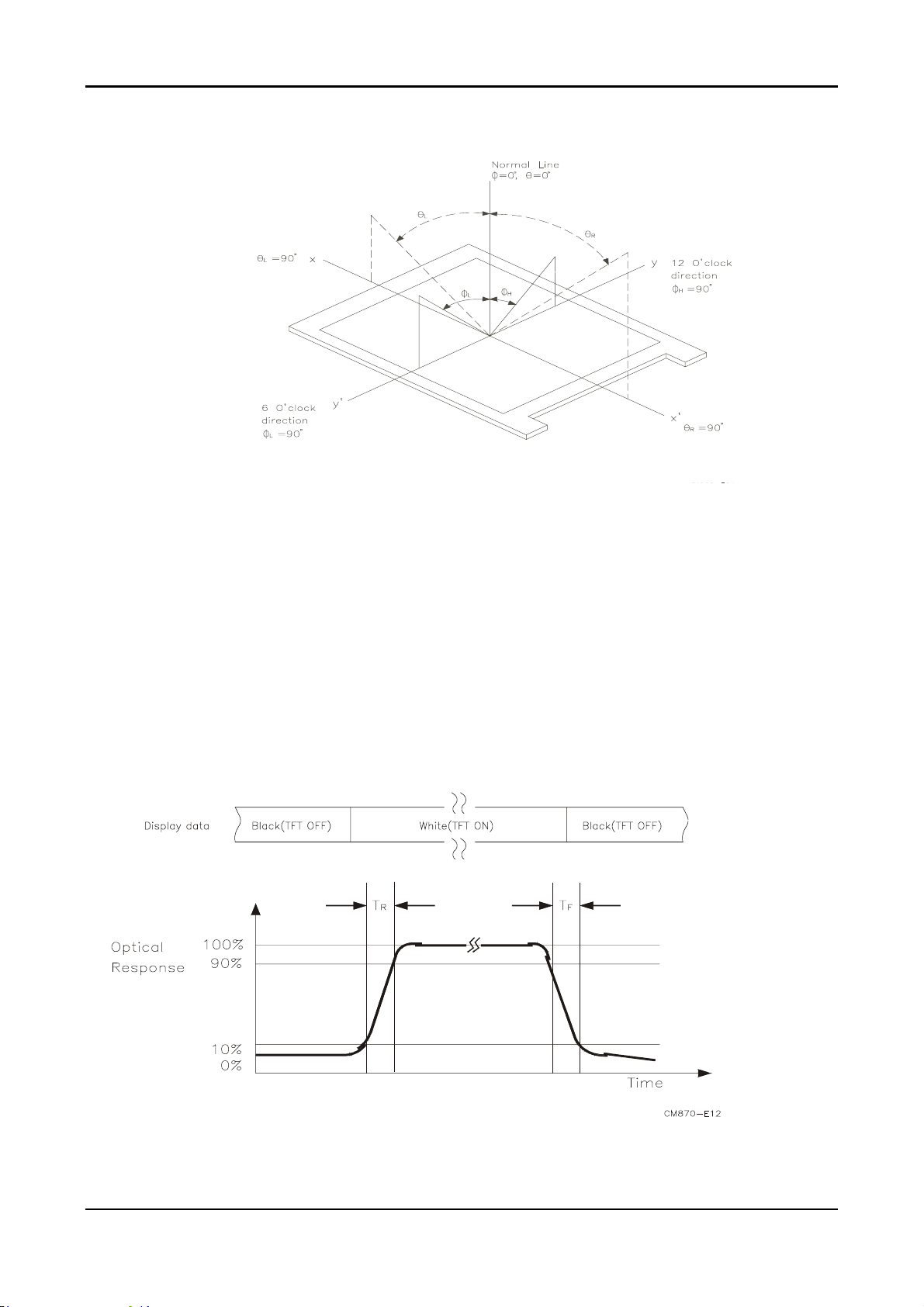
• Optical Specifications
The following items are measured under stable conditions. The optical characteristics
should be measured in a dark room or equivalent state with the methods shown in
Note(4).
Measuring equipment : TOPCON BM-5A, BM-7, PHOTO RESEARCH PR650
(Inverter Freq. : 54kHz) *Ta =25 ± 2°C, VDD=5V, fv=60 Hz, fDCLK=54 MHz, IL= 6.5mArms
ITEM Symbol Condition MIN. TYP. MAX. UNIT
Contrast Ratio
(Center of screen)
Rising T
Time at Ta
Falling T
Luminance of white
(Center of screen)
Red
Color
Green
Chromaticity
(CIE)
Blue
White
Viewing
Angle
Hori.
Vert.
Brightness Uniformity B
Flicker F - - 5 %
Cross talk C
CR
R
F
Y
L
φ=0,
R
X
R
Y
G
X
GY 0.568 0.598 0.628
θ=0
Normal
Viewing
Angle
BX 0.115 0.145 0.175
BY 0.073 0.103 0.133
WX 0.270 0.300 0.330
WY
θL
θR
φ
φ
UNI
H
L
T
CR≥10
350 430
-
-
5 Response
15
250
-
30
-
(total)
msec
cd/m
2
0.599 0.629 0.659
0.324 0.354 0.384
0.257 0.287 0.317
0.305 0.335 0.365
- 80 -
- 80 -
Degrees
- 65 -
- 65 -
- - 1.2
- - 20 %
*For Edge shadow will follow limit sample to check.
6
Page 8
Note 1) Definition of Viewing Angle: Viewing angle range (10≤CR)
Note 2) Definition of Contrast Ratio (CR): Ratio of gray max(Gmax),gray min(Gmin) at the
center point of panel.
Luminance with all pixels white (Gmax)
CR=
Luminance with all pixels black (Gmin)
Note 3) Definition of Response time: Sum of TR , TF
Note 4) After stabilizing and leaving the panel alone at a given temperature for 30 min,
the measurement should be executed .Measurement should be executed n a
stable, windless ,and dark room.30 min after lighting the back-light. This
should be measured in the center of screen. Dual lamp current :13.0mA(6.5mA
7
Page 9
x2)(Refer to the note(1) in the page 14 for more information ).
Environment condition :Ta=25±2°C
Optical characteristics measurement setup
Notes 5) Definition of Luminance of White : measure the luminance of white at center point.
8
Page 10
○ is test point.
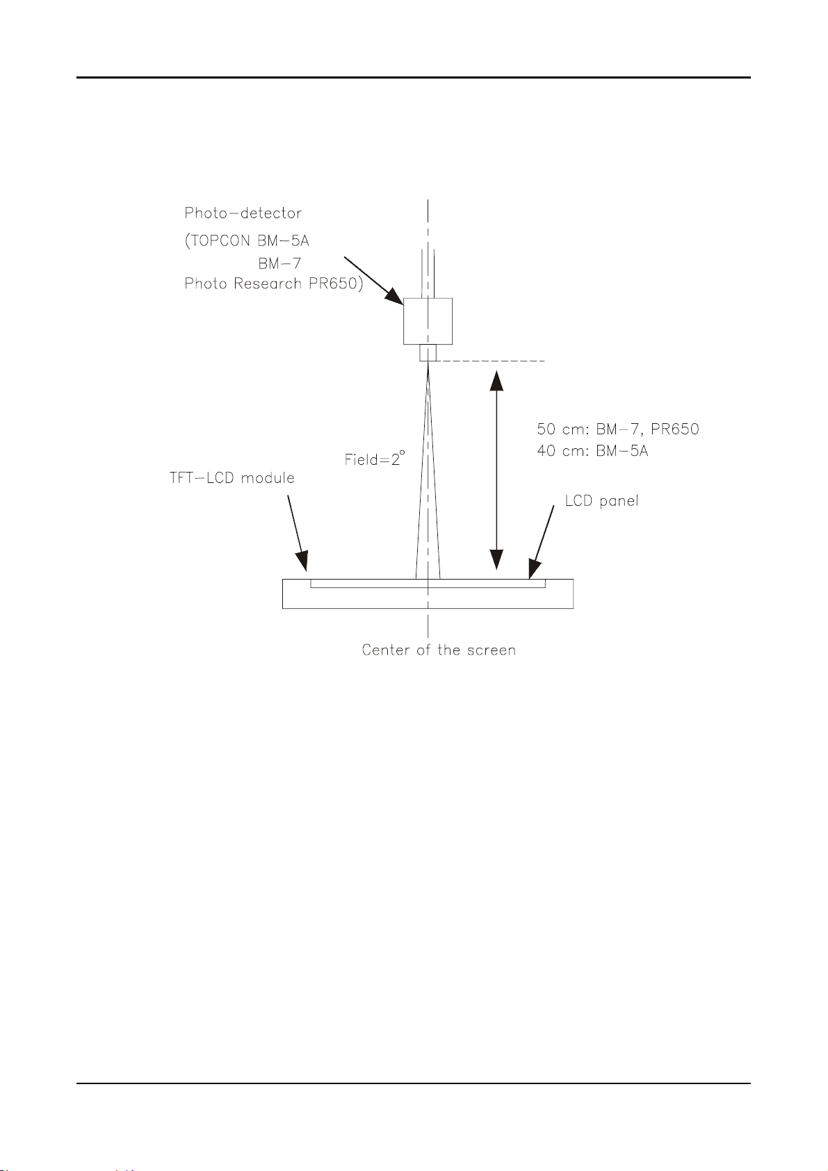
Notes 6)Definition of 9 points brightness uniformity (Measuring points: Refer to the Note 5)
Bmin
B
=100∗
UNI
Bmax
Bmax: Maximum brightness
Bmin: Minimum brightness
Notes 7) Definition of Flicker level
Flicker Voltage
pp
F = x 100 %
LMD Voltage
dc
♦ One maximum value of three estimated values.
♦ For this test ,an LMD(Light Measurement Device)is needed with adequate response time
to track any visible rate flicker component and with a voltage level output proportional
To luminance intensity.
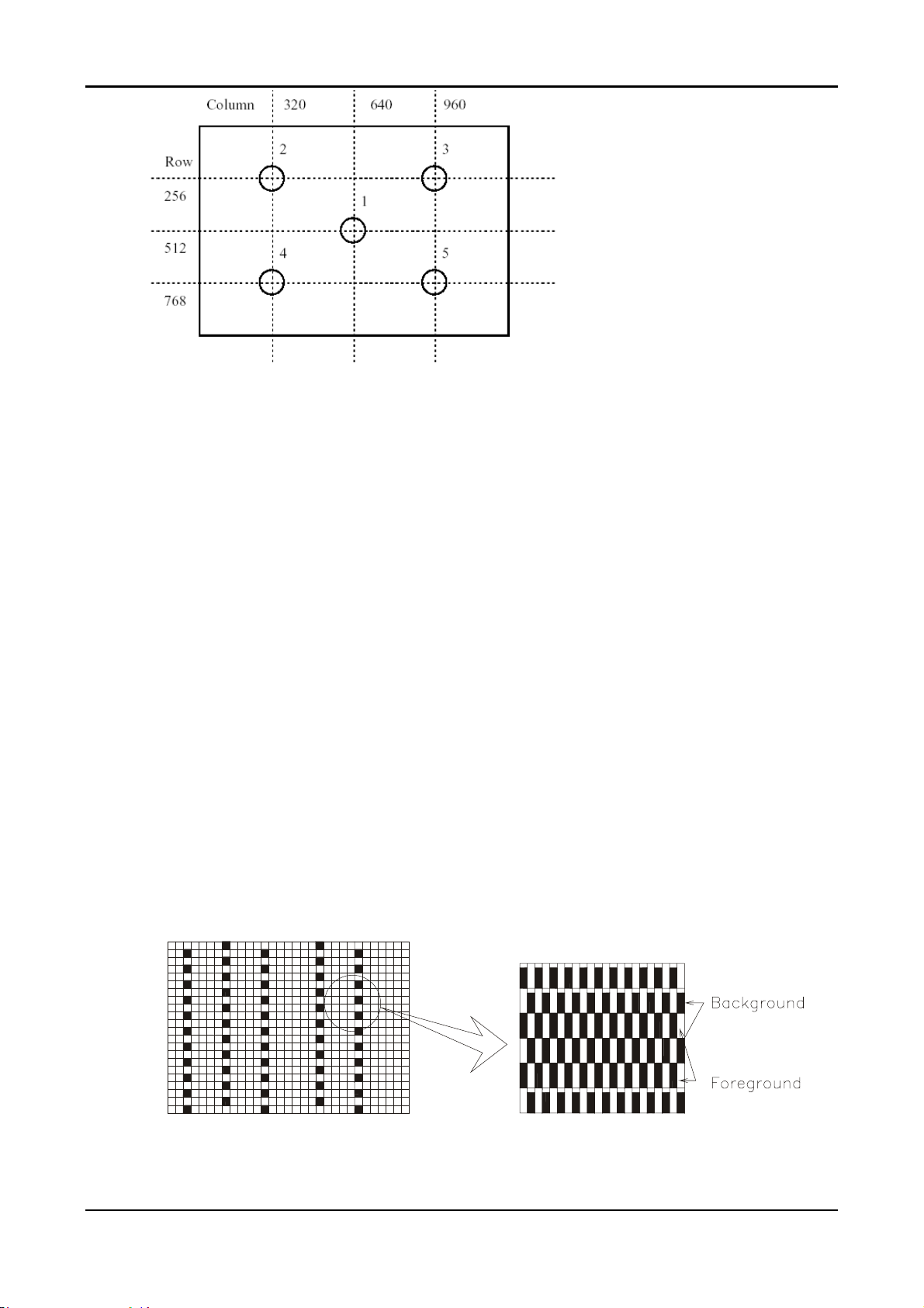
♦ Test Pattern: For dot inversion Driving(Gray levels of foreground dots on the test panel
Are G22,G32,and G45)
♦ Test Point :Center point of the display area
9
Page 11
Note 8) Definition of Crosstalk (Refer to the VESA STD)
The calculation for shadowing is made from the 2 luminance measurements Gbkg and Lsh,
as follows:
Lmax -Lmin
C
= x100 %
T
Lmin
Where Lmax is the larger value of Gbkg or Lsh , and Lmin is the smaller of the two.
♦ To determine background and foreground levels (colors),first set the background to any
gray scale or color level suitable for shadowing determination.(Note that it may take
several iterations of adjusting background level and box levels to determine the proper
value for the background .Next display the box levels to determine the proper value for the
background level. Look for shadowing in any direction from box E. Independently vary the
gray level (or color) of the background and box E until the worst case shadowing is
observed. This defines the background (Gbkg) and foreground (Gfg) levels to be
maintained for the remainder of the test.
♦ One point only (the target) will be measured. To determine that point proceed as follows
Using the background and foreground gray levels of step1 (Gbkg and Gfg). Turn on each
box at a time. Look for the case with the worst shadowing. The box causing the worst case
is the shadowing source, or Bsrc. Use Bsrc and the box opposite from it that lies directly in
the shadow path. That is the target box, or Btgt. Note that box Eight be either Bsrc or Btgt,
depending on the shadowing conditions, but typically Bsrc and Btgt will be a pair of
opposite boxes, A&C or B&D. Btgt will only be displayed for aligning the LMD. It will be
turned off for the actual measurement.
♦ The target box point (Btgt) will be measured with the source box (Bsrc) turned on then off.
(Btgt is for alignment purpose only) Display the background only at level Gbkg. Display
Btgt determined in step 2 above. Using the correct distance, angle, and measurement
aperture, align the LMD to the center of the Btgt. Turn off Btgt. With Gbkg set to its proper
level, measure the luminance (or color). Next,turn on the source box Bsrc. Again measure
at the center point of Btgt (without Btgt present.). In this case the LMD will be measuring
the shadowing level, Lsh.
10
Page 12
2.4 Input Signals
2.4.1 Video input
• Type Analog R, G, B., Digital TMDS
• Input Impedance 75 ohm +/- 2%
• Polarity Positive
• Amplitude 0 - 0.7 +/- 0.05 Vp
• Display Color same as LCD panel
2.4.2 Sync input
• Signal separate horizontal and vertical sync, or composite sync
which are TTL compatible
• Polarity positive and negative.
2.4.3 Interface frequency
The following frequency range is generalized by supported timing. If the entered
mode does not match the supported timing the display optimization will not be
assured.
• Horizontal Frequency 30KHz --80KHz(analog), 31.5– 64KHz(digital)
• Vertical Frequency 56Hz ---------75Hz
DISPLAY MODES
MONITOR
MODE NO.
1 640X480 31.5 - 60.0 - 25.0 Defacto
2 640X480 37.86- 72.80- 31.5 VESA
3 640X480 37.5- 75.0- 31.5 VESA
4 720X400 31.5 - 70.0 + 28.0 Text Defacto
5 800X600 37.8 + 60.0 + 40.0 VESA
6 800X600 48.07 + 72.18 + 50.0 VESA
7 800X600 46.87+ 75.0+ 49.5 VESA
8 1024X768 48.4 - 60.0 - 65.0 VESA
9 1024X768 56.47 - 70.07 - 75.0 VESA
10 1024X768 60.0 + 75.0 + 78.75 VESA
11 1280X1024 64.0 + 60.0 + 108.5 SXGA
12 1280X1024 80.0 + 75.0 + 135.0 SXGA
SCREEN
RESOLUTION
HORIZONTAL
SYNC RATE
(kHz)
VERTICAL
SYNC RATE
(Hz)
VIDEO CLK
(MHz)
STANDARD
11
Page 13
Supported Timing
TIMING FH(KH
FV(HZ) POLARITY (DOT/LINE) (DOT/LINE) WIDTH PORCH PORCH FOREQ.(MHZ)
(DOT/LINE) (DOT/LINE) (DOT/LINE)
640x480 31.469 – 800 640 96 16 48 25.175
VGA-480 59.94 – 525 480 2 10 33
640x480 37.861 – 832 640 40 16 120 31.5
VESA-480-72Hz 72.809 – 520 480 3 1 20
640x480 37.5 – 840 640 64 16 120 31.5
VESA-480-75Hz 75 – 500 480 3 1 16
720x400 31.469 – 900 720 108 18 54 28.322
VGA-400-TEXT 70.087 + 449 400 2 12 35
800x600 37.879 + 1056 800 128 40 88 40
VESA-600-60Hz 60.317 + 628 600 4 1 23
800x600 48.077 + 1040 800 120 56 64 50
VESA-600-72Hz 72.188 + 666 600 6 37 23
800x600 46.875 + 1056 800 80 16 160 49.5
VESA-600-75Hz 75 + 625 600 3 1 21
1024x768 48.363 – 1344 1024 136 24 160 65
XGA 60.004 – 806 768 6 3 29
1024x768 56.476 – 1328 1024 136 24 144 75
VESA-768-70Hz 70.069 – 806 768 6 3 29
1024x768 60.023 + 1312 1024 96 16 176 78.75
VESA-768-75Hz 75.029 + 800 768 3 1 28
1024x1024 64 + 1688 1280 112 48 248 108
VESA-1024-60Hz 60 + 1066 1024 3 1 38
1280x1024 80 + 1688 1280 144 16 248 135
VESA-1024-75Hz 75 + 1066 1024 3 1 38
If the input timing is not a supported timing listed above but within the supported frequency
range (Horizontal: 80KHz,Vertical: 75Hz), this monitor will select a closest mode instead. But
the display quality may not be optimized.
If the input timing over the supported frequency range, a message “Input Signal Out of Range”
will be shown.
SYNC TOTAL ACTIVE SYNC FRONT BACK PIXEL
Z)
2.4.4 Support Modes
There will be 12 total support modes to accommodate the above mode and other video
modes within the frequency range of the monitor.
Analog R, G, B. MAX supports range 1280x1024 75Hz.
Digital TMDS MAX supports range 1280x1024 60Hz.
12
Page 14
2.4.5 85Hz refresh rate Support
Monitor should display 85Hz refresh rate mode as emergency mode.
Monitor should display “Out of Range” warning menu at this mode.
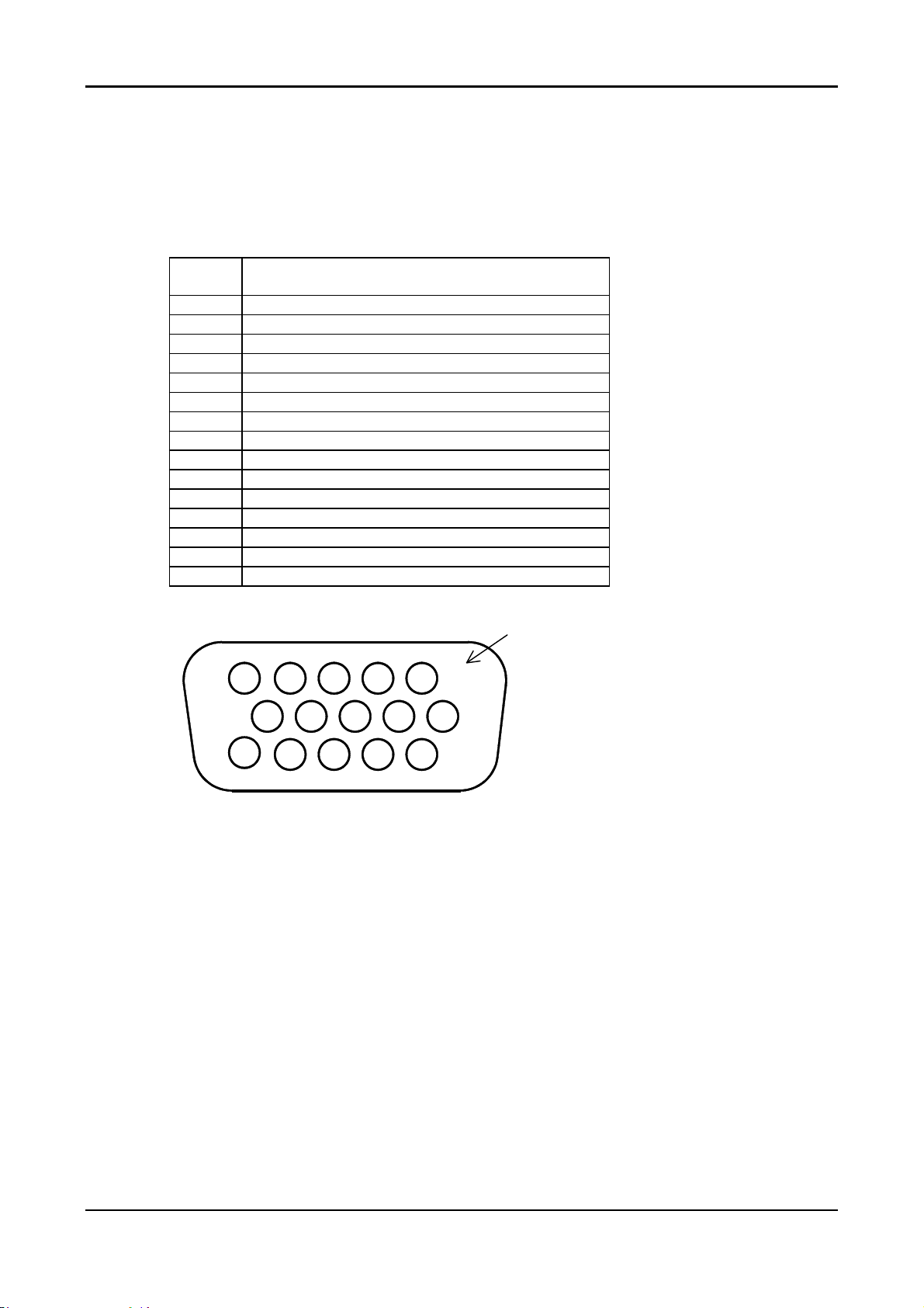
2.4.6 Analog Video input Connector
Analog Video input Connector: 15pins mini D-Sub
Table 2.4.5. Pin assignment for D-sub connector
PIN
NO.
1 RED VIDEO
2 GREEN VIDEO
3 BLUE VIDEO
4 GROUND
5 GROUND
6 RED GROUND
7 GREEN GROUND
8 BLUE GROUND
9 PC5V (+5V DDC)
10 CABLE DETECTION
11 GROUND
12 SDA
13 H.SYNC
14 V.SYNC
15 SCL
Separate Sync
Color of plastic parts: Blue
5 1
10
15
D-sub connector
6
11
13
Page 15
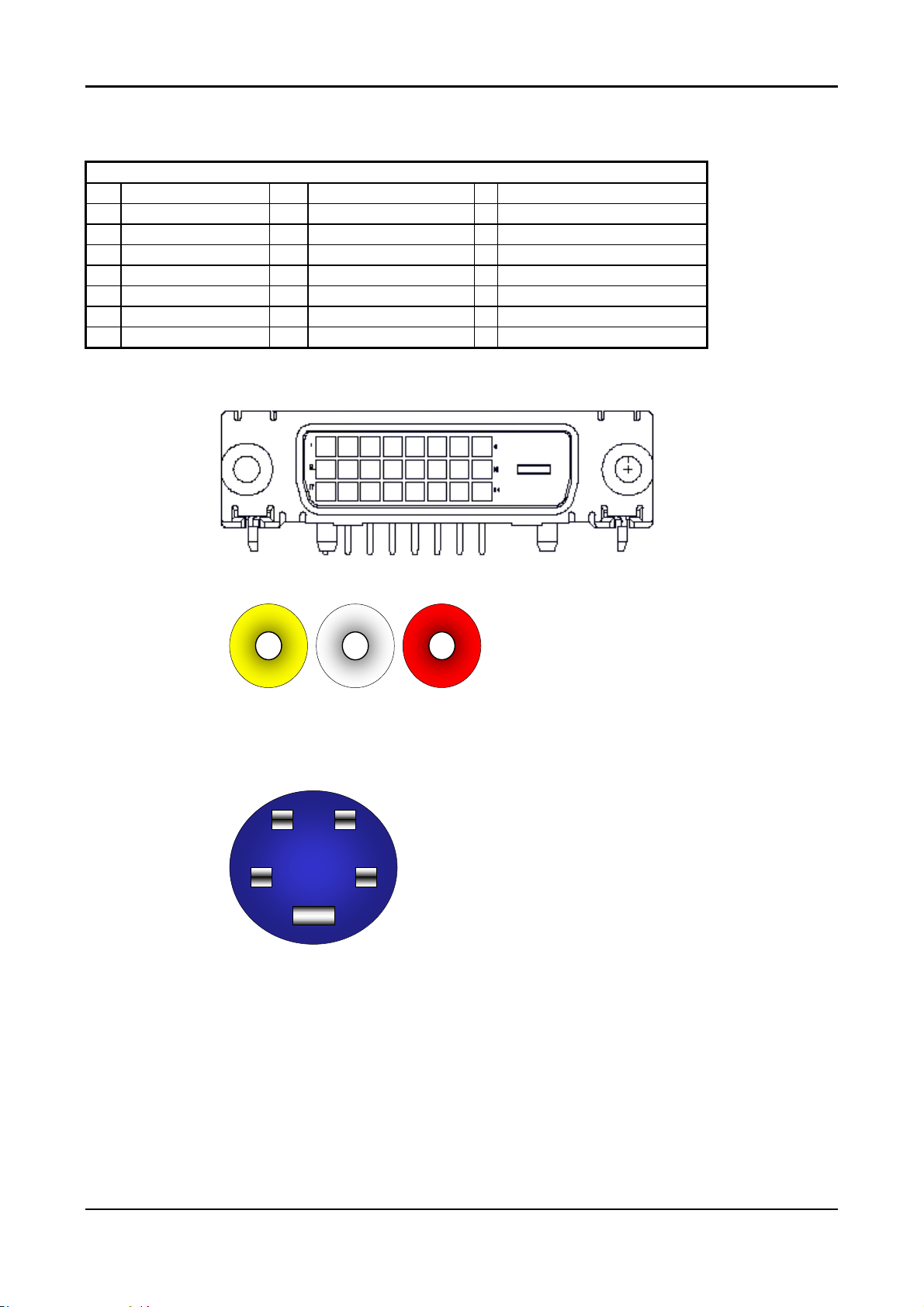
Digital Video input Connector: DVI-D (T.B.D)
Table 4-3-3. Pin assignment for DVI-D (24pin) connector
Pin – Assignment of DVI –D connector :
1 TX2- 9 TX1- 17 TX0-
2 TX2+ 10 TX1+ 18 TX0+
3 Shield (TX2 / TX4) 11 Shield (TX1 / TX3) 19 Shield (TX0 / TX5)
4 NC 12 NC 20 NC
5 NC 13 NC 21 NC
6 DDC-Serial Clock 14 +5V power *) 22 Shield (TXC)
7 DDC-Serial Data 15 Ground (+5V) 23 TXC+
8 No Connect 16 Hot plug detect 24 TXC-
*) In case, the power of the PC unit is switched off and the power of the monitor is switched on,
no voltage may occur at pin 14.
Composite Video: Monitor rear side RCA female (Yellow).
AV1-input
S-Video (Y/C): Monitor rear side 4 Pin Mini-DIN female.
S-Video
2.4.7 Support Composite Video & S – Video Input:
JV3 for Composite Video RCA female (Yellow)
JV4 for S-Video female (Black)
Composite/S-VIDEO INPUTS
S-Video Type Y/C : NTSC/PAL
Level 0.7Vpp
14
Page 16
Impedance 75 ohm terminated
Composite Video Type Composite : NTSC/PAL
Level 0.7Vpp
Impedance 75 ohm terminated
2.5 CONTROLS
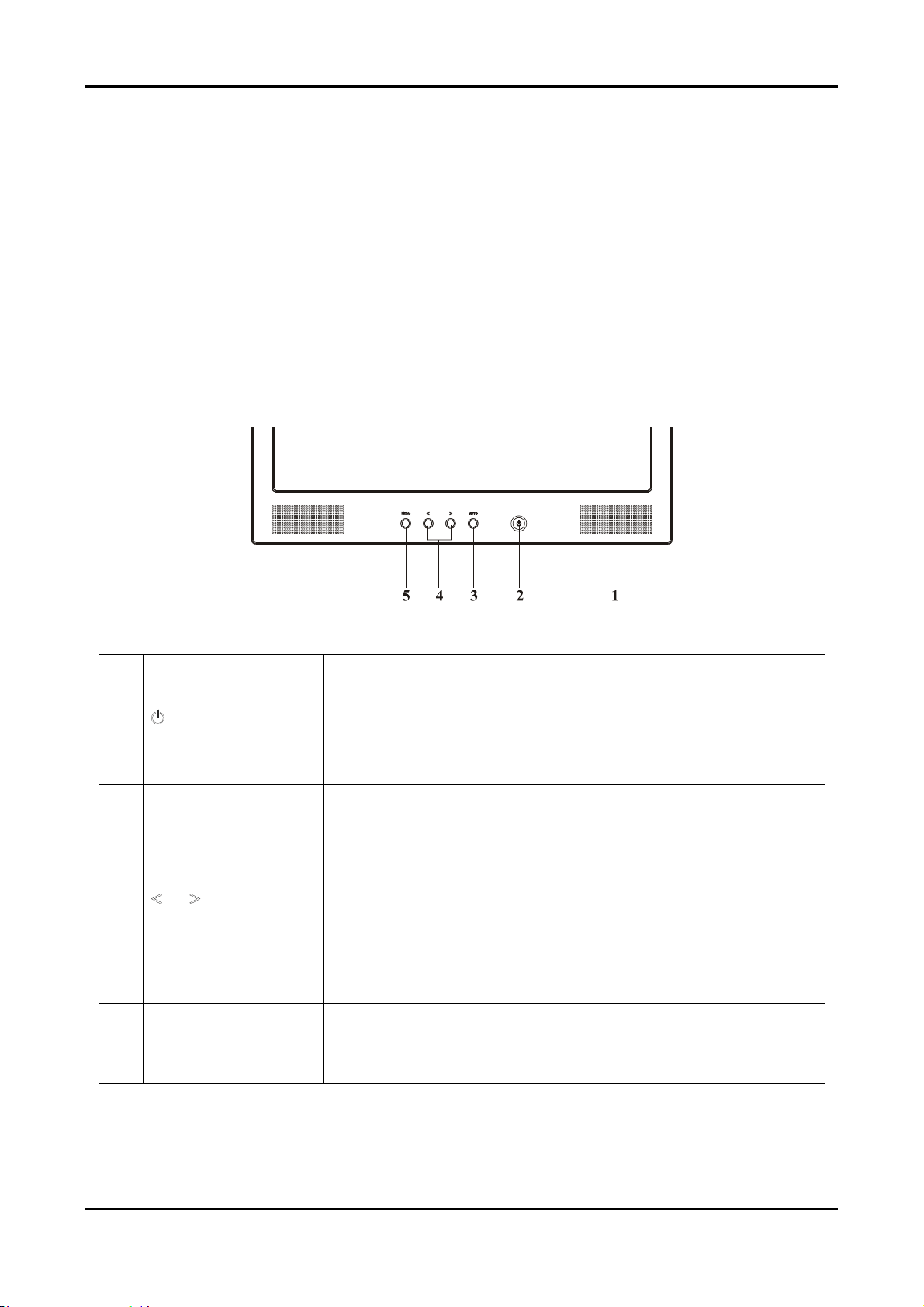
A brief description and the location of all LCD Monitor functions controls and indicators:
1
2
3 Auto
4
5 Menu
Stereo Speakers
Soft Power Switch
(DC Power-On
Indicator)
Function Select and
Adjustment Control
Buttons
Figure 2-1
PC Audio Stereo output.
1. Press the soft power switch to switch the monitor ON/OFF.
2. LED lights Blue color --- Power is ON.
3. LED lights Yellow --- Monitor is in "Power Saving Mode".
4. LED is off --- Power is OFF.
1. Press the Auto Buttons Monitor will Auto-Adjusting.
2. Press the Auto Buttons over 2 second the Monitor Searching next
source.
1. Direct press either left or right control button can adjusting speaker
Volume control.
2. When press after Menu buttons then Press either left or right control
button for OSD first menu (left side) function selection.
1. When selection you want adjusting function then press Menu
buttons again for OSD second menu (right side) function selection.
You can Press the left button to decrease the OSD setting and press
the right button to increase the OSD setting.
1. Press the Menu will show OSD (On Screen Display) Function
Menus table.
2. When OSD (On Screen Display) Menus display press Menu
Buttons will enable selection function.
15
Page 17
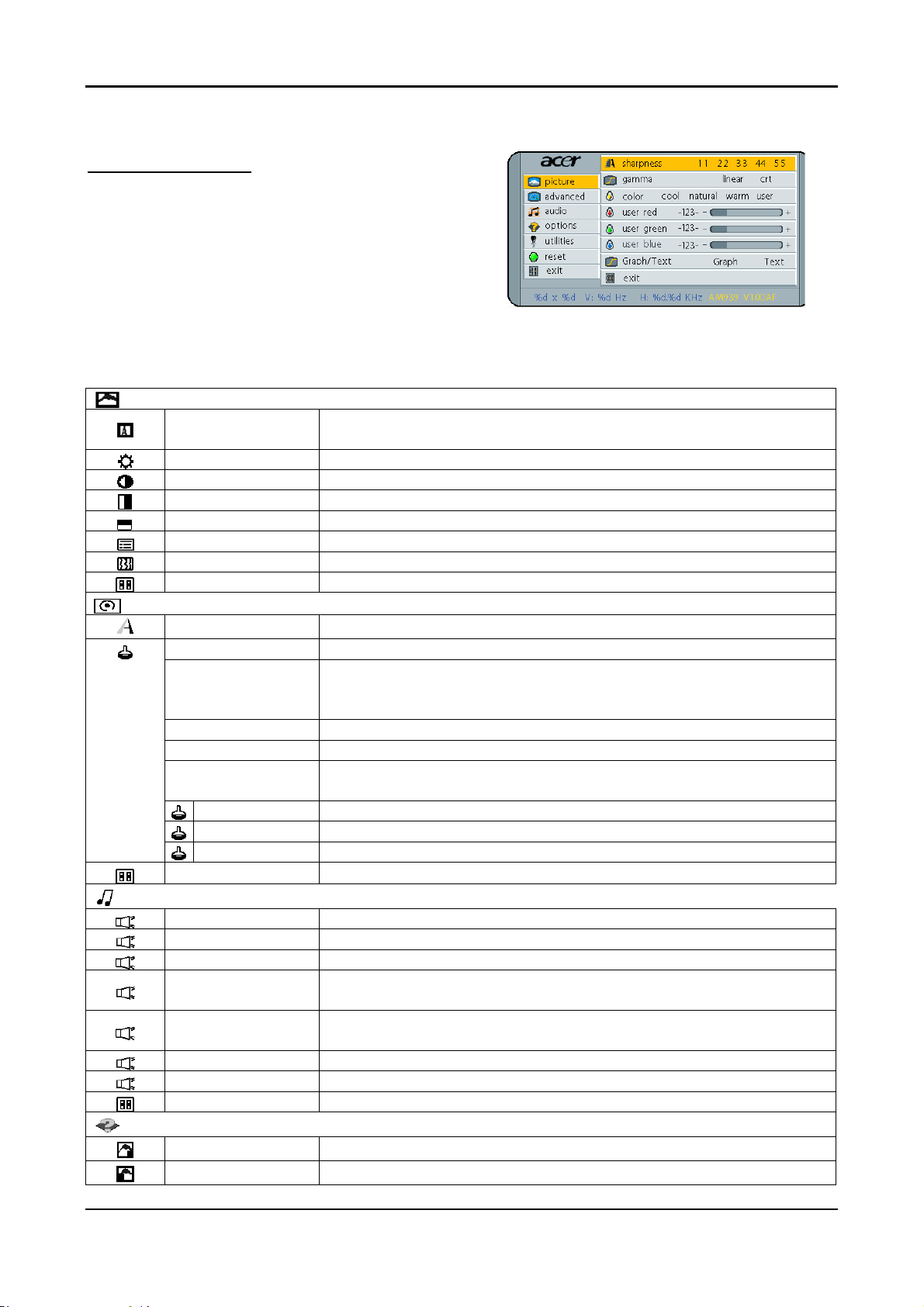
2.5.1 Adjusting the Monitor’s Display
The monitor has four function control buttons to select among functions shown on OSD menu,
designed for easy user-viewing environments.
OSD Function Menu
To access OSD Main menu, simply press one of the
Function Select control buttons, and the menu diagram will
pop up on the screen as shown on Fig. 2-2:
Continue pressing the Function Select buttons to scroll
through the entire menu items ,then press Adjustment
Control buttons to adjust content of selected item.
Figure 2-2
2.5.2 Function Description
2.5.2.1.1.1 Analog RGB / Digital RGB
Picture
Advanced
Audio
Options
Auto adjust
Brightness Adjust the overall image and background screen brightness.
Contrast Adjust the image brightness in relation to the background.
H-position To move the picture image horizontally left or right.
V-position To move the picture image vertically up or down.
Phase To improve focus clarity an image stability.
Clock To increase or decrease the horizontal size of image.
Exit To exit the main menu.
Sharpness Adjusts the picture sharpness.
Color You have 4 kinds of options.
Cool
Natural This performance is reddish and closer to paper white.
Warm This performance is yellowish and closer to paper white.
User
User red Increase or decrease red.
User green Increase or decrease green.
User blue Increase or decrease blue.
Exit To exit the main menu.
Volume This features adjusts < to decrease volume and > to increase volume.
Base This features adjusts < to decrease base and > to increase base.
Treble This features adjusts < to decrease treble and > to increase treble.
ATTL
ATTR
Loudness This features choose on or off to get loudness.
Mute This features choose on or off to mute the sound.
Exit To exit the main menu.
OSD To move the OSD image.
OSD H-position To move the OSD image horizontally left or right.
Press > button, auto adjust the display mode to its utmost performance
according to VGA setting.
This control adjusts the color temperature of the screen image, this item
are preset by factory, you can not adjust these setting, The performance is
bluer and brighter.
You can adjust the individual color intensity by yourself. Increase or
decrease red, green or blue depending upon which is selected
This features adjusts < to decrease left speaker volume and > to increase
left speaker volume.
This features adjusts < to decrease right speaker volume and > to increase
right speaker volume.
16
Page 18
OSD V-position To move the OSD image vertically up or down.
Language You can choose one of the nine languages you need.
Exit To exit the main menu.
You can select how long the monitor waits after the last adjust of the key
OSD timeout
OSD background You can select opaque or translucent to change OSD background.
Source icon You can select on or off to display OSD icon.
Exit To exit the main menu.
Memory recall
Exit To exit the menu.
Composite Video / S-Video
Brightness Adjust the overall image and background screen brightness.
Contrast Adjust the image brightness in relation to the background.
Saturation Adjusts the color saturation of the screen image.
Hue Adjusts the color hue of the screen image.
Sharpness Adjusts the picture sharpness.
Scaling Adjusts the picture size full screen or 16:9 screen.
Exit To exit the main menu.
Sharpness Adjusts the picture sharpness.
Color You have 4 kinds of options.
Cool
Natural This performance is reddish and closer to paper white.
Warm This performance is yellowish and closer to paper white.
User
User red Increase or decrease red.
User green Increase or decrease green.
User blue Increase or decrease blue.
Exit To exit the main menu.
Volume This features adjusts < to decrease volume and > to increase volume.
Base This features adjusts < to decrease base and > to increase base.
Treble This features adjusts < to decrease treble and > to increase treble.
ATTL
ATTR
Loudness This features choose on or off to get loudness.
Mute This features choose on or off to mute the sound.
Exit To exit the main menu.
to shut off the OSD menu. The time setting choices are from 5 to 60
seconds.
Reset the currently highlight control to the factory setting. User must be
using factory preset video mode to use this function.
To exit the OSD menu.
This control adjusts the color temperature of the screen image, this item
are preset by factory, you can not adjust these setting, The performance is
bluer and brighter.
You can adjust the individual color intensity by yourself. Increase or
decrease red, green or blue depending upon which is selected
This features adjusts < to decrease left speaker volume and > to increase
left speaker volume.
This features adjusts < to decrease right speaker volume and > to increase
right speaker volume.
Utilities
Reset
Exit
Picture
Advanced
Audio
Options
17
Page 19
Utilities
Reset
Exit
OSD To move the OSD image.
OSD H-position To move the OSD image horizontally left or right.
OSD V-position To move the OSD image vertically up or down.
Language You can choose one of the nine languages you need.
Exit To exit the main menu.
You can select how long the monitor waits after the last adjust of the key
OSD timeout
OSD background You can select opaque or translucent to change OSD background.
Source icon You can select on or off to display OSD icon.
Exit To exit the main menu.
Memory recall
Exit To exit the menu.
to shut off the OSD menu. The time setting choices are from 5 to 60
seconds.
Reset the currently highlight control to the factory setting. User must be
using factory preset video mode to use this function.
To exit the OSD menu.
Sharpness : Adjust the scale-up effect(smoother or sharper.)
OSD Transparency: Adjust the transparency level of OSD. The range is from 0 to 100 scales.
Comment:
• 1280x1024: Current mode resolution.
• 60 HZ: Current mode vertical frequency±1Hz.
• VER 1.00: Firmware revision.
Other features:
Intellectual-Auto AM737 can start the Auto-Adjustment automatically when input a new
display mode at first time less then 4 sec to finish. After the adjustment, AM737 will
remember this mode and switch to optimized condition automatically for this mode
whenever encounter this mode again.
The 640×400, 720×400 mode can do graph/ text select on OSD Advanced function.
Total 13 recent used modes are recorded into EEPROM. If other support modes input to
monitor EEPROM will cancel by first in first out motion.
After finishing adjustment from OSD, the data need 3 sec to save NVRAM memory.
VESA DPMS Functionality When signaled by the host CPU, AM737 show a black
screen about 5 seconds. If no further signal, then it shows “No Signal” and enter power
saving mode.
18
Page 20

2.6 White Color Temperature
White color temperature is 4 preset as 9300, 7500,6500 and User,
Default value of user color should be user which is maximum setting for panel.
Target of color setting
Color Temp. Color Coordinate Tolerance Color Coordinate Tolerance
x y u’ v’
Cool (9300K) 0.283 0.297 +0.03 0.189 0.446 u’v’ < 0.01*
Natural (6500K) 0.313 0.329 +0.01 0.198 0.468 u’v’ < 0.01*
Warm (5000K) 0.346 0.359 +0.03 0.209 0.488 u’v’ < 0.01*
User - - - - -
*) TCO’0X A.2.6.1 requirement
User should follow “Microsoft Windows Color Quality Specification for Liquid Crystal Display OEM’s”.
(http://www.microsoft.com/hwdev/tech/color/ColorTest.asp
)
19
Page 21
2.7 POWER SUPPLY
(PK10V000020, LAE LAD6019AB5 BLK 90D)
(PK10V000030, LAE LAD6019AB5 IVO 90D)
( PK10V000040, LSE0218B1260 BLK 90D)
(PK10V000050, LSE0218B1260 IVO 90D)
2.7.1 input Voltage Range
The monitor shall operate within specification over the range of 90 to 265 VAC power supply.
2.7.2 Input Frequency Range
Input power frequency range shall be from 47.5 to 63 Hz over the specified input
voltage range.
2.7.3 Quick specification review
• Input current 1.2A (max) at 90VAC input and full load ,
0.6A (max) at 264 VAC input and full load.
• Inrush current @ cold start
30A(0-peak)@ 110Vac ,50A(0-peak) @ 220Vac
(measured when switched off for at least 10 mins.)
• Output
Tolerance Output Current
Output Volt - MIN MAX
+12Vdc
• Total output power: 60 Watt max.
• Withstanding voltage : 1.5Kvac or 2.2KVdc for 1 minute.
• Leakage current : < 0.25mA/100Vac , <3.5mA/230Vac
• Efficiency : 80% min. @115V/230VAC, maximum load.
2.7.4 Power Management
2.7.4.1 Meet VESA DPMS proposal
The monitor must comply with the Microsoft On Now specification, with a minimum of three power
management states, as defined by the VESA DPMS document. The front panel of the monitor must
appropriately display the DPMS state, For example:
±5%
Volt Tolerance
0A 5A 11.4~12.6Vdc
DPMS ON : The power LED is Blue
DPMS OFF : The power LED is Amber
2.7.5 Power Consumption
On mode 55 Wmax Green
Off mode 5 Wmax Amber
DC power off 5 Wmax Dark
disconnection 5 Wmax
Power saving states are measured with speakers attached but not worked.
The recovery time from stand by /suspend/off mode to on mode is 3 seconds maximun.
Dark (DC power off)
Amber (DC power on)
20
Page 22
2.7.6 Power Connector
All units shall have an IEC/CEE-22 type male power receptacle.
2.7.7 Inverter & DC/DC Board (VP-903)
1.Hydis / HT17E12-200 (Condition:Ta=25 )℃
No. Item Sym Condition Min Typ. Max. Unit
Input Voltage Vin 11.4 12 12.6
1
Lamp Voltage VLamp Vin=12V,ILAMP= 7.5mA - 700 -
2
Luminance Bmax Center of screen, 6.5mA for
3
Working Frequency Fo 40 60
4
Lamp Current ILAMP 3 6.5 6.9
5
Backlight ON/OFF
Control
6
Brightness control
7
range(positive
adjustment)
Lamp Current Balance
8
, each two output of
transformer
Open Lamp Volt. Vopen Vin=12V, 0degC 1600 - --
9
ON Normal Operation 1.5 3.3
OFF Shutdown (Lamp off) 0 1.0
0 - 3.1
IL1-IL2 Two output of one
each lamp.
transformer
250 -
+/-0.5
V
Vrms
cd/m^2
KHz
mA
V
V
V
mA
Vrms
10
Efficiency
Strike Lamp time
11
Delay Time for Open
Lamp Protection
12
/each lamp
Audible Noise
13
2.Pin Assignments
2-1 Output Connector#1 (J802 / E&T 4500-09 / 9P P2.0)
Pin No.
1
2
3,4
5
6
7,8
9
- Vin=12V,maximum brightness 75 - -
Ts Vin=12V, ON/OFF=0V 40 60 80
Topen
Symbol
+5Vaudio
GND/Audio
GND
Brightness
Enable
Vcpu
Vcc
Vin=12V, each lamp is
disconnected
30mm upon the part - - 34
-- 1000
Description
+5Vdc for Audio ckt
Ground for Audio ckt
Common Ground
Brightness adjustable range: 0 V<min> ~ 3.1V<max>
Backlight ON/OFF control (Active High)
ON:1.5~3.3V, OFF:-0.3~1.0V
+5Vdc supply to micro-P, always on.
+12 Vdc supply to mainboard.
%
ms
ms
dBm
2-2. Output Connector#2 (for CCFLs , J940,J980,J941,J981)
21
Page 23

Connector type: ACES 87210-0236 P3.5 or alternative
Pin No. Symbol Descripition
1 HV High Voltage
2 LV Low Voltage
2.8 Plug & Play (EDID)
The monitor will be capable of sending a VESA standardized EDID file through the DDC (pins 12,
15 of the VGA connector).
22
Page 24
2.9 Audio Technical specification
2.9.1 General Description:
Output power : 1Wrms + 1Wrms maximum
Total harmonic distortion : Less than 1 % (except speakers distortion)
Input signal sensitivity : 0.5 Vrms for full output
Input impedance : 47 Kohm +/- 5 %
Frequency response range : 20Hz – 20kHz (except speakers response)
Difference of L and R output : Less than 2 dB
2.9.2 Electrical characteristics (Tamb=25°)
Audio amplifier(USE Panasonic VP-7723A Audio Analyzor. )
Spec. Item Audio Input Freq.
Comment
Min. Typ. Max.
Input Voltage(V) - 5 -
Input Current(m A) - 500 800
Audio Voltage Gain 500m Vrms 1KHz - - 6 d B Volume Max.,load 4 Ω
Frequency Response 500m Vrms 300Hz-20KHz -10dB - +10d B Volume Max.,load 4 Ω
Signal to Noise ratio 500m Vrms 1KHz - - -40dB Volume Max.,load 4 Ω
Total harmonic distortion 500m Vrms 1KHz 1% except speakers distortion
Cross talk 500m Vrms 1KHz - - -30dB Volume Max.,load 4 Ω
Output Watt. 500m Vrms 1KHz - - 1W Volume Max.,load 4 Ω
Volume Control - - - Analog
2.9.3 Speakers
Maximum power : 2 W speaker(max)
Impedance : 4 ohm +/- 15 % @ 1kHz 1.0Hz
Frequency response range : 350 Hz – 15 kHz (S.P.L. – 10 dB)
Total harmonic distortion : Less than 5 % @ 0.125 W 1kHz
23
Page 25

3. VL-903 DISPLAY CONTROL BOARD
3.1 Description
The VL-903 display control board is design to directly convert the analog RGB signals from
standard VGA display card to optimum LCD timing signals so as to construct a high display
quality LCD monitor.
3.2 Features
On board embedded micro-processor to detect display timings and control user
•
functions.
• Using PixelWorks PW131 design to generate optimum LCD timings.
2
• Using E
• Support up to 13 display modes from VGA to SXGA.
• Offer full screen expansion function on non-SXGA mode (automatic).
• Flexible color temperature selection function including Cool = 9300, Natural = 6500,
Warm = 7500 and user mode color temperature.
PROM to memorize every adjusted parameter.
• Support OSD functions.
• Support VESA DPMS function.
• Support DDC2B functions.
• Support 8 languages for OSD description.
• The longest time for mode change is 7 seconds.
24
Page 26

3.3 BLOCK DIAGRAM
25
Page 27

3.4 Connector Locations
3.5 Connector Type
Location Type Maker Number of pins
CN1 24P Female V/DVI-D Foxconn 24
CN2 15P Female V/D-Sub E&T 15
CN3 4300-04 E&T 04
CN5 98210-4011 E&T 40
CN6 4500-09 E&T 09
CN8 4300-05 E&T 05
CN10 4300-08 E&T 08
26
Page 28

3.6 Connector pin assignment
3.6.1 CN2
Pin NO. Signal Comment
1 R-Video Red Video Input.
2 G-Video Green Video Input.
3 B-Video Blue Video Input.
4 N. C.
5 Ground Ground.
6 Ground Ground.
7 Ground Ground.
8 Ground Ground
9 5VCC DDC Power Input.
10 PCDETECT PCDETECT Input.
11 NC NC
12 SDA DDC 2B
13 HS Horizontal Sync Input.
14 VS Vertical Sync Input.
15 SCL DDC 2B
3.6.2 CN5
Terminal No. Symbol Function
36,37,38 VDD 5V POWER SUPPLY
10 TXECLK- LVDS EVEN OUTPUT DATA PAIRS
11 TXECLK+ LVDS EVEN OUTPUT DATA PAIRS
13 TXE3- LVDS EVEN OUTPUT DATA PAIRS
14 TXE3+ LVDS EVEN OUTPUT DATA PAIRS
16 TXO0- LVDS ODD OUTPUT DATA PAIRS
17 TXO0+ LVDS ODD OUTPUT DATA PAIRS
19 TXO1- LVDS ODD OUTPUT DATA PAIRS
20 TXO1+ LVDS ODD OUTPUT DATA PAIRS
22 TXO2- LVDS ODD OUTPUT DATA PAIRS
23 TXO2+ LVDS ODD OUTPUT DATA PAIRS
25 TXOCLK- LVDS ODD OUTPUT DATA PAIRS
26 TXOCLK+ LVDS ODD OUTPUT DATA PAIRS
28 TXO3- LVDS ODD OUTPUT DATA PAIRS
29 TXO3+ LVDS ODD OUTPUT DATA PAIRS
03,06,09, 12 GND Ground
15, 18, 21, 24 GND Ground
27, 30, 34, 35 GND Ground
39,40 GND Ground
1 TXE0- LVDS EVEN OUTPUT DATA PAIRS
2 TXE0+ LVDS EVEN OUTPUT DATA PAIRS
4 TXE1- LVDS EVEN OUTPUT DATA PAIRS
5 TXE1+ LVDS EVEN OUTPUT DATA PAIRS
7 TXE2- LVDS EVEN OUTPUT DATA PAIRS
8 TXE2+ LVDS EVEN OUTPUT DATA PAIRS
27
Page 29

3.6.3 CN8
Pin NO. Signal Comment
1 L+ Audio Left + Channel Output
2 L- Audio Left – Channel Output
3 GND Audio GND
4 R+ Audio Right + Channel Output
5 R- Audio Right - Channel Output
3.6.4 CN6
Pin NO. Signal Comment
1 +12 V 12V Power Input
2 +5V +5V Power Input
3 +5V +5V Power Input
4 BKLON Black Light ON
5 BRI_ADJ Brightness Adjusting
6 GND GND
7 GND GND
8 Audio GND Audio GND
9 Audio VDD Audio +5V Power Input
3.6.5 CN3
Pin NO. Signal Comment
1 +5 V 5V Power Input
2 RXD Data Transmission
3 TXD Data Receive
4 GND GND
28
Page 30

3.6.6 CN10
Pin NO. Signal Comment
1 LED-Y Power saving mode
2 LED-G Monitor is ON
4 GND GND
5 KEY-POWER Power ON/OFF key
6 KEY-AUTO Auto Adjusting and Channel Selection
7 KEY-MENU Function Selection enable
8 KEY-UP Function select and Adjust UP
9 KEY-DOWN Function select and Adjust Down
3.6.7 CN1 Digital Video input Connector: DVI-D
Pin-Assignment of DVI-D(24 pin) connector
1 TX2- 9 TX1- 17 TX0-
2 TX2+ 10 TX1+ 18 TX0+
3 Shield (TX2 / TX4) 11 Shield (TX1 / TX3) 19 Shield (TX0 / TX5)
4 NC 12 NC 20 NC
5 NC 13 NC 21 NC
6 DDC-Serial Clock 14 -5V Power *) 22 Shield (TXC)
7 DDC-Serial Data 15 Ground (+5V) 23 TXC-
8 No Connect 16 Hot plug detect 24 TXC+
*)In case, the power of the PC unit is switched off and the power the monitor is switched
on, no voltage may occur at pin 14.
29
Page 31

4. VK-903 Function Control key Board
4.1 Description
The VK-903 is designed to offer a user interfaced control panel which passes and receives
signals to and from VL-903 display control board.
4.2 Connector and Switch Locations
4.3 Connector type
Location Type Maker Number of pins
J1 4500-5 E&T 5
J4 4500-8 E&T 8
J3 87502-0200 ACER 2
J2 87502-0200 ACER 2
D5 LED LED 3
4.4 Connector pin Assignment
4.4.1 J1
Pin NO. Signal Comment
1 L+ Audio Left + Channel Output
2 L- Audio Left – Channel Output
3 GND Audio GND
4 R+ Audio Right + Channel Output
5 R- Audio Right - Channel Output
4.4.2 J4
Pin NO. Signal Comment
1 LED-Y Power saving mode
2 LED-G Monitor is ON
4 GND GND
5 KEY-POWER Power ON/OFF key
6 KEY-AUTO Auto Adjusting and Input Mode Selection
7 KEY-MENU Function Selection enable
8 KEY-UP Function select and Adjust UP
9 KEY-DOWN Function select and Adjust Down
30
Page 32

4.5 Switch definition
Location Definition
S1, S2 Power ON/OFF
S3 Auto Adjusting and Input Mode selection
S5 Function selection Enable
S6 Function select and Adjust UP
S4 Function select and Adjust Down
4.6 LED definition
Location Definition
D5 Blue for ON mode; Yellow for OFF mode; yellow for Power Saving mode;
Dark for DC power OFF mode.
31
Page 33

5. TROUBLESHOOTING
5.1 Main Procedure
32
Page 34

5.1.1 Power Circuit Troubleshooting
33
Page 35

5.1.2 Backlights Troubleshooting
34
Page 36

5.1.3 Performance Troubleshooting
35
Page 37

5.1.4 Function Troubleshooting
36
Page 38

6. MECHANICAL REQUIREMENTS
6.1 Vibration and Shock
All testing shall be done in each of three mutually perpendicular axes, referenced to the
position of the system as it is in front of the user (i.e., front-to back, side-to-side, and top-tobottom).
6.1.1 Non-Operating
The unit should suffer minimal visible cosmetic damage or damage that presents a safety
hazard, or impairs the setup and operation of the system after testing.
Sinusoidal Vibration: 0.75 G zero-to-peak, 10 to 500Hz, 0.5 octave / minute sweep rate.
This requires one sweep, 10 to 500 to 10Hz, along each of the three axes.
Random Vibration: 0.008 G2/Hz, 10 to 500 Hz, nominal 2 GRMS. The test shall be for
one hour for each of the three axes.
Half Sine Wave Shock: 120 G peak, half sine pulse, 2 ms pulse duration. Testing shall
consist of one shock in each direction in each axis, for a total of 6 shock inputs.
Square Wave Shock: 40 G peak acceleration, 160 inches / second velocity change. There
shall be one shock in each direction in each axis, for a total of 6 shock inputs.
6.2 Package Drop Specification
Listed below are standards of drop heights for monitor product
Product Weight height Specs
<9.1 kg 0.76 m
9.2~18.2 kg 0.66 m
18.3~27.2 Kg 0.61 m
27.3~45.4 Kg 0.46 m
6.2.1 Drop Test Sequence
Drop Order Drop point Drop Times
1 Right Front Bottom Corner 1
2 Right Bottom Edge 1
3 Right Front Edge 1
4 Front Bottom Edge 1
5 Bottom Side 1
6 Top Side 1
7 Front Side 1
8 Back Side 1
9 Left Side 1
10 Right Side 1
37
Page 39

6.3 Dimension Size and Weight
Top and Bottom Left and Right
Back cover & Bezel concavity Back cover & Bezel concavity
0.5mm ≤ A ≤ 1.0 mm 0.5mm ≤ A ≤ 1.0 mm
LAM737-E01
LAM737-E02
Back Cover & Bezel Step
0.65mm ≤ B ≤ 1.2mm
LAM737-E03
38
Page 40

6.3.1 LCD Horizontally
The angle between front bezel and LCD unit in bottom side should not large than 1.0mm.
LAM737-E04
The distance of the LCD display unit from left side to right should not large than 4.0mm.
0 ≤ E-F ≤ 4
LAM737-E05
39
Page 41

6.4 Tilt Base Rotation
Tilt up 20 +0°/- 2°, down 5 ±1.5°
6.5 Plastic Material
Front Bezel PC+ABS
Back Cover ABS 94HB
The Others ABS 94HB
6.6 GAP Spec.
Gap between panel with bezel is 0 mm < gap < 1.2 mm
7. Power Line Transient Test (IEC 61000-4-4 Fast
Transients/Burst)
TEST CONDITIONS & PROCEDURE: (Follow IEC 61000-4-4)
Test Condition :
The condition is base on operating with 50Ω load.
7.1 Peak Voltage:
2 KV (applies the Level 3 typical Industrial Environment” of IEC
61000-4-4)
40
Page 42

7.2 Polarity : + / -
7.3 Repetition Frequency of the impulse : 5 KHz.
±
7.4 Rise-Time : 5ns
30%
7.5 Impulse Duration: 50 nS
±
30%
7.6 Relation to Power Supply: Asynchronous
±
±
20%
20%
7.7 Burst Duration: 15 ms
7.8 Burst Period: 300 ms
7.9 Climatic Conditions:
- Ambient Temperature: 15°C to 35°C
- Relative Humidity: 45% to 75%
- Atmospheric Pressure: 86 kPa to 106 kPa
7.10 Test Procedure:
The monitor Display set high-resolution mode, AC input use AC 240V.
Note :
7.10.1
IEC 61000-4-4 defines that power supply, I/O line, and control line all shall be performed
the transient test, but the I/O line and control line is applied with only half of peak voltage
(1 KV).
7.10.2
For the comparison of wave-shape generated by different generator, so the test must uses
a scope with at least 400 MHz bandwidth, and coupled to 50 Ω to monitor the rise-time,
impulse, duration, and repetition rate of the impulses within one burst.
41
Page 43

WAVESHAPE
42
Page 44

8. Power Line Surge Test (IEC 61000-4-5 Surge)
8.1 Climatic Condition
The climatic conditions shall be within the following ranges:
8.1.1 Ambient Temperature: 15°C to 35°C
8.1.2 Relative Humidity: 10% to 75%
8.1.3 Atmospheric Pressure 86kPa(860 mbar)to 106kPa (1060mbar)
Note: The temperature and relative humidity should be recorded in the test report.
8.2 Test Conditions:
8.2.1 Wave-shape of the current surge: (refer to IEC 61000-4-5)
Open circuit voltage: (1.2 / 50 µs)
Short circuit current: (8 / 20 µs)
8.2.2 Polarity: positive / negative
8.2.3 Phase shifting:in a range between 0º to 270º versus the AC line phase angle
8.2.4 Repetition rate:at least 1 per minute
8.2.5 Number of tests: at least 5 positive and 5 negative at the selected points.
8.3
The surge will be applied between lines and between lines and ground.
8.4
If not otherwise specified, the surge to power supply circuits shall be applied synchronized
to the voltage phase at the zero crossing and the peak value of the AC voltage wave.
(Positive and negative)
8.5
The surge voltage for test is from 1 KV and increases 1 kV for each step.
8.6
The recommended severity levels for the surge voltage test is 2.0 KV, and without any
degradation or loss of function that is not recoverable due to damage of component or
software allowed.
8.7 Display set high-resolution mode, AC input use AC 240V.
43
Page 45

9. ENVIROMENT REQUIREMENT
9.1 Operating
Temperature 5°C ~ 40°C
Relative Humidity 20% to 80%
Altitude Sea level to 8000ft
9.2 Storage or Shipment
Temperature -20°C ~ +60°C
Relative Humidity 5% to 85%
Altitude Sea level to 40,000ft
9.2.1 TEST PROCEDURE:
• Put in temperature chamber under 60°C Time:24 hours
• Back to room temperature Time: 4 hours
• Put in temperature chamber under -20°C Time:24 hours
• Back to room temperature Time:4 hours
• The process repeat 2 times.
44
Page 46

10. REGULATION COMPLIANCE
10.1 This product comply to the most current revisions of following regulations:
UL/CUL
{UL 1950/ CSA C22.2 NO950}
EN 60950/CB Scheme Safety of Information Technology Equipment including Electrical
MPR 1990:8 Test methods for visual display units.
MPR 1990:10 User handbook for evaluation visual display units.
EK1-ITB200 Ergonomic requirements for office work with visual display
NUTEK/EPA Requirements of power saving according to NUTEK Spec.
TCO 1999 (option) Requirements for Environmental Labeling of Personal Computers.
TUV/GS Safety regulation for displays work places in the office sector.
FCC 47 CFR, Chapter 1,
Subchapter A, Part 15, Subpart B
CISPR 22 Limits and methods of measurements of radio interference
CE LVD Directive (73/23/EEC) Safety: EN60950
Standard for Safety of Information Technology Equipment including
Electrical Business Equipment
Business Equipment
terminals (VDTs)-Visual display requirements.
803299/94/96, EPA Energy star.
Test methods for Ergonomic, Emission, Energy Efficiency, safety.
A digital device that is marketed for use in a residential environment
not withstanding use in commercial, business and industrial
environments.
characteristics of information technology equipment.
CE EMC Directive (89/336/EEC)
IEC 61000-4
VCCI (option) Specification for limits and methods of measurement of radio
BSMI (option)
EMI: EN55022 class B
Harmonics: EN61000-3-2
Voltage Fluctuation/Flicker: EN61000-3-3
Immunity: EN55024
IEC 61000-4-2 Electrostatic Discharge
IEC 61000-4-3 Radiated Electromagnetic Field
IEC 61000-4-4 Fast Transients/Burst
IEC 61000-4-5 Surge
IEC 61000-4-6 Conducted Disturbance, Induced by Radio
Frequency Fields
IEC 61000-4-8 Power Frequency Magnetic Field
IEC 61000-4-11 Voltage DIP/Interruption
interference characteristics of information technology equipment.
Class B conformity verification report from the VCCI
CNS 13438, Class B
45
Page 47

10.2 Electrostatics Discharge (ESD)
E.S.D Test
This test follow the IEC 61000-4-2
Discharge Voltage Level :
Criteria Contact Discharge (KV) Air Discharge(KV)
Class C ±4 ±4
Class B ±6 ±8
Class A ±8 ±15
Class A : Temporary degradation or loss of function or performance which requires
operator Intervention or system reset.
Class B : Temporary degradation or loss of function or performance which is self-
recoverable
Class C : Normal performance within the specification limits
Discharge times: 20 times for each discharge point, time interval 1 second.
In the case of acceptance tests, the test program and the interpretation of the test results are
subject to
agreement between manufacturer and user.
The test documentation shall include the test conditions and the test results.
46
Page 48

Ambient temperature : 15°C to 35°C
Relative humidity : 30% to 60%
11. QUALITY AND RELIABILITY
11.1 Quality Assurance
Unless otherwise specified in this specification or the applicable purchase order, the supplier shall be
responsible for maintaining a statistical process program or performing inspections that are sufficient
to assure that the parts supplied meet the requirements specified herein.
11.2 Reliability
The product shall have a designed MTBF of greater than 20,000 hours during its useful life.
47
Page 49

12. Part List
Picture Partname Descrtiption Part No.
BACK COVER ASSY BACK COVER ASSY 60.L08V2.005
BEZEL ASSY BEZEL ASSY 60.L08V2.004
CHASSIS CHASSIS 60.L08V2.001
EMI COVER EMI COVER 60.L08V2.002
HINGE ASSY HINGE ASSY 34.L08V2.001
KEY BOARD KEY BOARD 55.L08V2.001
48
Page 50

MAIN BOARD MAIN BOARD 55.L08V2.003
NECK NECK 60.L08V2.003
POWER BOARD POWER BOARD 55.L08V2.002
STAND BASE ASSY STAND BASE ASSY 60.L08V2.006
49
Page 51

Appendix A: DISPLAY Assembly
50
Page 52

51
Page 53

52
13.1.11.4 Material List by Location
Date: 05/12/03
Time: 21:10:50
R/N:ydr6069j - D1H
==================================================================================================================
==================
QUANTITY REQUIRED DWG.NO. LAM737
REV. 0A
C NO. PART NO. DESCRIPTION SPECIFICATION ------------------ ------------------------------------- Y0
001 REMARKS
- ---- ----------- ------------------------ ------------------------------ --- --- --- --- --- ----- ----- ----- ----- ----- ---- # LAM737Y0001 LAM737Y ABO UR+TCO99 MSV16/MSV34/MBK17 HYD
1 GA050000400 POWER CORD SET SP305X1.8MXIS14 SVT BLK 1 - - - - 302
2 DC190021010 CB ASY AM939 SIG LIMPID 1.8M DVI-DVI 1 - - - - 303
3 DC190021020 CB ASY AM939 AUDIO LIM 1.8M BLU-GRN 1 - - - - 304
4 DC190021030 CB ASY AM939 RCA LIM 1.8M V/T-R/A RWY 1 - - - - 305
5 DC190021040 CB ASY AM939 SIG LIMPID 1.8M BLUSCREW 1 - - - - 306
6 PK10V000020 AC ADAP LAE LAD6019AB5 12V/5A BLK 90D 1 - - - - 307
7 DC190021050 CB ASY AM939 S-CABLE BLK 1.8M V/T-R/A 1 - - - - 308
8 58273030001 DIS UNIT ABO LAM737Y TCO99 HYDIS 1280X1024 1 - - - - 351
9 6800A430001 PACKING ABO-WW LAM737Y TCO99 WG017 1 - - - - 352
10 X66ANN30001 MEC PACKING ABO LAM737Y MSV34 1 - - - - 353
End of Report
Page 54

53
Page 55

54
13.1.11.4 Material List by Location
Date: 05/12/03
Time: 21:23:04
R/N:ydr6069j - D1H
==================================================================================================================
==================
QUANTITY REQUIRED DWG.NO. 582730
REV. 0A
C NO. PART NO. DESCRIPTION SPECIFICATION ------------------ ------------------------------------- 30
001 REMARKS
- ---- ----------- ------------------------ ------------------------------ --- --- --- --- --- ----- ----- ----- ----- ----- ---- # 58273030001 DIS UNIT ABO LAM737Y TCO99 HYDIS 1280X1024
1 AC6V0000200 LCD MODU HT17E12-200 17" (HYDIS) 1 - - - - 301
2 DA3M737V010 FPC AM737 VF-725 REV1 1 - - - - 302
3 DC020155000 H-CON SET AM939 KEY-AUDIO 5P 1 - - - - 305
4 DC020155400 H-CON SET AM939 CTRL-KEY 8P 170mm 1 - - - - 308
5 CG10021V600 SPK SET 2W 1PK 4ohm 4020CH20 JS555HC-R 1 - - - - 309
6 CG10021V610 SPK SET 2W 1PK 4ohm 4020CH20 JS555HC-L 1 - - - - 310
7 NA200800200 NET SET 4.3DX80X4.3D 144C/.12 TUBE 2 - - - - 311 311
8 FHAM9344000 GASKET 71GV-W8-H5-L08-13 2 - - - - 312 312
9 FHCM8747000 GASKET 71TS7-3N-20 1 - - - - 313
10 454AA030001 PCBA KEY/B VK-903 LAM939F 1 - - - - 351
11 455AA130001 PCBA POWER/B VP-725 LAM737Y 1 - - - - 352
12 461AA030021 FIRMWARE CTRL/B VL-903 LAM737Y COMPAL 1 - - - - 353
13 X66ANP30001 MEC PARTS ABO LAM737Y TCO99MSV16/MSV34/MBK17 1 - - - - 354
End of Report
Page 56

55
13.1.11.4 Material List by Location
Date: 05/12/03
Time: 21:20:34
R/N:ydr6069j - D1H
==================================================================================================================
==================
QUANTITY REQUIRED DWG.NO. X66ANN
REV. 0A
C NO. PART NO. DESCRIPTION SPECIFICATION ------------------ ------------------------------------- 30
001 REMARKS
- ---- ----------- ------------------------ ------------------------------ --- --- --- --- --- ----- ----- ----- ----- ----- ---- # X66ANN30001 MEC PACKING ABO LAM737Y MSV34
1 FJAM7316000 EPS FOAM(L) AM7316 1 - - - - 201
2 FJAM7317000 EPS FOAM(R) AM7317 1 - - - - 202
3 EBAM732A000 STAND BASE ASSY AM732A BASE+SCREW+MSV34 1 - - - - 203
End of Report
Page 57

Appendix B: P.C.B.A Assembly
56
Page 58

57 58 59 60 61 62 63 64 65 66
Page 59

Page 60

Page 61

Page 62

Page 63

Page 64

Page 65

Page 66

Page 67

Page 68

67
13.1.11 Material List by Parts-no
Date: 05/12/03
Time: 21:35:34
R/N:ydr6068j - D1H
==================================================================================================================
==================
QUANTITY REQUIRED DWG.NO. 461AA0
REV. 0B
C NO. PART NO. DESCRIPTION SPECIFICATION ------------------ ------------------------------------- 30 30
001 021 REMARKS
- ---- ----------- ------------------------ ------------------------------ --- --- --- --- --- ----- ----- ----- ----- ----- ---- # 461AA030001 FIRMWARE CTRL/B VL-903 LAM939F ABO
# 461AA030021 FIRMWARE CTRL/B VL-903 LAM737Y COMPAL
1 451AA030001 PCBA CTRL/B VL-903 LAM939F 1 1 - - - ZZZ
2 BEAM737Y000 EDID EDID AM737YABO-0.DAT - 1 - - - ZZZ
3 BEAM939F000 EDID EDID AM393FABO-0.DAT 1 - - - - ZZZ
4 BFAM73Y0000 FIRMWARE FW AM737Y V1.00AY - 1 - - - ZZZ
5 BFAM93F0000 FIRMWARE FW AM939F V1.00AF 1 - - - - ZZZ
End of Report
Page 69

68
13.1.11 Material List by Parts-no
Date: 05/27/03
Time: 10:38:58
R/N:ydr6068j - D1H
==================================================================================================================
==================
QUANTITY REQUIRED DWG.NO. 451AA0
REV. 1A
C NO. PART NO. DESCRIPTION SPECIFICATION ------------------ ------------------------------------- 30 30 30
001 011 021 REMARKS
- ---- ----------- ------------------------ ------------------------------ --- --- --- --- --- ----- ----- ----- ----- ----- ---- # 451AA030001 PCBA CTRL/B VL-903 LAM939F 1A
# 451AA030011 PCBA CTRL/B VL-903 LAM939S 1A
# 451AA030021 PCBA CTRL/B VL-903 LAM737Y
1 431AA030001 SMT CTRL/B VL-903 LAM939F 1 - - - - ZZZ
2 431AA030011 SMT CTRL/B VL-903 LAM939S - 1 - - - ZZZ
3 431AA030021 SMT CTRL/B VL-903 LAM737Y - - 1 - - ZZZ
4 BD114P3M020 CRTSTAL 14.31818MHZ HC-49/S +-30PPM 20 1 1 1 - - Y2
5 BD124P57010 CRYSTAL 24.576MHZ HC-49/US +-20PPM 18P 1 1 1 - - Y1
6 CB01003M120 ELE CAP 10U 16V M A P1.5 L3.5 4X7 1 1 1 - - C125
7 CB02203M210 ELE CAP 22U 16V M A P1.5 L3.5 4X7 1 1 1 - - C212
8 CB100034C10 ELE CAP 100U 16V M A P2.5 L3.5 6X7 9 9 9 - C120 C122 C126 C128 C20 C218
C8 C84 C94
9 CB22003M210 ELE CAP 220U 16V M A P3.5L3.5 8X7 8 8 8 - C108 C110 C112 C113 C130 C134
C140 C82
10 DC03E000300 WAFER CONN. E&T 96113-0803 8P P1.25 1 1 1 - - CN10
11 DC03E0026B0 WAFER E&T 4500-09 9P P2.0 1 1 1 - - CN6
12 DC03E003150 WAFER E&T 4300-05 5P P1.25 1 1 1 - - CN8
13 DC060014050 D-CONN 24P FEMALE QH0112X-DXX V/TDVID 1 1 1 - - CN1
* 14 DC060015100 D-CONN 15P FEMALE DHST-15UYTT 180D 1 1 1 - - CN2
15 DC230000300 CONN (ST) SC SCN-570-4P V/T BLK 4PIN 1 1 1 - - JV4
16 DC230304500 CONN SC SCJ364P00XS0U04 V/T BLU 3P 1 1 1 - - CN7
17 DC232100300 CONN. SC SCP606UNT4T0000 V/T RCA YEL 1 1 1 - - JV3
18 DC232100310 CONN. SC SCP606UNT3T0000 V/T RCA WHT 1 1 1 - - JV2
19 DC232100320 CONN. SC SCP606UNT2T0000 V/T RCA RED 1 1 1 - - JV1
Page 70

69
13.1.11 Material List by Parts-no
Date: 05/27/03
Time: 10:38:59
R/N:ydr6068j - D1H
==================================================================================================================
==================
QUANTITY REQUIRED DWG.NO. 451AA0
REV. 1A
C NO. PART NO. DESCRIPTION SPECIFICATION ------------------ ------------------------------------- 30 30 30
001 011 021 REMARKS
- ---- ----------- ------------------------ ------------------------------ --- --- --- --- --- ----- ----- ----- ----- ----- ---- # 431AA030001 SMT CTRL/B VL-903 LAM939F
# 431AA030011 SMT CTRL/B VL-903 LAM939S
# 431AA030021 SMT CTRL/B VL-903 LAM737Y
* 1 DA4M939V010 PCB AM939 VL-903 REV1 1 1 1 - - ZZZ
2 SA001310000 S IC PW131 PQFP-208 ZOOM SCALER 1 1 1 - - U7
3 SA010840210 SM IC AIC 1084-33CM TO263 REG 3.3V 1 1 1 - - U14
4 SA011170210 S IC APL1117-1.8V SOT223 1 1 1 - - U18
5 SA011170300 S IC APL1117-33VC-TR SOT-223 3.3V 1 1 1 - - U17
6 SA020400000 S IC P2040C-08SR SOP-8 1 1 1 - - U8
7 SA023140000 S IC PT2314 SOP28 AUDIO DECODER 1 1 1 - - U201
8 SA024160008 SM IC EE 16K SO-8 C 1 1 1 - - U6
9 SA024210300 SM IC EE 128X8 SOP-8 24LC21A 2 2 2 - - U1 U2
10 SA048380000 SM IC LM4838 TSSOP-28 AUDIO 1 1 1 - - U19
11 SA058850000 S IC APL5885-1.8V SOT89 1 1 1 - - U16
12 SA071140000 S IC SAA7114H LQFP-100 VIDEO DECODE 1 1 1 - - U4
13 SA071810000 S IC NT7181F TSSOP-56L LVDS 2 2 2 - - U12 U13
14 SA074140400 SM IC SN74LVC14 SOP-14 INV. 1 1 1 - - U3
15 SA298000000 S IC MBM29LV800BA-90PFTN FLASH FUJI 1 1 1 - - U5
16 SA743740000 S IC 74LVC374APN TSSOP-20 1 1 1 - - U9
17 SA745410100 S IC LVC74541 TSSOP-20 1 1 1 - - U10
18 SB0390400T5 SM TRANSISTOR MMBT3904 (S0T-23) 3 3 3 - - Q4 Q6 Q7
19 SB3241100T8 SM TRANSISTOR 2SC2411K (SOT-23) 1 1 1 - - Q3
20 SBX94350109 SM TRANSISTOR SI9435 (SO-8) 2 2 2 - - U11 U15
21 SC1LC208000 S DIO DALC208SC6 SOT23-6L ESD 1 1 1 - - ZD1
22 SC4LZ56B0T5 SM ZENER DIODE RLZ5.6B (LL-34) 6 6 6 - - D2 D3 D5 D6 D7
D8
23 SC4LZ91B000 S ZEN DIO RLZ9.1B LL-34 1 1 1 - - D201
24 SCSBAT54000 SM SCHOTTKY DIODE BAT54 SOT-23 DOUBLE 2 2 2 - - Q1 Q2
25 SCSBAT54300 S SCH DIO BAT54C SOT-23 PANJIT 2 2 2 - - D1 D4
* 26 SD0010000T4 CHIP RES. 1/8W 0 +5% 1206 1 1 1 - - R152
27 SD0011000T9 CHIP RES. 1/8W 100 +-5% 1206 1 1 1 - - R209
28 SD0014700T1 CHIP RES. 1/8W 470 +-5% 1206 S7 1 1 1 - - R74
29 SD0020000T8 CHIP RES. 1/10W 0 +5% 0805 1 1 1 - - R161
30 SD0130000T4 CHIP RES. 1/16W 0 +5% 0603 12 12 12 - R102 R104 R107 R120 R121 R50
R57 R58 R59 R70 R72 R88
* 31 SD0131000T9 CHIP RES. 1/16W 100 +-5% 0603 S9 12 12 12 R13 R17 R201 R202 R21 R22
R25 R26 R37 R7 R78 R8
32 SD0131001T6 CHIP RES. 1/16W 1K +-5% 0603 S9 3 3 3 - R117 R118 R84
33 SD0131002T3 CHIP RES. 1/16W 10K +-5% 0603 S9 15 15 15 - R1 R106 R33 R36 R4 R41
R49 R63 R64 R65 R66 R67
R68 R87 R9
34 SD0131003T1 CHIP RES. 1/16W 100K +-5% 0603 S9 1 1 1 - - R103
35 SD013150401 CHIP RES. 1/16W 1.5M +-5% 0603 S9 1 1 1 - - R54
36 SD013180A09 CHIP RES. 1/16W 18 +-5% 0603 4 4 4 - - R27 R31 R34 R77
Page 71

70
13.1.11 Material List by Parts-no
Date: 05/27/03
Time: 10:38:59
R/N:ydr6068j - D1H
==================================================================================================================
==================
QUANTITY REQUIRED DWG.NO. 451AA0
REV. 1A
C NO. PART NO. DESCRIPTION SPECIFICATION ------------------ ------------------------------------- 30 30 30
001 011 021 REMARKS
- ---- ----------- ------------------------ ------------------------------ --- --- --- --- --- ----- ----- ----- ----- ----- ----* 37 SD0132002T8 CHIP RES. 1/16W 20K +-5% 0603 S9 6 6 6 - R108 R154 R162 R89 R93 R97
38 SD0132201T1 CHIP RES. 1/16W 2.2K +-5% 0603 S9 8 8 8 - R203 R204 R205 R206 R23 R24
R39 R76
39 SD0133301T1 CHIP RES. 1/16W 3.3K +-5% 0603 S9 6 6 6 - R40 R44 R45 R46 R55 R82
40 SD013430000 CHIP RES. 1/16W 430 +-5% 0603 1 1 1 - R53
41 SD0134701T8 CHIP RES. 1/16W 4.7K +-5% 0603 S9 4 4 4 - R115 R166 R42 R83
42 SD0134702T5 CHIP RES. 1/16W 47K +-5% 0603 S9 4 4 4 - R10 R11 R2 R3
43 SD0135601T7 CHIP RES. 1/16W 5.6K +-5% 0603 S9 2 2 2 - R207 R208
* 44 SD013750AT3 CHIP RES. 1/16W 75 +-5% 0603 S9 8 8 8 - R156 R157 R158 R159 R18 R19
R20 R73
* 45 SD014150201 CHIP RES. 1/16W 15K +-1% 0603 S9 2 2 2 - R91 R92
46 SD014220AT8 CHIP RES. 1/16W 22 +-1% 0603 4 4 4 - R12 R14 R15 R47
* 47 SD014560A00 CHIP RES. 1/16W 56 +-1% 0603 8 8 8 - R100 R28 R29 R32 R35 R5
R6 R75
48 SD302270A00 CHIP NETWOKR RES. 1/16W 27 +-5% 8P-4R 2 2 2 - RP15 RP16
49 SD302470A06 CHIP NETWORK RES. 1/16W 47 +-5% 8P-4R SA 14 14 14 - RP1 RP10 RP11 RP12 RP13 RP14
RP2 RP3 RP4 RP5 RP6 RP7
RP8 RP9
50 SE024100FT1 CHIP CERAMIC CAP. 10P 50V +-1PF NPO 0603 S8 4 4 4 - C144 C148 C152 C46
51 SE024101JT8 CHIP CERAMIC CAP. 100P 50V +-5% NPO 0603 S8 6 6 6 - C149 C150 C205 C206 C6 C7
52 SE024180Z01 CHIP CERAMIC CAP. 18P 50V Z NPO 0603 8 8 8 - C145 C146 C147 C32 C33 C44
C45 C99
53 SE024680JT8 CHIP CERAMIC CAP. 68P 50V +-5% NPO 0603 S8 2 2 2 - C133 C143
54 SE025103KT4 CHIP CERAMIC CAP. .01U 50V +-10% X7R 0603 S8 8 8 8 - C105 C107 C111 C83 C85 C86
C96 C98
55 SE025272K07 CHIP CERAMIC CAP. 2700P 50V K X7R 0603 S8 2 2 2 - C211 C217
56 SE025392K00 CHIP CERAMIC CAP. 3900P 50V K X7R 0603 1 1 1 - C38
57 SE026393K00 CHIP CERAMIC CAP. .039U 16V K X7R 0603 1 1 1 - C39
58 SE026473K06 CHIP CERAMIC CAP. .047U 16V K X7R 0603 S8 11 11 11 - C24 C25 C26 C27 C28 C29
C30 C31 C40 C41 C43
59 SE027104NT0 CHIP CERAMIC CAP. .1U 16V -20+80% Y5V 0603 S8 91 91 91 - C1 C10 C100 C101 C102 C104
C106 C109 C11 C114 C115 C116
C117 C119 C12 C121 C123 C124
C127 C129 C13 C131 C132 C135
C136 C14 C15 C16 C17 C18
C19 C2 C208 C209 C21 C210
C214 C215 C216 C219 C22 C23
C3 C35 C36 C37 C4 C47
C48 C49 C5 C50 C51 C52
C53 C54 C55 C56 C57 C58
C59 C60 C61 C62 C63 C64
C65 C66 C67 C68 C69 C70
C71 C72 C73 C74 C75 C76
C77 C78 C79 C80 C81 C88
C89 C9 C90 C91 C92 C95
C97
60 SE053475Z05 CHIP CERAMIC CAP. 4.7U 10V Z Y5V 0805 10 10 10 - C141 C201 C202 C203 C204 C207
C213 C220 C221 C87
Page 72

71
13.1.11 Material List by Parts-no
Date: 05/27/03
Time: 10:38:59
R/N:ydr6068j - D1H
==================================================================================================================
==================
QUANTITY REQUIRED DWG.NO. 451AA0
REV. 1A
C NO. PART NO. DESCRIPTION SPECIFICATION ------------------ ------------------------------------- 30 30 30
001 011 021 REMARKS
- ---- ----------- ------------------------ ------------------------------ --- --- --- --- --- ----- ----- ----- ----- ----- ---- 61 SE092334K00 S CER CAP .33U 10V +-10% X7R 0805 2 2 2 - - C137 C139
62 SM010013700 S SUPPRE TAI-TECH FCM1608K-102T02 0603 4 4 4 - - L16 L17 L5 L6
63 SM010017500 S SUPPRE KC FBM-L10-160808-300LMI 1608 12 12 12 - - L2 L23 L24 L25 L26 L27
L28 L29 L3 L30 L31 L4
64 SM01V000200 S SUPPRE_ STEWARD HI0805N310R-00 (0805) 13 13 13 - - L1 L10 L11 L12 L13 L14
L15 L18 L19 L20 L21 L7
L8
65 SP02E002100 S W-CONN E&T 98210-4011 40P 1 1 1 - - CN5
End of Report
Page 73

72
Page 74

73
13.1.11 Material List by Parts-no
Date: 05/27/03
Time: 10:39:39
R/N:ydr6068j - D1H
==================================================================================================================
==================
QUANTITY REQUIRED DWG.NO. 454AA0
REV. 1A
C NO. PART NO. DESCRIPTION SPECIFICATION ------------------ ------------------------------------- 30
001 REMARKS
- ---- ----------- ------------------------ ------------------------------ --- --- --- --- --- ----- ----- ----- ----- ----- ---- # 454AA030001 PCBA KEY/B VK-903 LAM939F 1A
1 BC40HZ6B2T7 ZENER DIODE HZ6B-2 4 - - - - D1 D2 D3 D4
2 BC5K2093000 LED LYSBK2093 YEL/BLU 3D 3P LIMPID 1 - - - - LED
* 3 DA1M939V010 PCB AM939 VK-903 REV1 1 - - - - ZZZ
4 DC030040000 WAFER CONN ACES 87502-0200 2P P2.25 2 - - - - J2 J3
5 DC03E000400 WAFER CONN. E&T 96113-0813 8P P1.25 1 - - - - J4
6 DC03E000600 WAFER CONN. E&T 96113-0513 5P P1.25 1 - - - - J1
7 DE611000607 SWITCH PT-002-B2 6 - - - - S1 S2 S3 S4 S5 S6
8 FCAM9300100 LCD HOLDER LED307_D3_L7 1 - - - - &LED
End of Report
Page 75

74
Page 76

75
13.1.11 Material List by Parts-no
Date: 05/27/03
Time: 10:40:55
R/N:ydr6068j - D1H
==================================================================================================================
==================
QUANTITY REQUIRED DWG.NO. 455AA0
REV. 1A
C NO. PART NO. DESCRIPTION SPECIFICATION ------------------ ------------------------------------- 30
001 REMARKS
- ---- ----------- ------------------------ ------------------------------ --- --- --- --- --- ----- ----- ----- ----- ----- ---- # 455AA030001 PCBA D/D-INV.BOARD VP-903 LAM939F 1A
1 435AA030001 SMT D/D-INV.BOARD VP-903 LAM939F 1 - - - - ZZZ
2 BC1SB1401T0 DIO SB140 DO-41 PANJIT 4 - - - - D980 D981 D982 D983
3 CA001EMJ000 CER CAP 10P 3KV +-5% SL P7.5 4 - - - - C966 C967 C970 C971
4 CA056FMJ000 CER CAP 56P 3KV +-5% SL P7.5 4 - - - - C964 C965 C968 C969
5 CB01006M010 ELE CAP 10U 50V M A P2 L8 5X11 1 - - - - C905
6 CB10012M5T0 ELE CAP 1000U 10V M B P5 (L-ESR) 1 - - - - C804
7 CB22004M200 CAPACITOR 220U 25V M B P5 L10.5 (L-ESR) 2 - - - - C930 C930A
8 CB47003M300 CAPACITOR 470U 16V M B P5 L10.5 (L-ESR) 2 - - - - C803 C806
9 CL310012100 CHOK COIL CM999 56uH K 10X8X5 35.5TS 1 - - - - L802
* 10 DC020154800 H-CON SET AM939 D/D-INV-B-D 9P 1 - - - - J802
11 DC150001204 BEAD BL02RN2-R62 (MURATA) 4 - - - - L801 L804 L805 L900
* 12 DC230203410 CONN SC SCD437CCS02 D2.0mm V/T BLK 1 - - - - J801
13 DG100016700 X'FORMER AM939 POWER EEA-17 INV 2 - - - - T940 T941
Page 77

76
13.1.11 Material List by Parts-no
Date: 05/27/03
Time: 10:40:55
R/N:ydr6068j - D1H
==================================================================================================================
==================
QUANTITY REQUIRED DWG.NO. 455AA0
REV. 1A
C NO. PART NO. DESCRIPTION SPECIFICATION ------------------ ------------------------------------- 30
001 REMARKS
- ---- ----------- ------------------------ ------------------------------ --- --- --- --- --- ----- ----- ----- ----- ----- ---- # 435AA030001 SMT D/D-INV.BOARD VP-903 LAM939F
* 1 DA2M939P010 PCB AM939 VP-903 REV1 1 - - - - ZZZ
2 SA009700000 S IC OZ970G SOP-16 PWM 1 - - - - U901
3 SA025760000 S IC LM2576SX-5.0 TO-263 REG. 1 - - - - U801
4 SB544100008 SM TRANSISTOR SI4410DY-T1-A 1N SO-8 2 - - - - U920 U920A
5 SB570020105 SM TRANSISTOR RK7002 N-CHANNEL SOT-23 2 - - - - Q901 Q902
6 SB944350001 SM TRANSISTOR SI4435DY 1P SO-8 W/D 2 - - - - U960 U960A
7 SC11N4148T8 SM DIODE 1N4148 (SM) 1 - - - - D908
8 SC4LZ62B000 S AEN DIO RLZ 6.2B LL-34 3 - - - - ZD801 ZD922 ZD962
9 SC4LZ91B000 S ZEN DIO RLZ9.1B LL-34 1 - - - - ZD901
10 SC6BAV99100 S DIO POW BAV99(JE) 2P SOT-23 12 - - - D940 D940A D941 D941A D942 D943
D944 D944A D945 D945A D946 D947
11 SCSSR240000 S SCH DIO SR24 D0-214AC PANJIT 2A 40V 2 - - - - D803 D804
12 SD0020000T8 CHIP RES. 1/10W 0 +5% 0805 2 - - - - F901 L803
13 SD0131002T3 CHIP RES. 1/16W 10K +-5% 0603 S9 3 - - - - R918 R922 R962
14 SD0131003T1 CHIP RES. 1/16W 100K +-5% 0603 S9 3 - - - - R911 R912 R914
15 SD0131004T8 CHIP RES. 1/16W 1M +-5% 0603 S9 1 - - - - R916
16 SD013220AT4 CHIP RES. 1/16W 22 +-5% 0603 S9 1 - - - - R903
17 SD014200305 CHIP RES. 1/16W 200K +-1% 0603 S9 1 - - - - R917
18 SD014470200 CHIP RES. 1/16W 47K +-1% 0603 2 - - - - R902 R904
19 SD014511203 CHIP RES. 1/16W 51.1K +-1% 0603 S9 1 - - - - R915
20 SD014576208 CHIP RES. 1/16W 57.6K +-1% 0603 S9 2 - - - - R906 R948
* 21 SD014619100 CHIP RES. 1/16W 6.19K +-1% 0603 4 - - - - R945 R945A R947 R947A
* 22 SD014619209 CHIP RES. 1/16W 61.9K +-1% 0603 S9 1 - - - - R901
23 SD014909000 S RES 1/16W 909 +-1% 0603 4 - - - - R940 R940A R946 R946A
24 SE001221JT7 CHIP CERAMIC CAP. 220P 50V +-5% NPO 0805 S6 1 - - - - C909
25 SE023102NT2 CHIP CERAMIC CAP. 1000P 50V -20+80% Y5V 0603 1 - - - - C902
26 SE025103KT4 CHIP CERAMIC CAP. .01U 50V +-10% X7R 0603 S8 1 - - - - C907
* 27 SE025222KT3 CHIP CERAMIC CAP. 2200P 50V +-10% X7R 0603 S8 4 - - - - C982 C982A C985 C985A
28 SE026183K00 S CER CAP .018U 16V K X7R 0603 4 - - - - C981 C981A C984 C984A
29 SE026222KT7 CHIP CERAMIC CAP. 2200P 16V +-10% X7R 0603 S8 1 - - - - C908
30 SE026473K06 CHIP CERAMIC CAP. .047U 16V K X7R 0603 S8 2 - - - - C924 C963
31 SE027104NT0 CHIP CERAMIC CAP. .1U 16V -20+80% Y5V 0603 S8 8 - C801 C802 C805 C807 C810 C914
C925 C927
* 32 SE030105K08 CHIP CERAMIC CAP. 1U 16V K X7R 0805 2 - - - - C904 C906
33 SE056475K00 CHIP CERAMIC CAP. 4.7U 25V K X7R 1210 3 - - - - C921 C922 C923
34 SP02E001000 SM WAFER CONN. E&T 85219-0208 2P P7.5 4 - - - - J940 J941 J980 J981
End of Report
Page 78

77
13.1.11.4 Material List by Location
Date: 05/12/03
Time: 21:32:16
R/N:ydr6069j - D1H
==================================================================================================================
==================
QUANTITY REQUIRED DWG.NO. X66ANP
REV. 0A
C NO. PART NO. DESCRIPTION SPECIFICATION ------------------ ------------------------------------- 30
001 REMARKS
- ---- ----------- ------------------------ ------------------------------ --- --- --- --- --- ----- ----- ----- ----- ----- ---- # X66ANP30001 MEC PARTS ABO LAM737Y TCO99MSV16/MSV34/MBK17
1 EBAM7321000 NECK AM7321 AL_ALLOY+MSV34 1 - - - - 001
2 ECAM7313000 CHASSIS AM7313 SECC1.0 1 - - - - 002
3 ECAM7314000 EMI_COVER AM7314 SECC0.8 1 - - - - 004
4 ECAM7331000 HINGE ASSY AM7331 (SK-7) 1 - - - - 005
5 FAAM7311A00 BEZEL ASSY AM7311A 1 - - - - 006
6 FAAM7312A00 BACK_COVER ASSY AM7312A ABS94HB MBK17 1 - - - - 007
7 FHAM7332000 NECK RUBBER AM7332 (H=70 MBK17) 1 - - - - 008
8 FHAM9345000 GASKET 71GV-W13-H10-L40-13 1 - - - - 009
9 MAA00001240 SCREW M3X0.5+4I-NI 4 - - - - 010 010 010 010
10 MAA00001300 SCREW M4X0.7+4I-ZK_T1 2 - - - - 011 011
11 MAA00020300 SCREW M4X0.7+8I-ZK-T1 4 - - - - 012 012 012 012
12 MAA70002400 SCREW M4X0.7+11P-MC WASHER DIM 8.0 2 - - - - 013 013
13 MAA70003100 SCREW M3X0.5+4C-NI (NL) 14 - - 014 014 014 014 014 014
014 014 014 014 014 014
014 014
14 MAAA0019400 SCREW 4#40UNCX12.7 PLS-WASHER 4 - - - - 015 015 015 015
15 MAB20074202 TAPING SCREW TPP-4.0+10P-ZK 4 - - - - 016 016 016 016
16 MAB7T002401 SCREW TPB-4+8C-MC 4 - - - - 017 017 017 017
17 MAB80007400 SCREW TPP2X3+12B-MC 3 - - - - 018 018 018
End of Report
 Loading...