

Page 1
ACE725E
Parameter
Value
IN Voltage
–0.3V to 26V
SW ,EN Voltage
–0.3V to VIN+0.3
BST Voltage
–0.3V to SW+6V
FB Voltage
–0.3V to 6V
SW to ground current
Internally limited
Operating Temperature Range
–40°C to 85°C
Storage Temperature Range
.–55°C to 150°C
Thermal Resistance
SOT23-6
θ
JA
θJC
220 110 °C/W
24V , 1.2A High Efficiency Step-Down Converter
Description
The ACE725E is a wide input range, high-efficiency, high frequency DC-to-DC step-down switching
regulator, capable of delivering up to 1.2A of output current. With a fixed switching frequency of 1.4MHz,
this current mode PWM controlled converter allows the use of small external components, such as
ceramic input and output caps, as well as small inductors, while still providing low output ripples. Together
with the tiny package ACE725E is in, without external compensation components, it is an ideal solution for
system designer with stringent board space requirements. ACE725E also employs a proprietary control
scheme that switches the device into a power save mode during light load, thereby extending the range of
high efficiency operation.
ACE725E is available SOT23-6 Packages.
Features
Wide Input Operating Range from 4.5V to 24V
High Efficiency:Up to 94%
Capable of Delivering 1.2A
1.4MHz Switching frequency
No External Compensation Needed
Current Mode control
Logic Control Shutdown
Thermal shutdown and UVLO
Available in SOT23-6 Package
Application
Set top boxes
Security Surveillance systems
LED lighting
Absolute Maximum Rating
(Note: Exceeding t
hese limits may damage the device. Exposure to absolute maximum rating
conditions
for
long periods may affect
device reliab
ility.)
VER 1.1 1
Page 2
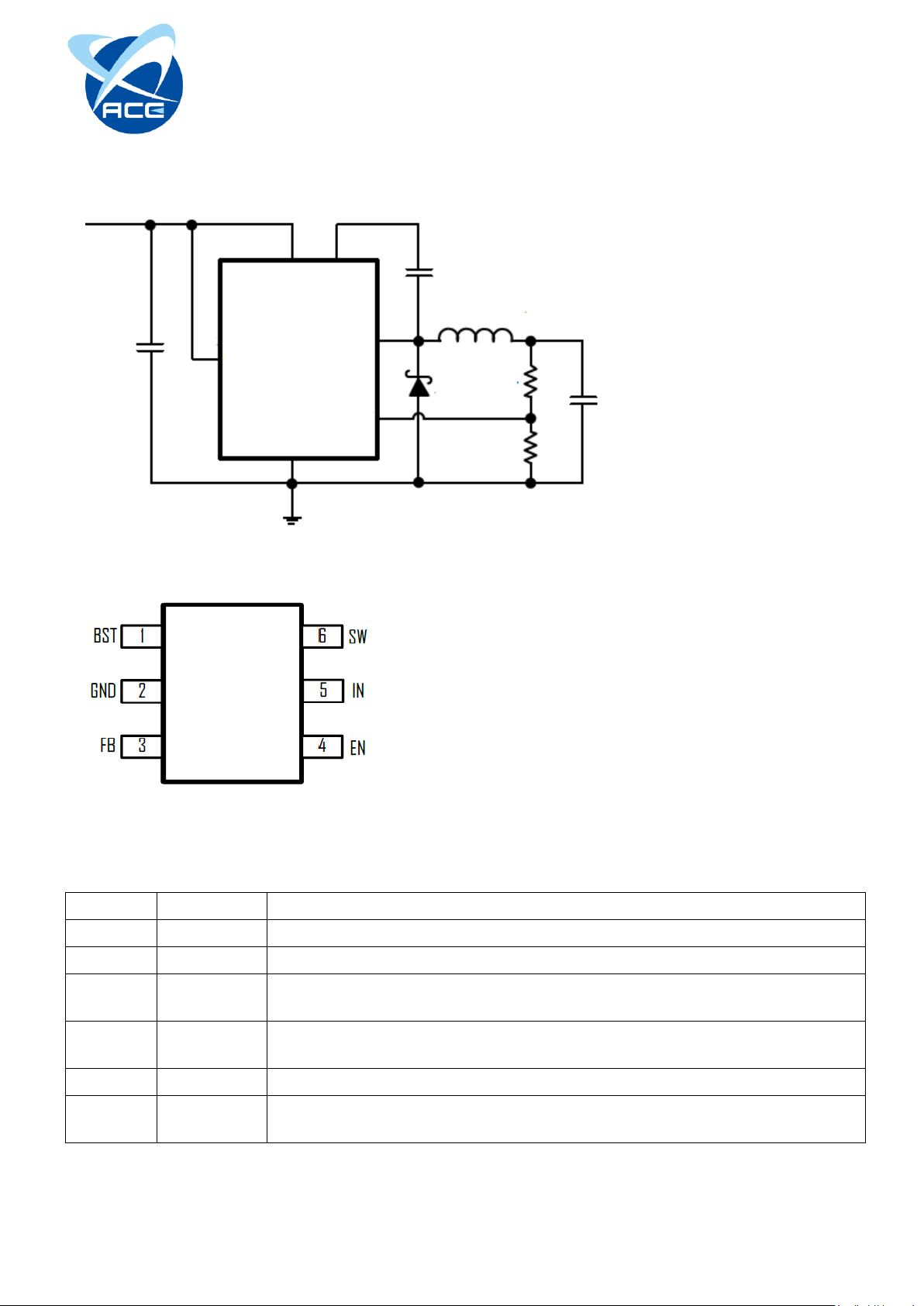
24V , 1.2A High Efficiency Step-Down Converter
SOT-23-6
Description
Function
1
BST
Bootstrap pin. Connect a 10nF capacitor from this pin to SW.
2
GND
Ground
3
FB
Feedback Input. Connect an external resistor divider from the output to
FB and GND to set V
OUT
4
EN
Enable pin for the IC. Drive this pin high to enable the part, low to
disable.
5
IN
Supply Voltage. Bypass with a 10μF ceramic capacitor to GND.
6
SW
Inductor Connection. Connect an inductor Between SW and the
regulator output.
EN
GND
B230A
3 6 49.9K
6.3V
22μF
25V
10μF
SW
FB
16.2K
2
Typical Application
VIN 12V
5 1
IN BST 10nF
V
4
Packaging Type
SOT-23-6
3.3V/1.2A
OUT
ACE725E
VER 1.1 2
Page 3
Halogen - free
GM : SOT-23-6
Pb - free
Ordering information
ACE725E XX + H
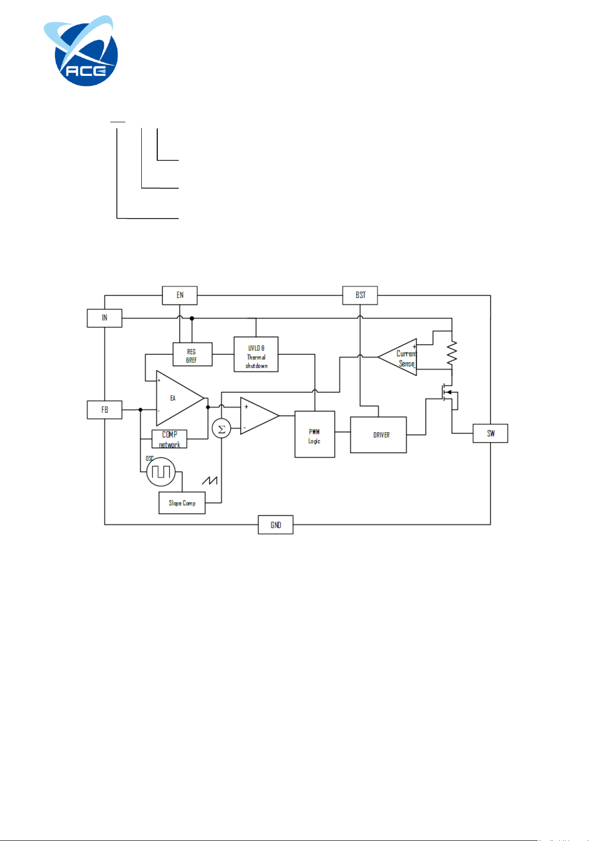
Block Diagram
ACE725E
24V , 1.2A High Efficiency Step-Down Converter
VER 1.1 3
Page 4
24V , 1.2A High Efficiency Step-Down Converter
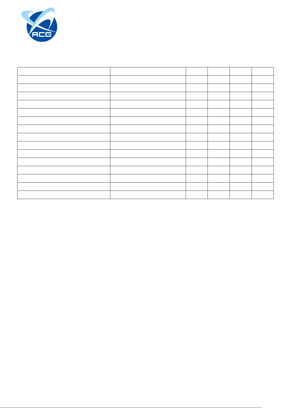
Parameter
Conditions
Min
Typ
Max
Unit
Input Voltage Range
4.2 24
V
Input UVLO
Rising, Hysteresis=140mV
3.55 V
Input OVP
Rising, Hysteresis=1.3V
26 V
Input Supply Current
VFB=0.9V
0.6 mA
Input Shutdown Current
6
uA
FB Feedback Voltage
0.79
0.81
0.83
V
FB Input Current
0.01
uA
Switching Frequency
1.0
1.4
1.8
MHz
Fold-Back Frequency
VFB=0V
100
KHz
High side Switch ON Resistance
ISW=200mA
250
500
mΩ
High side Switch Current Limit
V
IN
= 12V,
1.5 2
A
SW Leakage Current
VIN=12V, VSW=0, EN=GND
10
uA
EN Input Current
1
uA
EN Input Low Voltage
1
1.5 3 V
Thermal Shutdown
Hysteresis=40℃
150 °C
Electrical Characteristics
V
= 12V, unless otherwise specified. Typical values are at TA=25°C
IN
ACE725E
VER 1.1 4
Page 5

24V , 1.2A High Efficiency Step-Down Converter
Typical Characteristics
(Typical values are at TA=25°C unless otherwise specified)
Efficiency Vs I
OUT
I
(A) I
OUT
V
Normalized % Vs I
OUT
IOUT VOUT
I
(mA) VIN (V)
OUT
Maximum I
DUTY CYCLE (%) V
PEAK
Vs V
I
IN
Efficiency Vs I
(A)
OUT
Vs V
Vs VIN
Q
(V)
IN
ACE725E
OUT
IN
VER 1.1 5
Page 6

ACE725E
24V , 1.2A High Efficiency Step-Down Converter
Typical Characteristics
(Typical values are at TA=25°C unless otherwise specified)
V
Vs Temperature Max I
FB
Temperature(℃) Temperature(℃)
Frequency Vs Temperature Load Transient Response
Vin=12 V, VOUT=3.3V, IOUT= 0.2A to 1.0A
Temperature(℃) Ims/div
Load Transient Response Switching Waveform
Vin=12 V, VOUT=5V, IOUT= 0.2A to 1.0A Vin=12 V, VOUT=5V, IOUT= 0.5A
2ms/div 500ms/div
Vs Temperature
OUT
VER 1.1 6
Page 7

ACE725E
24V , 1.2A High Efficiency Step-Down Converter
Typical Characteristics
(Typical values are at TA=25°C unless otherwise specified)
Start-up Waveform through EN Start-up Waveform through EN
Vin=12 V, VOUT=5V, IOUT= 0A Vin=12 V, VOUT=5V, IOUT= 0.5A
5ms/div 2ms/div
Shutdown Waveform through EN Shutdown Waveform through EN
Vin=12 V, VOUT=5V, IOUT= 0A Vin=12 V, VOUT=5V, IOUT=0.5A
5ms/div 2ms/div
Short-Circuit Response Short-Circuit Recovery
Vin=12 V, VOUT=5V, IOUT=0A to Short Vin=12 V, VOUT=5V, IOUT=Short to 0A
0.5ms/div 0.5ms/div
VER 1.1 7
Page 8

ACE725E
24V , 1.2A High Efficiency Step-Down Converter
FUNCTIONAL DECRIPTIONS
Loop Operation
The ACE725E is a wide input range, high-efficiency, DC-to-DC step-down switching regulator, capable
of delivering up to 1.2A of output current, integrated with a 250m high-side MOSFET. It uses a PWM
current-mode control scheme. An error amplifier integrates error between the FB signal and the internal
reference voltage. The output of the integrator is then compared to t he sum of a current-sense signal and
the slope compensation ramp. This operation generates a PWM signal that modulates the duty cycle of
the power MOSFETs to achieve regulation for output voltage.
Light Load Operation
Traditionally, a fixed constant frequency PWM DC-DC regulator always switches even when the output
load is small. When energy is shuffling back and forth through the power MOSFETs, power is lost due to
the finite RDSONs of the MOSFETs and parasitic capacitances. At light load, this loss is prominent and
efficiency is therefore very low. ACE725E employs a proprietary control scheme that improves efficiency
in this situation by enabling the device into a power save mode during light load, thereby extending the
range of high efficiency operation.
APPLICATION INFORMATION
Setting Output Voltages
Output voltages are set by external resistors.
The FB threshold is 0.6V.
RTOP = RBOTTOM x [(VOUT / 0.6) - 1]
Inductor Selection
The peak-to-peak ripple is limited to 30% of the maximum output current. This places the peak current
far enough from the minimum overcurrent trip level to ensure reliable operation while providing enough
current ripples for the current mode converter to operate stably. In this case, for 1.2A maximum output
current, the maximum inductor ripple current is 400 mA. The inductor size is estimated as following
equation
L
=(V
IDEAL
IN(MAX)-VOUT
Therefore, for V
The inductor values is calculated to be L = 7μH.
Chose 6.8μH or 10μH
For V
OUT
=3.3V,
The inductor values is calculated to be L = 4.9μH.
Chose 4.7μH
OUT
)/I
RIPPLE*DMIN
=5V,
*(1/F
OSC
)
VER 1.1 8
Page 9

ACE725E
V
OUT
(V)
C
OUT
(μF)
L (μH)
8
22x2
10 to 15
5
22x2
6.8 to 10
3.3
22x2
4.7 to 10
2.5
22x2
3.3 to 10
FC=
2∗ π√COUT∗ L
=20Khz
24V , 1.2A High Efficiency Step-Down Converter
Output Capacitor Selection
For most applications a nominal 22μF or larger capacitor is suitable.
The ACE725E internal compensation is designed for a fixed corner frequency that is equal to
1
For example, for V
The output capacitor keeps output ripple small and ensures control-loop stability. The output capacitor
must also have low impedance at the switching frequency. Ceramic, polymer, and tantalum capacitors are
suitable, with ceramic exhibiting the lowest ESR and high-frequency impedance. Output ripple with a
ceramic output capacitor is approximately as follows:
V
RIPPLE
= IL
(PEAK)
If the capacitor has significant ESR, the output ripple component due to capacitor ESR is as follows:
V
RIPPLE(ESR)
= IL
(PEAK)
Input Capacitor Selection
The input capacitor in a DC-to-DC converter reduces current peaks drawn from the battery or other
input power source and reduces switching noise in the controller. The impedance of the input capacitor at
the switching frequency should be less than that of the input source so high-frequency switching currents
do not pass through the input source. The output capacitor keeps output ripple small and ensures
control-loop stability.
Components Selection
=5V, L=6.8μH, C
OUT
[1 / (2π x f
x ESR
OSC
x C
OUT
)]
OUT
=22μF.
VER 1.1 9
Page 10

SYMBL
MILLIMETER
MIN NOM
MAX
A 2.7 2.9 3.1 B 1.7 1.9 2.1
C -- 0.95 -- D 1.5 1.6 1.8 E 2.5 2.8 3.1 F 0.2 0.4 0.5 G 1 1.1 1.3 H 0.7 0.8 0.9 I 0 -- 0.1 J 0.2
--
--
K 0.1 0.15 0.25
Packing Information
SOT-23-6
ACE725E
24V , 1.2A High Efficiency Step-Down Converter
VER 1.1 10
Page 11

ACE725E
24V , 1.2A High Efficiency Step-Down Converter
Notes
ACE does not assume any responsibility for use as critical components in life support devices or systems
without the express written approval of the president and general counsel of ACE Electronics Co., LTD.
As sued herein:
1. Life support devices or systems are devices or systems which, (a) are intended for surgical implant
into the body, or (b) support or sustain life, and shoes failure to perform when properly used in
accordance with instructions for use provided in the labeling, can be reasonably expected to result in
a significant injury to the user.
2. A critical component is any component of a life support device or system whose failure to perform can
be reasonably expected to cause the failure of the life support device or system, or to affect its safety
or effectiveness.
ACE Technology Co., LTD.
http://www.ace-ele.com/
VER 1.1 11
Page 12

 Loading...