


ACE632
N&P Pair Enhancement Mode MOSFET
Description
The ACE632 is the N- and P-Channel enhancement mode power field effect transistors are produced
using high cell density, DMOS trench technology. This high density process is especially tailored to
minimize on-state resistance and provide superior switching performance. These devices are particularly
suited for low voltage applications such as notebook computer power management and other battery
powered circuits where high-side switching, low in-line power loss, and resistance to transients are
needed.
Features
• N-Channel
20V/0.95A,R
20V/0.75A,R
20V/0.65A,R
=380mΩ@V
DS(ON)
=450mΩ@V
DS(ON)
=800mΩ@V
DS(ON)
=4.5V
GS
=2.5V
GS
=1.8V
GS
• P-Channel
-20V/1.0A,R
-20V/0.8A,R
-20V/0.7A,R
= 520mΩ@V
DS(ON)
= 700mΩ@V
DS(ON)
= 950mΩ@V
DS(ON)
=-4.5V
GS
=-2.5V
GS
=-1.8V
GS
• Super high density cell design for extremely low RDS(ON)
• Exceptional on-resistance and maximum DC current capability
Application
• Power Management in Note book
• Portable Equipment
• Battery Powered System
• DC/DC Converter
• Load Switch
• DSC
• LCD Display inverter
VER 1.4 1
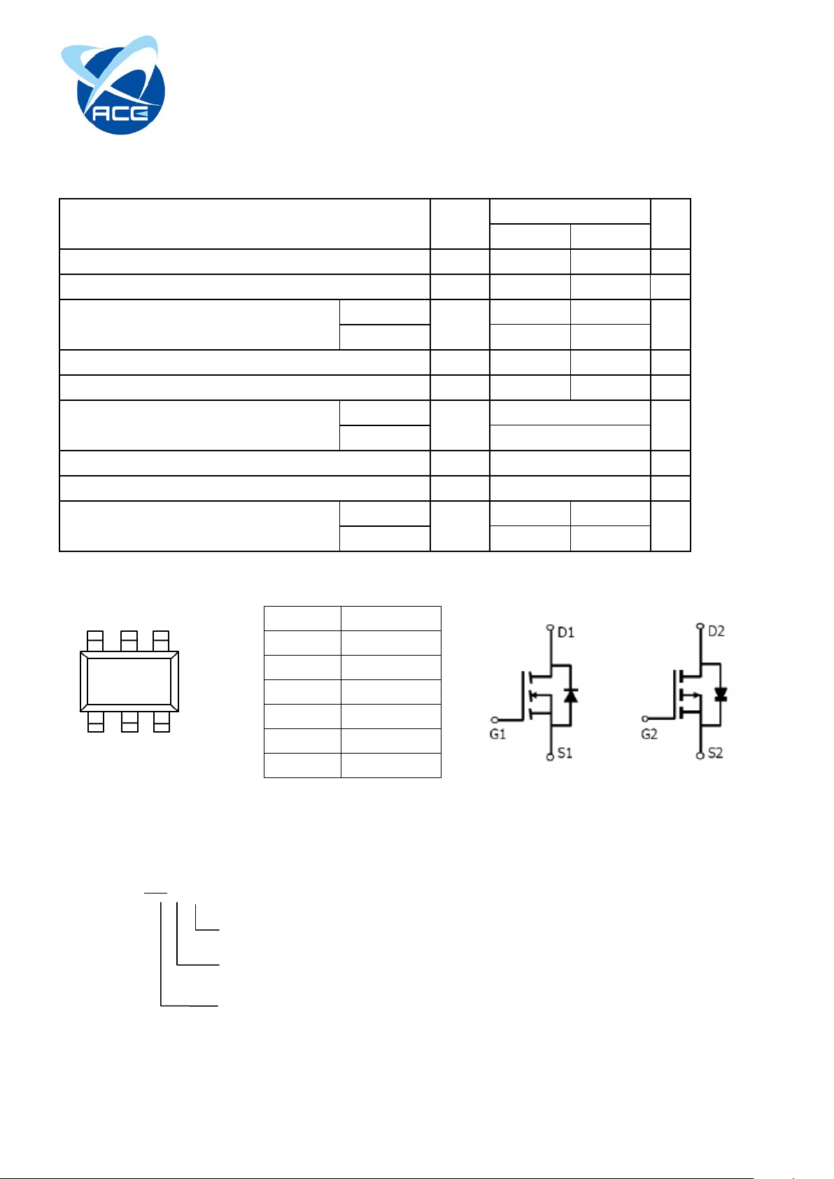
Thermal Resistance
Steady State
SOT-363
Description
1
Source 1
3
Drain 2
4
Source 2
5
Gate 2
6
Drain 1
Halogen - free
ACE632
N&P Pair Enhancement Mode MOSFET
Absolute Maximum Ratings
(TA=25℃ Unless otherwise noted)
Parameter Symbol
N-Channel P-Channel
Drain-Source Voltage VDS 20 -20 V
Gate-Source Voltage VGS ±12 ±12 V
Continuous Drain Current (TJ=150℃)
A
TA=80℃ 0.9 -0.7
I
D
=25℃
T
Pulsed Drain Current1) IDM 4 -3 A
Continuous Source Current (Diode Conduction) IS 0.6 -0.6
Power Dissipation
A
TA=70℃ 0.19
P
D
=25℃
T
Operating Junction T emperature TJ -55 to 150
Storage Temperature Range T
-55 to 150
STG
T≦10sec
-Junction to Ambient
R
θJA
Typical
1.2 -1.0
0.3
360 360
400 400
Unit
A
W
O
C
O
C
O
C/W
Packaging Type
SOT-363
6 5 4
2 Gate 1
1 2 3
N-Channel P-Channel
Ordering information
ACE632 EM + H
Pb - free
EM : SOT363
VER 1.4 2
Parameter
Symbol
Conditions
Min.
Typ.
Max.
Unit
ACE632
N&P Pair Enhancement Mode MOSFET
Electrical Characteristics
Static
V
=0V, ID=250uA N-Ch 20
Drain-Source Break do wn Voltage V
Drain-Source On Resistance R
Gate Threshold Volt age V
Gate Leakage Current I
(BR)DSS
DS(ON)
GS(th)
GSS
GS
VGS=0V, ID=250uA P-Ch -20
V
=4.5V, ID=0.95A N-Ch 0.26 0.38
GS
VGS=-4.5V, ID=-1.0A P-Ch 0.42 0.52
VGS=2.5V, ID=0.75A N-Ch 0.32 0.45
VGS=-2.5V, ID=-0.8A P-Ch 0.58 0.70
VGS=1.8V, ID=0.65A N-Ch 0.42 0.80
VGS=-1.8V, ID=-0.5A P-Ch 0.75 0.95
V
DS=VGS
, ID=250uA N-Ch 0.35 1.0
VDS=VGS, ID=-250uA P-Ch -0.35 -1.0
V
=0V, VGS=±12V N-Ch 100
DS
VDS=0V, VGS=±12V P-Ch -100
V
Ω
V
nA
Zero Gate Voltage Drain Current I
On-State Drain Current I
Diode Forward Voltage VSD
Forward Transconductance gfs
Total Gate Charge Qg
Gate-Source Charge Qgs
Gate-Drain Charge Qgd
DSS
D(ON)
V
=20V, VGS=0V N-Ch 1
DS
VDS=-20V, VGS=0V P-Ch -1
VDS=20V, VGS=0V TJ=55℃ N-Ch 5
VDS=-20V, VGS=0V TJ=55℃ P-Ch -5
V
≧4.5V, VGS =5V N-Ch 2
DS
VDS≦-4.5V, VGS =-5V P-Ch -2
I
=0.5A, VGS=0V N-Ch 0.8 1.2
S
IS=-0.5A, VGS=0V P-Ch -0.8 -1.2
V
=10V, ID=1.2A N-Ch 2.6
DS
VDS=-10V, ID=-1.0A P-Ch 1.5
Dynamic
N-Channel
V
=10V, VGS=4.5V,
DS
I
≡1.2A
D
P-Channel
V
=-10V, VGS=-4.5V,
DS
I
≡-1.0A
D
N-Ch 1.2 2.0
P-Ch 1.1 1.8
N-Ch 0.2
P-Ch 0.3
N-Ch 0.3
P-Ch 0.2
uA
A
V
S
nC
Turn-On Time
Turn-Off Time
t
d(on)
t
d(off)
tr
I
D
I
=-0.5A, V
D
tf
N-Channel
V
=10V,RL=20Ω
DD
=0.5A, V
P-Channel
V
=-10V,RL=20Ω
DD
=4.5V,RG=6Ω
GEN
=-4.5V, RG=6Ω
GEN
P-Ch 18 30
N-Ch 20 30
P-Ch 25 40
ns
N-Ch 25 40
P-Ch 20 30
N-Ch 12 20
P-Ch 12 20
VER 1.4 3
N-Ch 15 25

ACE632
N&P Pair Enhancement Mode MOSFET
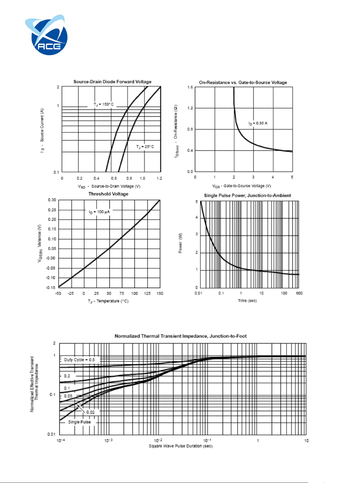
Typical Characteristics (N-Channel)
VER 1.4 4

ACE632
N&P Pair Enhancement Mode MOSFET
Typical Characteristics (N-Channel)
VER 1.4 5

ACE632
N&P Pair Enhancement Mode MOSFET
Typical Characteristics (P-Channel)
VER 1.4 6
ACE632
N&P Pair Enhancement Mode MOSFET
Typical Characteristics (P-Channel)
VER 1.4 7

ACE632
N&P Pair Enhancement Mode MOSFET
Packing Information
SOT363(SC-70-6)
VER 1.4 8

ACE632
N&P Pair Enhancement Mode MOSFET
Notes
ACE does not assume any responsibility for use as critical components in life support devices or systems
without the express written approval of the president and general counsel of ACE Electronics Co., LT D.
As sued herein:
1. Life support devices or systems are devices or systems which, (a) are intended for surgical implant
into the body, or (b) support or sustain life, and shoes failure to perform when properly used in
accordance with instructions for use provided in the labeling, can be reasonably expected to result in
a significant injury to the user.
2. A critical component is any component of a life support device or system whose failure to perform can
be reasonably expected to cause the failure of the life support device or system, o r t o affect its saf e t y
or effectiveness.
ACE Technology Co., LTD.
http://www.ace-ele.com/
VER 1.4 9

 Loading...