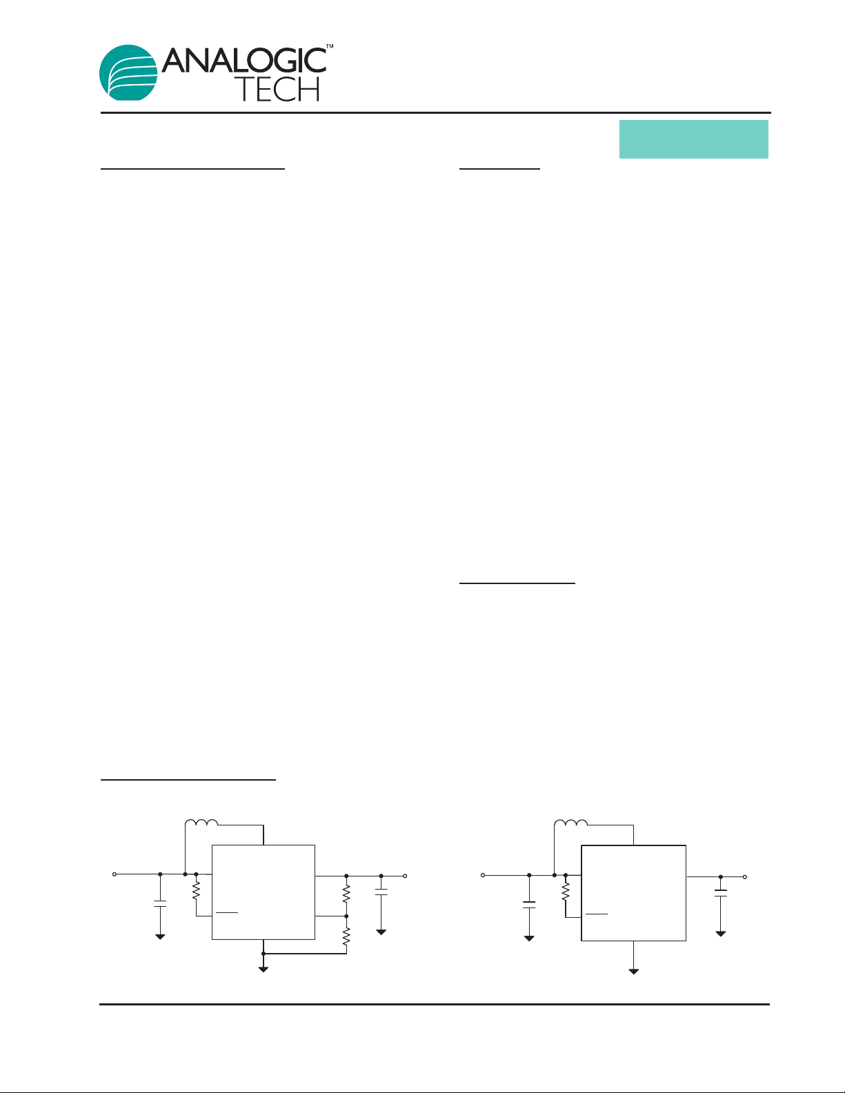
AAT AAT1217, AAT1217ICA-1.2-T1, AAT1217ICA-3.3-T1 Schematic [ru]

AAT1217
FB
VIN
SHDN
GND
VOUT
AAT1217-1.2
C
IN
4.7µF
V
IN
: 0.85 V
L1
4.7µH
R1
1.02MΩ
R2
604kΩ
V
OUT
:
3.3V,100 mA
SW
R3
1MΩ
C
OUT
4.7µF
FB
VIN
SHDN
GND
VOUT
AAT1217-3.3
C
IN
4.7µF
V
IN
:0.85V
L1
4.7µH
V
OUT
:
3.3V,100 mA
SW
R3
1MΩ
C
OUT
4.7µF
600mA, 1.2MHz, Micropower
Synchronous Step-Up Converter
General Description
The AAT1217 a high efficiency, synchronous, fixed
frequency, step-up converter designed for singlecell or dual-cell alkaline, NiMH, or NiCd batterypowered applications. The high 1.2MHz switching
frequency and completely integrated control circuitry minimize the total solution footprint area
while maintaining excellent regulation, ripple, and
transient response throughout the full load range.
Pulse skipping mode operation and low quiescent
current allow the AAT1217 to maintain high efficiency performance for light load and sleep mode
conditions. With a 1.2A peak switch current limit,
the AAT1217 is capable of delivering 100mA to the
load from a single AA cell or up to 400mA from dual
AA cells. The AAT1217 has a 0.85V start-up voltage with operation down to 0.5V.
The AAT1217 is available in a Pb-free, space-saving low profile (1mm) 6-pin TSOT23 package and
is rated over the -40°C to +85°C ambient temperature range.
SwitchReg
™
Features
•VINOperation Range: 0.5V to V
•V
Range: 2.5V to 5.5V
OUT
• 100mA Output from a Single AA Cell Input
• 400mA Output from a Dual AA Cell Input
• High Efficiency: Up to 93% Efficiency
• Low Start-Up Voltage: 0.85V Typical
• Internal Synchronous Rectifier
—V
≤ 4.5V: No External Schottky Diode
OUT
• Fixed Frequency Pulse Width Modulation
(PWM) Current-Mode Control Scheme with
Internal Compensation
• 1.2MHz Fixed Switching Frequency
• 1.2A Current Limit
• Light Load Pulse Skipping Mode Operation
• Low 80µA No Load Input Current
• Over-Current Protection
• EMI Reduction Anti-Ringing Control Circuitry
• Low Shutdown Current: <1.0µA
• -40°C to +85°C Ambient Temperature Range
• Low Profile (1mm) TSOT23-6 Package
OUT
Applications
• Cellular and Smart Phones
• Digital Still and Video Cameras
• Microprocessors and DSP Core Supplies
• MP3 Player
• Portable Instruments
• Wireless and DSL Modems
Typical Application
1217.2007.07.1.0 1

Pin Descriptions
GND
VIN
VOUT
SHDN
FB
SW
1
2
3
4
5
6
Pin # Symbol Function
1 SW Power Switch Pin. Ties to the drains of the PMOS synchronous rectifier and the
2 GND Ground Pin
3 FB Feedback Input Pin. Connect FB to the center point of the external resistor divider.
4 SHDN
5 VOUT Power Output Pin. Tied to the source of the PMOS synchronous rectifier.
6 VIN Power Supply Input. Must be closely decoupled to GND, Pin 2, with a 4.7µF or greater
Pin Configuration
AAT1217
600mA, 1.2MHz, Micropower
Synchronous Step-Up Converter
NMOS switch.
The feedback threshold voltage is 1.23V.
Shutdown Signal Input. Logic high enables the IC. Logic low disables the IC. Shutdown
current is <1µA.
ceramic capacitor.
TSOT23-6
(Top View)
2 1217.2007.07.1.0

AAT1217
600mA, 1.2MHz, Micropower
Synchronous Step-Up Converter
Absolute Maximum Ratings
1
Symbol Description Value Units
V
IN
V
SW
VFB, V
SHDN
V
OUT
T
A
T
STORAGE
T
LEAD
T
J
Thermal Information
Input Supply Voltage -0.3 to 6 V
SW Voltage -0.3 to 6 V
FB, SHDN Voltages -0.3 to 6 V
VOUT Voltage -0.3 to 6 V
Operating Ambient Temperature Range
2
-40 to 85 °C
Storage Temperature Range -65 to 150 °C
Lead Temperature (Soldering, 10s) 300 °C
Operating Junction Temperature Range
3
2
-40 to 150 °C
Symbol Description Value Units
θ
JA
P
D
Maximum Thermal Resistance 190 °C/W
Maximum Power Dissipation 526 mW
1. Absolute Maximum Ratings are those values beyond which the life of a device may be impaired.
2. TJis calculated from the ambient temperature TAand power dissipation PDaccording to the following formula: TJ= TA+ PDx θJA.
3. Mounted on an FR4 board.
1217.2007.07.1.0 3

AAT1217
600mA, 1.2MHz, Micropower
Synchronous Step-Up Converter
Electrical Characteristics
VIN= 1.2V, V
= 3.3V, TA= 25°C, unless otherwise noted.
OUT
1
Symbol Description Conditions Min Typ Max Units
Minimum Start-Up Voltage I
Minimum Operating Voltage V
Output Voltage Range 2.5 5.5 V
Output Voltage Accuracy
3
Reference Voltage TA= -40°C to +85°C 1.192 1.230 1.268 V
/ Reference Voltage Line V
Regulation VIN= 2.4V to 4.2V, I
/ Reference Voltage Load V
Regulation VIN= 3.6V, I
Quiescent Current (Shutdown) V
Quiescent Current (Active) V
V
∆V
OUT/VOUT
∆V
∆V
OUT/VOUT
∆I
V
V
IN
OUT
FB
OUT
I
Q
IN
Quiescent Current (Active) Measured on V
I
LNMOS
I
LPMOS
R
DS(ON)L
R
DS(ON)H
I
CL
NMOS Switch Leakage VSW= 5V 0.1 5 µA
PMOS Switch Leakage VSW= 0V 0.1 5 µA
NMOS Switch ON Resistance
PMOS Switch ON Resistance
NMOS Current Limit 750 1200 mA
∆t(ICL) Current Limit Delay to Output 40 ns
D
F
V
I
SHDN
T
MAX
OSC
SHDN
SD
Maximum Duty Cycle VFB= 1.15V, TA= -40°C to +85°C 80 85 %
Switching Frequency TA= -40°C to +85°C 0.9 1.2 1.5 MHz
SHDN Input Low 0.35
SHDN Input High 1.00
SHDN Input Current V
Thermal Shutdown
= 1mA 0.85 1
OUT
= V
SHDN
I
OUT
V
IN
OUT
V
OUT
V
IN
OUT
V
OUT
SHDN
IN
source. V
V
OUT
V
OUT
V
OUT
V
OUT
SHDN
IN
= 10mA; TA= -40°C to +85°C -4 +4 %
= 1.2V to 2.4V, I
OUT
= 10mA,
= 3.3V
= 10mA,
OUT
= 5.0V
= 1.2V, I
= 10mA to 100mA
OUT
= 3.3V
= 10mA to 400mA
OUT
= 5.0V
= 0 0.01 1
= 1.8V, Current from input voltage
= V
SHDN
OUT
IN
, V
SHDN
= V
IN
= 3.3V 0.35
= 5V 0.30
= 3.3V 0.60
= 5V 0.55
= 5.5V 0.01 1 µA
0.5 0.65
0.2
0.4
0.003
0.004
115 µA
300 500
160
Hysteresis 20
V
%/V
%/mA
Ω
Ω
V
°C
1. Specifications over the temperature range are guaranteed by design, characterization, and correlation with statistical process controls.
2. Not including the current into internal resistance divider.
3. For fixed 3.3V and 5.0V output voltage version. The adjustable output voltage is guaranteed by reference voltage accuracy.
4 1217.2007.07.1.0

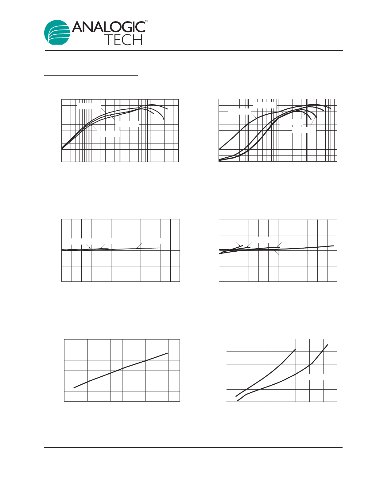
Typical Characteristics
Minimum Start-Up Voltage vs. Output Current
(V
OUT
= 3.3V; TA= 25°°C)
Output Current (mA)
Start-Up Voltage (V)
0 20 40 60 80 100 120 140 160 180 200
0.6
0.75
0.9
1.05
1.2
1.35
1.5
Maximum Output Current vs. Input Voltage
(L = 4.7µH; TA= 25°°C)
Input Voltage (V)
Maximum Output
Current (mA)
0.5 1 1.5 2 2.5 3 3.5 44.5
0
200
400
600
800
1000
V
OUT
= 5V
V
OUT
= 3.3V
Output Voltage vs. Output Current
(V
OUT
= 3.3V; TA= 25°°C)
Output Current (mA)
Output Voltage (V)
0 100 200 300 400 500 600
3.1
3.2
3.3
3.4
3.5
VIN= 1.2V
VIN= 1.5V
VIN= 2.4V
Output Voltage vs. Output Current
(V
OUT
= 5V; TA= 25°°C)
Output Current (mA)
Output Voltage (V)
0 100 200 300 400 500 600
4.8
4.9
5
5.1
5.2
VIN = 1.2V
VIN= 1.5V
VIN= 2.4V
VIN= 3.6V
Efficiency vs. Output Current
(V
O
UT
= 3.3V; TA= 25°°C)
Output Current (mA)
Efficiency (%)
0.1 1 10 100 1000
0
10
2
0
3
0
40
5
0
6
0
7
0
8
0
90
100
VIN= 2.4V
VIN= 1.2V
VIN= 1.5V
Efficiency vs. Output Current
(V
O
UT
= 5V; TA= 25°°C)
Output Current (mA)
Efficiency (%)
0.1 1 10 100 1000
0
1
0
20
30
40
50
60
70
80
9
0
1
00
VIN= 1.2V
VIN= 1.5V
VIN= 3.6V
VIN= 2.4V
AAT1217
600mA, 1.2MHz, Micropower
Synchronous Step-Up Converter
1217.2007.07.1.0 5
 Loading...