

Page 1
rry1qlicntionArFtoN
lSMHz
Application/A[RON
Dua!
oscilloscope
is
equivalent
TTM
AARON
2-2,
Nishikicho,
Chiyoda-ku,
Trace
0scilloscope
BS-3{
to
Model
CORPORATION
Kanda
Tokyo,
3O3
101
OS
Phone:
Telex:
29I-1997
222-2341
TTMTYO
Page 2
TABLE
OF CONTENTS
SECTION
SECTION
SECTION
SECTION 4 CIRCUIT DESCRIPTION
,34
I
INTRODUCTION
2
SPECIFICATIONS
3
OPERATIONS
3-l
3-2
J-J
3-5
34
3-7
3-8
3-9
3-10
3-l I
3-12
INITIAL
INTERNAL BATTERY
EXTERNAL
CONTROI.S AND INDICATIONS.
INTERNAL SWEEP AND TRIGGERING
X-Y
CALIBRATED VOLTAGE MEASUREMENTS
DUAL TRACE WAVEFORM
TV SIGNAL SYNCHRONIZATION.
ADD
BATTERY CHARGING.
APPLICATIONS
OPERATION
DC OPERATION
OPERATION.
MEASUREMENTS
SUB
&
4-1 OU"ILINESOFCIRCUIT
4-2
4-3
44
44<l) Battery Charging Circuit
44<2) Switching
.
SECTION 5
44<3) Dc-DcConverterCircuit
44-(4)
4-4-(5)
5-I
5-1-(l) Preventive Maintenance
5-1-(2)
5-l
5.2
5-2-(l) Power
5-2-(2) Vertical Amplifier Unit Adjustments
5-2<3) Horizontal/Time Base Unit Adjustments . .
VERTICAL AMPLIFIER
HORIZONTAL/TIMEBASECIRCUIT..
POWER SLIPPLY
Regulator
High
Voltage Section for CRT and Unblanking Circuit
BLOCK
MAINTENANCE AND ADJUSTMENTS
GENERAL
Cleaning
-(3)
Recalibration
ADJUSTMENTS
DIAGRAM
Supply
CIRCUIT
AND CALIBRATION
Unit
(AC
Power
OPERATION
OBSERVATION
CIRCUIT
Circuit
Adjustments
Line).
. .
.....hgEI
3
3
1
1
7
7
7
7
7
8
8
t
.......
13
13
.......t4
t{
l.f
.....--
.
.
t.f
15
15
t5
l6
t6
I6
l5
l5
rt
n
SECTION
SECTION
PARTS LIST
6
6-I CHASSIS.
6.2 VERTICAL
6.3
64
HORIZONTAL/TIME
POWER
AMPLIFIER UNIT. .
SUPPLY
UNIT.
7 SERVICING
7-I CIRCUIT
7-l-(l) Components
7.2 CIRCUIT
-2-(l)
7
Components
DIAGRAM
Location Diagram
DIAGRAM
Location
7.3 CIRCUIT DIAGRAM
-3-(l)
7
Components
l,ocation
BASE UNIT
FOR VERTICAL
FOR HORIZONTAL/TIME
Diagram
FOR POWER
Diagram
AMPLIFIER
SIJPPLY
I.]NIT.
I.]NIT
BASE
IJNIT .
2t
23
24
26
28
D
30
3l
32
l_r
Page 3
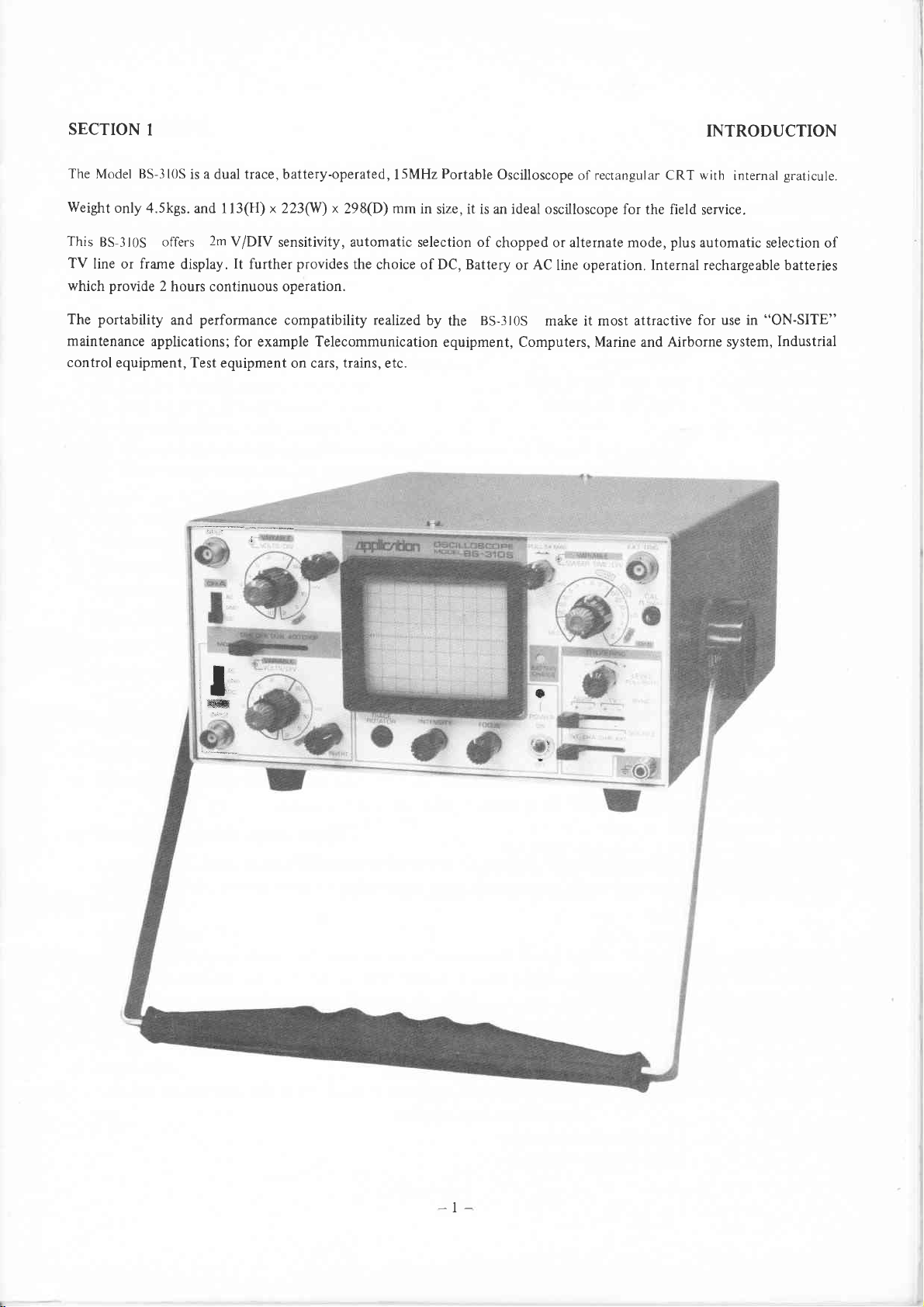
SECTION
I
INTRODUCTION
The
Weight
This
TV
which provide
The
maintenance
control
BS-3t0Sisadual
Model
only
4.5kgs. and 1
BS-310S
line or frame
portability
equipment, Test equipment
trace,battery-operated,
x 2B(fD x
l3(H)
offers
2
applications;
2m
V/DIV
display.
hours continuous operation.
performance
and
sensitivity, automatic selection of
It
further
compatibility realized
for example Telecommunication
on cars,
,I
provides
l5MHzPortableOscilloscopeof
298(D)
mm
in
the
choice of DC, Battery
by
trains,
etc.
rectangular CRTwith
size, it is an ideal oscilloscope
chopped or alternate mode,
or AC
line operation.
BS-310S
the
equipment, Computers,
make it most attractive
Marine
for the field
plus
Internal
Airborne system,
and
internal
service.
automatic
rechargeable batteries
for use in
graticule.
selection of
"ON-SITE"
Industrial
,I'
rry
*
!
-1-
Page 4

SECTION 2
VERTICAL DEFLECTION
Deflection Factor
2mV to
Bandwidth DC:
AC:
10V
DC to
l0Hz
to
Risetime 24nw,
Overshot Less than
lnput Impedance
Operating Modes CH-A, CH-B,
Chop
Frequency 200KHz approx.
Channel Separation
CH-B
Polality
TIMB BASE
Type
Sweep
Time 0.5p sec to
lMp
Better
CH-B
Automatic
Magnifier x5 at all
Linearity Less
TRICCERING
Sensitivity INT:
EXT:
Source
Slope
Range
TV Sync
INT,
Positive
20Hz to
Vertical and
be synchronized
TV-H(Line)andTV-V
TV-V: 0.5sec
TV-H:
3%
shunted
60dB
than
can be inverted
and
0.5sec/ DIV
ranges
than 3%
I
DIY or
I
Vp-p
CH-A, CH-B'
and Negative,
l5MHz
Horizontal Sync
50,12 sec/
DIY on
/
l5MHz(-3dB)
l5MHz(-3dB)
dy
12 ranges
20pE+3pF
DUAL, ADD and CHOP
at lkHz.
triggered.
more
and expanded for
DIY to 0.lmsec/ DIV.
/
DIV to 0.5p
In automatic mode, sweep is
19 ranges in l-2-5 step
on
or EXT
continuously
separator
(Frame)sync
are switched
sec/
in
variable
viewing.
DIV.
step with
l-2-5
level: Pull for AUTO
circuitry allows any
automatically by SWEEP
hne control.
obtained
with
without input signal.
fine control and X-Y.
portionof
SPECIFICATIONS
complex
TVvideo waveform to
TIME
DIV switch.
/
HORIZONTAL DBFLECTION
Dellection Factor 2mVto
Frequency
Input Impedance lMg shunted by
Max Input
X-Y
Response
Voltage
Operation
DC to
300V DC+AC
X-Y
CH-A:
CH-B:
OTHER
SPECIFICATIONS
CRT 95mm
Calibration Voltage
Power Requirements
0.5Yp-pr+ 5%,
AC: 90-
l0Y/
OIV on
lMHz
mode is selected by SWEEP TI]I{E
Y axis
X axis
tube(approx.
lKHz
l30Y
DC:11-30Y;7.2Y4
Weight
Battery:
Charging
4.5kgs(5.5kgs including
I 13(H) x 223(W)
Ni-Cad
Time:
l6hours (While
12 ranges
20pF+3pF
peak
or 600Vp-P
l.5KY)
Squre Wave.
180-260V;
or
Battery(up
6hours(Scope
battery)
x 298(D)mm
in
l-2-5
48-440H2
2 hour
to
not operated)
Scope operated)
-2-
step with fine control.
DIV switch
/
operation)
Page 5
SECTION 3
INITIAL
3-I
OPERATION
OPERATION
Inspect
inspect
the
the instrument itself.
carton
for
serious
INITIAL AC OPERATION
Prior
1.
2.
3.
4. Adjust
5. Readjust Vertical
to any kind of
a) Set the
b) Turn
Turn INTENSITY
c)
Push
d)
PuIl
e)
The rest
0
g)
Check
Connect the AC
POWER
all the three
PULL
the
TRIGGERING LEVEL
of the controls
the line
outlet. Then the
Ni-Cd
battery.
POWER
Turn
INTENSITY
FOCUS
(Power
to ON. After approximately
clockwise
and
operation
5X MAG
voltage.
line cable into
LED
INTENSITY
and
damage which might
If damage
of the instrument,
to OFF.
switch
POSITION
control
controls
to mid-position.
control
control
remain at any
the
BATTERY
source; AC
till trace lines
controls
Horizontal
POSITION
have
the agent
for
notify
to
mid-position.
normal.
proceed
is noted,
for AUTO.
position.
AC receptacle
CHARGE indicator
(or
EXT
are easily observed.
position)
DC)
20 seconds, trace lines appear on
for
clear trace lines.
controls
the failure of the
caused
you
follolvs to
as
on the rear
is lit up in
for
locations
instrument
bought from
get
panel
red, which means
required.
before making any operation.
familiarized with
of the instrument, and
CRT
transportation.
during
the
instrument.
plug
that the set is charging
If
trace lines
screen.
no
an
into
the
appear, rotate
AC
internal
And
power
Connect
6.
Rotate CH-A Vertical
7.
wise to detent. Turn TRIGGERING
8. Readjust INTENSITY, FOCUS for
RemoveprobetipfromCAL0.5Vp-poutput.Now,theoscilloscopeisreadyforobservationofwaveforms.
9.
probe (10:1)
a
INPUT of CH-A and hook the tip of the
to
attenuator
VOLTS/DIV
SOURCE to CH-A.
clearer
switch to l0mV/DIV
display.
Then
probe
and
a
square-wave
to CAL
turn the
of
0.5Vp-p
output.
VARIABLE on the same
5 divisions is
3.2 INTERNAL BATTERY OPERATION
It
1.
required to
is
ment
is not in
battery.
2.
RECHARGING
Connect
gins
whether POWER switch
ON,
color
(or
EXT DC)position)
use. Whereas, while the instrument is in use,
the AC
takes
l6
it
lrom red to
charge
power
hours
green.
up
internal
cable to
for full
Then
battery
AC outlet
is ON or
recovery.
automatically trickle
to lull before
and to
OFF. When it is turned
Whenever the
operation.
the recharging
It takes only 6
AC receptacle of the
to OFF,
battery is charged,
charging starts
to
takes
oscilloscope.
recharging
BATTERY
maintain the
hours to
hours
16
Then
lull charged
recharge while
to reach the
recharging
requires
CHARGE
3. OPERATION
Turn
tion.
POWER
SOURCE
slide switch
found
on rear
panel
BATTERY
to
(INT),
and operate
the same
displayed on
full
automatically
hours,
6
only
indicator
level.(Power
way as AC opera-
axis
clock-
the
screen.
the
instru-
of the
level
andwhen
changes
source;
he-
its
AC
-3-
Page 6
SECTION 3 OPERATION
EXTERNAL
3.3
Make
sure
type of I lV up
in-between
34
CONTROLS
I.
VERTICAL
Vertical input
2,
AC.GND.
Vertical input couplingfor
position,
rectly
connected
3.
MODE
DC OPERATION
EXT
the
to 30V,
would
not ill-effect
& INDICATIONS
INPUT
terminal
DC
the input
DC
to the
CH-A: Waveforms
CH-B:
DUAL:
ADD
CHOP:
4.
VOLTS
5. VOLTS
Vertical attenuator
Calibrated voltage
to
6. VERTICAL
Vertical
7.
HORIZONTAL
Horizontal
8. SWEEP
Horizontal
operation is
Change
9.
SWEEP TIME
IO.
EXT.
Waveforms of CH-B are displayed
In
range from 0.5sec/ DIV
the
In
range from 0.5msec
the
: CH-A and
This is chop
DrV VARTABLE
/
DrV
/
input'voltage
the
POSITION
position
position
TrME
/
sweeptime selector. It selects sweeptimes
possible
over between CHOPand
/
TRIG
Input for external
1I.
CAL
Calibration voltage
12. BATTERY
Indicates
When
I3.
TRIGGERING
LEVEL control
CHARGE
the charging and charged.
battery is chaged enough for
adjusts
PULL AUTO
pulling
By
signal
With
is set in free-running
LEVEL knob
is applied, with
trigger signal, triggered-sweep
INPUT
receptacle
withstanding
the
operation of
is correctly wired to
the
current
drain
the
for CH-A.
CH-A. In AC
terminal
of CH-A
opens and
amplifier and all components
are
displayed.
/
CH-B signals are
mode all
cinly
for CH-A. The scale is
is indicated when VAR,IABLE
used. Selectableinl2 calibratedranges
adjDster for
POSITION
adj uster.
DrV
by
DrV
triggering signal.
terminal. Calibration voltage
LEVEL
state.
CH-A.
turning the
knob
ALTERNATEis
VARIABLE
use this lamp
phase
sync
toward
line displayed on CRT.
trace
to
you,
is effectedwhere
position,
input
the
up
to
DIV up
added.
throughthe
graduated
fully clockwise
determine
auto-sweep
of internal amplifier is
lmsec
to 0.5p sec
sweepranges.
is
changes from red
the starting
polarities (+
its
of 7 .2YA.
instrument.
the DC componetof input signal is blocked
of input signal are
DlY, both channels
/
in voltage
is turned fullyclockwise.
The
The
DIV, both
/
per
wide
EXT
"DIV"
from 2mY
of 0.5p sec/ DIV
CH-B.
to
also accomplished
0.5Vp-p of about lKHz
is
effected;
sync
level is
automatically by
green.
to
point
of sw@p on the slope
the sweep is
adjustable. Whensync level
&
-).
voltage variation
DC
source
grounded.
displayed.
are
channels are
CRT
of
Set this cnotrol for
DIY
to
/
to0.5sec
/
square wave.
set in free-running
DC external
The
will not charge
position,
In DC
chopped at about
switched alternately..
screen
10V
DlV.
/
DIY in 19 calibratedsteps.
this selector in DUAL
of
be any
could
source
range means the fluctuations
the internal battery.
the
area.
proper
by capacitor.
input
l00KHz.
waveform according
InGND
terminal is di-
X-Y
MQDE.
displayed
waveform.
state even when
deviated,
is
no input
sweep
the
Page 7
I
SECTION 3
OPERATION
14.
POWER ON LAMP
I5.
SYNC
Sync
sweep is started
I6.
SOURCE
Sync source
polarity
selector.
signal selector switch;
At
with negative slope.
INT : Mixed signal of
:
CH-A
CH-B
EXT
11.
GROUNDED
18
POWER SWITCH
Turns
ed off.
FOCUS
19.
Focus control to obtain
INTENSITY
20
Adjust the brightness ol waveform
TRACE ROTATOR
21.
The earth magnetics effect the
22
PULL INVERT
When
CH-A vertical input
:
CH-B vertical input signal
:
The signal applied to
TERMINAL
power
on or off.
optimum
pulled,
CH-B
is inverted,
" position
"
the
t
and CH-B
CH-A
signal is used
EXT TRIG is used
power
AC
waveform
for easy
trace
and
FRONT
VIEW
of rhe switch. sweep
becomes
is used
connected,normal chargingBwhile
line
display.
line Rotate this
accomodates ADD ro SUB
this
as sync
as sync
viewtng.
sync source
signal.
signal
as
sync signal
with a screw driver
is started with
switch is
this
proper
for
mode.
positive
trace
the
"
at
slope;
onandquickchargingwhenturn-
line
position,
"
the
-5-
Page 8
SECTION
3
OPERATION
.!.)
voLTS
Same
VOLTS
Same
25
VERTICAL INPUT
Same
26
AC-GND-DC
Same
POWER
AC(or EXT
BATTERY(INT):
AC POWER
28
90V-130V
29, EXT
With use of
is inserted,
same
BATTERY COMPARTMENT
30.
Remove
olf the
DrV
/
as
for CH-B
5.
DIV
/
4. lor CH-B
as
1. for CH-B
as
2. for CH-B
as
SOURCE
AC or
DC
Priority
level.
right-side rwo
the
connector
VARIABLE
DC):
Internal
LINE
EXT
ol
AC operation
battery
RECEPTACLE
l80V-260V
AC,
DC INPUT
given
is
battery
to
legs on
before taking
DC operationfrom
and
operation.
40Hz to440Hz
receptacle,
DC
EXT
panel
rear
out
REAR
connect
source even
battery.
llv
and take
Installation
VIEW
1lV
to30V
DC source
30V
to
other sources
off the
four screws
battery should
of
DC
for operation.
are connected.
for
opening
be done
Power
BATT
vice versa.
Whenthe
consumptionis
External
COMPARTMENT.
plug
DC
maintainedthe
Pull
-6-
Page 9
SECTION 3
OPERATION
INTERNAL
3.5
TRIGGERING
L
PULLAUTO
In
2.
3. Set
4.
5.. For
the
the
trace at
of TRIGGERING LEVEL
SYNC
display waveform or
waveform.
Most waveforms can
triggering
normal
a waveform
S}ryEEP
provides
presence
which
switch
source
operation the magnifing switch,
desired,
is
by a factor of 5.
Set
6.
NOTE']
TIME/DIV
sweep
USING THE 5X MAG
WHICH CAUSES LESS
X-Y
3-6
For
to CH-B.
OPERATION
some special cases,
Then
all CH-B
TRIGGERING
AND
LEVEL knob
automatic
of
input signal
triggering
sweep
control
NORM(+)
to
(-)
to the
be observed
is required,
this instrument is specially
functions work
turn to
pull
5X
and VARIABLE
switch
POSITION, THE
either
selects
recurrent sweep
for triggering, no
occurs is selected
is to obtain a stable
position
position
by using
EXT
MAG
ELECTRON TO
as horizontal
AUTO lor automatic recurrent sweep
found
is
of
in the absence
difference
by adjusting
waveform display.
the
if
if the sweep is to
INT,
apply the triggering signal
and
5X MAG
out.
switch
control
is to be triggered
sweep
be triggered
CH-A, CH-B
pushed-in to operate without
is
That will
expand
for the desired number
as internal
TRACE LINE BECOMES
EMIT
LIGHT
designed for easy
amplifier,
FROM THE
X-Y application.
whereas
for triggering.
signal
input
between
AUTO and normal
TRIGGERING
point
a
at
point
at a
TRIGGERING
EXT
to
the
CH-A
and waveform
sweep
of
DIMMER
PHOSPHOR LAYER ON
remains as
or nonnal
LEVEL control.
positive
the
on
the negative
on
SOURCE.
TRIG input.
magnification.
wave
cycles
BECAUSE
Simply
turn SWEEP
vertical
triggering sweep
modes.
The
The main
goingportion
going portion
When an external
If magnification
to be observed
displayed.
to be
OF INCREASED
THE
TIME/DIV
amplifier.
operation.
point
on
purpose
of the
of the
horizontally
SWEEP
FACE.
CRT
switch
of
3-7 CALIBRATED
Peak
voltages,
this
using
inputs.
1. Set
proper
For DC or
2.
reference level. Set
wards; a negative
tion
INoTE-l
3-8 DUAL
MODE
peak-to-peak
instrument
Proceed
as
VARIABLE
to be observed.
size
complex signals, set
(by
division) by
WHEN A
MEASURED.
TRACE WAVEFORM
to be
switch
VOLTAGE
as a voltmeter.
follows;
control
voltage
PROBE
turned to
MEASUREMENTS
voltages,
fully
Vertical
the
switch
will deflect the
the
setting
(r0:l)
DUAL. Other
Voltages can
clockwise
to DC and observe
of the
rS
OBSERVATION
3.9 TV SIGNAL SYNCHRONIZATION
Set TRIGGERINC
and line
signal.
TV frame
SYNC to TV
and line
(+
or
waveform
DC voltages and
POSITION
the input switch
voltages
be measured
position,
CAL
to
controls may be
to
the amount of
trace downward. To calculate
VOLTS/DIV
USED, THE WAVEFORM DTSPLAY
procedures
then
-),
specially
easily obtained by simply
are
switch.
are
designed circuitry
GND,
the
in
a
of
specific
whenever
then
turned
adjust
and
same
waveforms are observed
set
deflection.
manners
portion
of
a
contplex
VOLTS/DIV control
to
obtain
the vertical
the voltage
IS
ONLY
as mentioned
provides
SWEEP
tuning
division
positive
A
easy
reference.
POSITION
reading, multiply
ri 10 OF
triggering
TIME/DIV
waveform can
using either
display
to
control
voltage
will deflect
the
THE ACTUAL
above.
lor
complexed
control.
be measured
or CH-B
CH-A
the waveform in
to a
convenient
trace up-
vertical deflec-
VOLTACE
frame
TV
-7 -
Page 10
SECTION
3-10
ADD & SUB MEASI.REMENTS
Sinply
Withthis
Polarity
}11
3
turn MODE switch to
MODE
at
ADD
of CH-B.
BATTERY CHARGING
ADD, added waveform
position,
subtracted waveform is
ol CH-A
and CH-B is displayed.
pulling
obtained
by
OPERATION
PULL INVERT knob whichinvertsthe
The
Charging circuit in the
The
internal
l When the
TERY
matically
If
2.
this
3. Whenever
NoTEI
3-12 APPLICATIONS
This
various effective measurements
[srNclp-rn
Either
charging circuit
instrument is switched
CHARGE
changed
the instrument
takes 6 hours.
case
the internal battery
EXTERNAL
THE
is a dual trace
Channel
controls:
Set
A
indicator changes
to trickle
is switched
oscilloscope
ACE APPLICATIoNS]
Channel
or
AC.GND.DC.
MODE
SYNC
SOURCE
PROBE
power
supply section operates
works in two
to maintain the full
off,
is charged up
DC SOURCE
feasible.
are
B
ways.
the
on,
which has full
canbe usedfor single-trace operation.
normal charge circuit charges
from red to
the
internal
WILL
green
charged level.
quick
to full,
charging changes
NOT
CHARGE THE INTERNAL BATTERY.
capability of
AC
CH-A
NORM+
INT or
to CH-A
(l
from either 90V to 130V or 180V
the battery with l/10C.
when the
charge charges
battery
Recharge
is
requires l6
the
battery
fully
charged,
with approx. ll4C and
to trickle from either
mode.
single trace
Channel
CH-A
Thanks
Ais referredtohereunder
INPUT Jack
: l)
to 260V
The
and normal charging is
hours.
quick or normal charge.
the dualtrace functions,
to
normalACpower.
frontpanelBAT-
auto-
lull recharge in
for
Connect the
chassis or the
tip
ground part.
@\UrIION!!T]
of the
probe
THE
EXCEED 600
poi
nt
the
to
PEAK-TO-PEAK
VOLTS.
in
circuit where the wave
the
form is
VOLTAGE AT THE POINT OF
-8-
measured, and
be
to
MEASUREMENT
ground
its
SHOULD
clip
NOT
to the
Page 11

SECTION
3
OPERATION
3.I2.( I)AC
When
measuring
their calibrated
@at
(EX)
The
(a)
Peak voltage
(b)
p-p
voltage
(c)
Effective
(d)
Fre4uency (Hz)
Therefore,
VOLTAGE
voltage
detent
signal displayed
\
or,,
l--
.
.
voltage.
.
the Fig I
:
is
AND FREQI.,IENCY
and frequency,
points (clockwise).
on the
set VOLTS
CRT is : Fig. I
--]
2Y
DIV x2
/
2Y
DIY
/
Peak voltage
I
**
DIV:
x4
DIV:
=2:4(V)x
Time
/
Time:Number
MEAST,RENIENT
DIV
/
\
--r
Fig.
4 volts
8 volts
:
2.828
(second)
value
VARIABLEs
4Drv
1
2
volts
of
DIVs
of SWEEP
(b)
for I
@,
cycle
TIME
and SWEEP TLME
@
VOLT
SWEEP
DIV......
/
TIME
x
DIV
/
at 2V
DIV...... at
/
DIV VARIABLE
/
5msec
Frequency:
3.12.(21DC
AC-GND-DC
set
the switchto
place
as
volt
O
After
that,
turn the switch
DC
voltage
When
the
trace line
5msec
50 Hz
The
attenuation,
10.
by
VOLTAGE
being
at AC
GND and
reference.
:
Shilt
shifts
(DIV)
X
4
input of
pull
this oscilloscope
the irnpedance
MEASUREMENT
position,
only AC or AC
TRIGGERING
the
to DC. Then
(DIV)
up-ward,
x
the
VOLTS
polarity
20m
sec
becomes lOM
the trace line
DIV
/
(
is
f
is lMg
component
LEVEL
shifts
and
),
-9
shunted by 20pF
shunted
O
knob@for
up
or down.
down-ward
was
by l5pF.
displayed
atrace
The value
(
is
capacitance.
Then
line,
-).
Whenthe
the voltage reading
on
the CRT screen.
which must
of movement
probe
is
must
be multiplied
For DC
positioned
be
is
the DC voltage.
Measurement,
usedin l0: 1
at a@rtain
Page 12

SECTION
3
OPERATION
3.12.(3),dM MODI.LATION
There are
when
3.12-1
MODE switch
Then,
3-I2-(5)
(EX)
various
carrier
the
4I
DUAL.TRACE
comparison
LB\tsL COMPARISON
OUTPUT
ways of
frequency
beingturnedto
of two
INPUT
/
measurements,
withinthe
is
APPLICATIONS
relative
an
of
MEASLREMENT
herein
but
frequency
Fig.2
Channel
signals
amPlifier
both
are
easily
DUAL,
manual
this
bandwidth
A and
compared
of
_1
I
the
B
such
Channel
envelope
the
oscilloscope.
B
as 1evel,
waveforms,
methodis
See Fig. 2
Mod.
works
introduced'This
(%):
AB
A+ts
-)
simultaneously.
phase,
etc.
method
100
is applicable
With the
place
of the
If the
connections
CH-B
amplifier.
two signals
amptifier.
viewing only
waveform
do not
simply turn
Then,
distortion.
Fig.
the
of
CH-B).
onto
match
rhe
When thereis
Set the
3,
each other
MODE
displays
Thenthe
even
switch
nodistortion originated
of
difference
variable
ADD
to
OUTPUT
3
Fig.
putl
in
CH-B
adjusted,
are
the
amplifier,
the
CH-A and
betweenredings
controls
and
same
the
of CH-A
the difference
position
CH-B
a straighttrace
t
(POSITION
VOLTS
knod
/
is the
for
line is
zaTa-j
controls
and CH-B's
DIY
distortion
invert
displayedinSUB
could be
(SUB
adjusted
is
the
caused in the
MODE),
MODE
to
gain
for
-
l0-
Page 13

SECTION
3
OPERATION
3.12.{.6l.
Every stereo equipment has
So,
}rz-l7lTv
Triggered
(line)
SYNC
}12.(8I
The most
and sync
pul
REPAIRING STEREO SYSTEMS
two
simultaneous comparison of the same
SERVTCTNG
oscilloscope is indispensable.
for accurate
PULSES.
COMPOSITE
important waveform
pulses.
ses.
synchronization to
VIDEO ANALYSIS
4
Fig
and Fig.
symmetrical amplifier
stages
This model
view VIDEO
circuits.
it so easy
makes
has the very convenient TV
SIGNAL, BLANKING PEDESTALS,
in TV servicing is the composite
5 shows composite signals
VIDEO
synchronized with
Fig.4
to locate
signal
defective
consisting
horizontal
Fig. 5
point.
SYNC
of the
circuits
video signal,
sync
TV-V(Frame) and TV-H
of
and Vertical
VITS
pulses
Horizontal
/
blanking
the
and vertical blanking
pedestals,
HORI
SYNC
AL
PULSE BLANKING
PULSE
-
ll
VERTICAL
SYNC
PULSE
VERTICAI.
BLANKINi
-
Page 14

SECTION 3
OPERATION
3.12.19]'
Simply turn SWEEP TIME
Connect a standard
screen as shown
MEASI.]REMENT
frequency signal to
in Fig
6.
Standard signal
((8
/ros,
3.12.(10)
In X-Y
PHASE
function,
MEAST.,REMENT
apply
OF
DIV
/
frequency:
))
twosignalsi
FREQUENCY
switch to
CH-B
CH-B and
Unknown
1
I
-:
2
l:1
each CH-A
to
BY X.Y
for X-Y
unknown
signal
and CH-B.
operation.
signal to
frequency
Calculate according
Then CH-A
CH-A.
becomes Y axis
Lissajous' figure
formula.
to the
and CH-B
is displayed on the
I
I
1-
2
6l
X
axis.
slNE
-12-
/:R
6:
PHASE
Page 15

SECTION 4
Fig.6 shows
of this Manual.
the
BLOCK DIAGRAM
of the oscilloscope.
The
circuit
is
shown
in
the
circuit
CIRCUTT
diagram
DESCRIPTION
given
at the
SECTION
7
4.I OUTLINES
This oscilloscope
to the
required level, amplified
trigger
signal. The
over
between CH-A
In
DUAL-TRACE operation, CHOP
switch.
of CRT.
that
the
This
is always being recharged
with
which
each
feedback-type
4-2
The
attenuator,
DUAL
then applied
makes
9, 10), the
made of
The
input
At
the same time the trigger signal
drive the
pulse
clock
oscilloscope is operated
the
Switching
controls
section
as the
VERTICAL
vertical input
where
FET
through high input impedance.
to the 2nd
the
selection
output
Q7,8,31,32.
CIRCUIT
OF
provided
is
switching circuit consists of
and CH-B, or
proper
after
saw-tooth
applied to the horizontal
is
the
constant
generating
whenever a line cord
Regulator.
pulse
width to supply constant
power
source.
voltage
AMPLIFIER CIRCUIT
fed from the
signal
1/10 step
attenuator composed
of lll,l/2.5,1/5 steps.
is fed to the diode
signal
two
with
pre-amplifier,
the
at
DUAL
(at
switching
circuit
by the
three different
Highly
stable
The high voltage
circuit.
BNC input terminal
(20d8)
attenuation
identical
as
input attenuators and
and
diode
circuit
well
as trigger signals.
200KHz)
fed
is
and ALTERNATE
to the
out of mode
after being
deflection
and elficient operation is made
plate
power
is
connected.
to the
led
and mode control
output amplifier and
control
amplified at the
CRT, after being
of
source;
All voltages
output level, free
for
CRTisalsobeingsupplied,afterbeingfurtherstablizedthroughthe
is controlled
place.
DUAL
takes
FET
The
is well DC balanced
two vertical
switching
are automatically selected
logic circuit,
trigger amplifier.
EXT
AC,
are
from fluctuations.
by the
of input
out
ol lCl(lC2). The 2nd attenuator composed
modilying
switching
gain
ICI(IC2).
of
circuit composed
Alter being
of
pre-amplifiers.
part
circuit,
is finally
amplified.
DC and Battery.
supplied
possible
a
logic
circuit,
the external
or
AC-GND-DC
which accomplishes
applied to the
The
to the DC to DC converter
the use of this Switching
by
The
protection
against temperature
of
DC
balanced,
D2-5,
l6-19
as
The input is
the
of
signal
SWEEP
by
vertical deflection
will be clock
source,
saw-tooth
AC operation, the
In
converter
switch
circuit
ICI(lC2).
well as
output is
and applied
Ql(Q25)
variation.
The 2nd attenuator
through
to the trigger
attenuated
being
separated
the
change-
TIMEiDIV
generated
wave
Battery
connected
Regulator
supplied
to the
fed to
is
The output
VR1,3,4(VR7,
amplifier
as
plate
pulses
by
to
lst
the
is
The mode logic circuit
possible.
ALT
vertical MODE
In X-Y operation,
the horizontal
The vertical signal
and then
level,
Dual-trace operation is obtained
switch works
controlled
amplifier as the
through diode switching
fed to the output
is
feedbacktype amplifier
(Q21,22)
of CRT.
for
high frequency corrtents
which
is controlled
prior to TRIG SOURCE
SWEEP
by the
X
signal.
amplifier
the
with
constant
to obtain
by the
MODE
by the
trigger
switch and selects
TIME/DIV
passes
circuit
composed of
current circuit
flat response
switch, makesthe
logic
select
control,
-
CH-B signal
the limiter circuit
Q15-24.
(Q19,
13
The output obtained is sufficiently
20,23,24).
signals.
The signal is
-
selectionof
driven by TRIG
circuit
proper
a
supplied
is
of
Qll,
This amplifier is
dual-trace,single-trace,CHOPand
SOURCE switch,
trigger signal
l2 and
then fed to
for single-trace
to the trigger
D6-9 to obtain
equipped
vertical deflection
the
amplifier
amplified
with the booster
the
while
operation.
and fed
the adequate
the
by
plates
to
Page 16

SECTION
4
CIRCUIT
DESCRIPTION
4.3 HORIZONTAL/TIME BASE
Base
Time
trigger
select
the
and
trigger
rJirectly
horiz.ontal sync signal
and TVV is autor.natically
into
(Q10.
gate
high level
inverted.
SWEEP
saw-tooth
signal
fed
square
IC4c. d).
automatic
starrs
and the
and
TIME/DIV switch
fully rises. the
Hold-off
the
The output
consists
circuit
circuit is led
wave
being amplified
is
ICl. With TRIG SOURCE switch set
to
waves and becomes clock
With
gate F.F.
sets
Q4
Hold-off F.F.
passes.
time
ol this
Miller
ln this arnplifier. by
X-Y position.
switch set
f ier and then the
to
vertical Ctl-B
of trigger
to
sweep
antplifier
(TVH)
or vertical
acconrplisheci
trigger
no
sweeping.
is inverted
to OFF, the
to obtain
is inverted
the next clock
integrator
use
of
Q13
sweep
with the Lrse ol the horizontal
CIRCUIT
section,
X-Y
in normal
by lC2 and then
the saw-tooth
select circuit
operation, and
led
to
sync signal
(TW)
by the SWEEP TIME/DIV
pulses lor
the
input,
With
triggering input,
by
sweep control
output of the auto
clock
pulses
the
Miller integrator determines
saw-tootli
passes through
and
X-Y
is applied
input
output
Q
and
pulse
MAG X5
select
and CHOP
waves
the
sweep
in
is set
standby
sweep
switch, sweep
circuit is switched
as l.rorizontal
signal
generating
(Q7-10,
19).
as the amplilier
to CMOS schmidt
IC
TV,
or
of
stops
output is
and
gate
sweep
supply
and the
excellent
for the
mode
X-Y
select
to
of clock
the
section and amplifier section.
This
select
for CH-B
circuit
connected
to
supply
switch.
Miller
it
The
(lC5).
The
becomes low
circuit
pulse, the output of
integrator
tinre by the C/R
sweep
linearity.
time determined
and thereby
circuit and is
time is expanded
to
separate
amplilier.
input
generator. In ALT operation.
the
works as the internal
circuit
X-Y operation.
in
signal
(lc3b,
schmidt
signal
clock
becontes
to
in
pulse
The external
c).
TV sync separator
circuit.
the
schmidt
also
is
and therefore sweep
level,
auto sweep
charged.
tinle constant
by the
sweep
fed to
factor of
by
integrator
output
Hold-offltime constant.
teturns
the horizontal
5. With SWEEP
the ellects
When the
the
Miller
In CHOP operation,
The
output from
trigger amplifier
The
trigger signal is
(Q1,2)
Changeover
trigger circuit
supplied
to obtain
between
to auto sweep
circuit
gate F.F.
the
When
selected
lrom the
to
Miller
the originaJ
amplifier
integrator
status.
(Q11-15).
TIME/DIV
from the horizontal
are
effects are
given
by Q output.
blanking
internal
TVH
is
shaped
control
becomes
by the
When
anlpli-
given
is
Tlie output
lront
ntultivibrator
to adjust the output level
4.4
POWER SUPPLY
ol
of 0.5p-p.
CIRCUIT
4-4-(t) BATTERY CHARCTNG
Power
transformer, rectilier,
operatr.d
battery
protection
l/4C
charge.
the fixed level.
bias
4-4-(2)
AC
which is
whenever AC
charger
(Ql-8)
circuit)
(300mA)
current
power,
is supplied.liPOWER
In either
SWTTCHTNG REGULATOR CTRCUTT
case,
the
of
is decreased and
Q2
aiter rectified,
ieed-back lrom
the
When input voltage
and
comparator
drops
ripple lilter
cord is connected,
line
consist
LED indicator.
current is supplied
is led to the Switching
its DC output.
below
circuit to OFF, and seli-triggered
ICI
is shaped
CIRCUIT
and battery
of
constant
When
switch is
to the red
(Q7,
8)
turns
trickle charge of
lower-operation-level of
the
(lC3a,
multi.
to obtain
whether
the
charger
POWER
current regulator,
POWER
turned ON,
Q7,
Therelore
switch is
part
of the two-color
4 ON,
letting current
1/50C
Regulator.
this
10V
(24mA)
DC output
b) starts oscillating,
calibrating
are equipped
switch
normal
turned
DC is detected
starts.
Switching
this circuit,
making POWER
voltage
output.
belore
turned ON
is
quick
and
OFF,
Q3
and
LED while the battery is charged.
flow to the
pulse
signal
is very well regulated
comparator
The variable resistor
POWER
charge circuit,
is
set
Q3
green part
width
switch,
or OFF.
The major elements
comparator
to OFF and constant current
to
set
is
controled
(lC3c,
lamp
ON,
starting
LED. At the same time,
of
and drives
d,
flicker.
is
LED
these circuits
and
l/10C(120mA)
Charge reaching
input
by
the
turns switching
lC2a)
of
VR1
used
is
are
the
of
(overcharge
with
DC voltage,
next converter.
-14-
Page 17

SECTION 4
CIRCUIT
DESCRIPTION
4-4-(3)
This
DC
TO DC
converter is
inconsecutive
L5 alternate
protected
4-4-(4)
by diodes
HrGH VOLTAGE SECTION
An acceleration
and
verter
increased
stablized
luminance, etc.
(Q23-25,35)
grid
the
of CRT.
CONYERTER
CTRCUTT
being driven by self-oscillation circuit
power
DC
one after
(Dl
source
another,
5
-
is
supplied
and square wave
I 8).
FOR CRT &
voltage of
through
about
-1.5KV
feedback-type
the
DC is
The blanking signal
fast rising characteristic,
keeping
the
CHA
PRE
AMP
CH.A
TRiG AMP
CH, B
TRIC
(lC2c,
primary
to the
power
side of L5 transformer.
generated
is
LJNBLANKING CIRCUIT
required for operation
constant
obtained
AMP
voltage circuit,
from
supplied
MODE
CONTHOL
/VERTI CAL \
\ sErrcr,/
/TRIGGFR \
\ sgrEcr./
Sweep
to
the DC
LOGIC
d). The oscillated signal
The
in the secondary
CRT.
of
protect from the change
to
Time Section
regenerative
0|.! 16
c r-a
o9-24,r5
side. Transistors
This voltage is
amplified in
is
circuit
drives
Ql8, Ql9
currents
in
the
(QI8,
generated
in
the
by DC
high
Cascade
(D23-25,35) and
|
I
I
---'-
in turn,
and the
primary
l9) are lully
DC
to
voltage due
Amplifier
finally fed
side of
con-
to
to
VOLTAOE
REGULATOR
I
SW
TCHI NC
REGULATOR
Fie.
-
15
D5-r0
l.t2
6
-
Page 18

SECTION
5
5.I GENERAL
MAINTENANCE
& ADJUSTMENTS
This
section contains
s-l-(l) PREVENTM
Preventive
regular
s-l-(2) CLEANTNG
s-l-(3)
5.2
Most
problem
problems.
5-2-(l) POWER
maintenance
bases to keep
Accumulation
is largely
with
a
soft cloth moistened with
RECALIBRATTON
Recalibration
the
of dirt, dust
dependent
ol the
is recommended
procedures
ADJUSTMENT
of the
is not due to an
The
provided
are
AND CALIBRATION
problems
defect of any
SUPPLY UNrT
and
preventive
periodic
grime
should
maintenance,
cleaning, and recalibration
be removed
infonnation for
MATNTENANCE
consists of
instrumgnt in its best operational
upon the environment in which the
a diluted household
instrument
that the
in the latter
resulting
incorrect switch
of
at regular
instrument be
part
of this
a mallunction will
in
position.
the
amplifiers, triggering
ADJUSTMENTS
intervals will
recalibrated
adjustment and calibration
and appearance
whenever they become
instrument is
cleaning solution.
assure that measurements within the accuracy specification.
alter
1000 hours of operation, or twice a
section of the manual.
be a
defective component or a mechanical defect.
The
CRT
display can be a valuable aid in
circuit will be
noticeable on the CRT.
.
of the oscilloscope.
condition.
noticeable.
used. Dirt
on the outside covers
It
should
The frequency
year. The
pinpointing
performed
be
of cleaning
may be removed
calibration
Verify
that the
the area of
on a
It
many
problems
Some
a
DC-to-DC
with
the
incorrect, remove the P3
VOLTAG E ADJ USTMENTS
I .
a.
may result severe loading on the
converter. The
change
ol
normal operating
loads, this
and
converter
P4
connectors olthe
frequency
assures the
. . . .
Adjustment Adjust VR9
100V
When voltages are out
P3
b. l 4KV Adjustment Adjust VR7
EUfMNI]
2. ADJUSTMENT
the
NoTE
reAUT'ON
SECTION
5
MAINTENANCE
ADJUSTMENTS
&
3. LOWER
voltage
4. ADJUSTMENTS
waveforrn display increases.
To
a.
b. When
VOLTAGE
drops
lower than
compensate the
'When
FLY-BACK
point
the
the
of
ground.
Brightness
LEVEL
ABOUT CRT
detrition, readjustment
lower
ADJUSTMENT FOR
I lV. This
instrument
. . . Aged
LINE
appears on the
blanking
pulse
decreased . .
stops functioning. That
may
CRT with
level. And
Adjust VRI
.
EXTERNAL
CRT
has tendency to
be required.
waveforms
this
to
be
I
DC SOURCE
lower voltage
In this
case
done,
observing the waveform
ior
intensity control.
@TooMUCHBRIGHTNESSSHoRTENSTI{ELIFEoFCRT.
,6
GEOMETRY
a\li,o
@vato
lose brightness
proceed
. . .
follows;
as
Adjust VRl0
If external
.
level is adjustable
trace
of
between
line and distortion
to obtain the
Emitter
DC
with VR2.
right tuning
of
Ql4
supply
of
and
@vat
CALIBRATION
Qvn,
LOCATIONS
@vat
a
",8u
FOIL SIDE VIEW
POWER
FOR
Qvaz
SUPPLY UNIT
-17-
Page 20

SECTION
5
MAINTENANCE
ADJUSTMENTS
&
5-2-(2) VERTTCAL
AMPLTFTER UNrT
ADJUSTMENTS
1. ADJUSTMENTSOFATTENUATORS
Adjustments
a.
b. Adjusting Balance of attenuator
c. Adjustments
ADJUSTMENTS
2.
a. When
trace
Adjustment
When
adequate
voltage
of
Adjustments : VR5 for
reading
(VOLT/DIV)
VRl1 for CH-B
Adjustments : VRI
of DC Balance
Adjustments
OF
lines
Short the Test
of
Adjust VR4 for
Confirm
: VR3
VERTICAL AMPLIFIER
with the change of DC-GND-AC
shift
Vertical POSITION's Linearity
dynamic
+8.7V
for CH-A
VR7 for
(VARI
for
VR9 for
Pin
adjust VR6
and
CH-A and
range
is not obtained
between Base of
CH-A
steps . .
CH-B
BAL)
CH-A
CH-B
VRl0 for
Ql
....When
. .
CH-B.
in display.
ground.
I and
the voltage readings
When
.
trace
When
trace line moves up or down
knob.
slide
switch.
line
are in error
with the change of
shifts
or waveform
VOLT/DIV
while tuning VARIABLE
is distorted
switch.
J. ADJUSTMENT
tions,
Set SWEEP
ADJUSTMENT
CH-A TCI
a.
CH-B
b.
X-AXIS
OF
TIME/DIV
OF ATTENUATOR CAPACITY
TC2 1/10 ATT
AMPLIFIER GAIN
control
l/10
to CH-B. If
ATT
Square waveform
Input
there
Cap.
. . .
ADJ
TC3 l/100 ATT Square waveform
TC4 1/100 ATT Input Cap.
TC5
TC6
TC7
TCS
TC9
TC10
TC
I
I
TC12
1/1000
1/1000
l/10
l/10
1/100
l/100
I
/
l/1000
ATT Square waveform
ATT InputCap.ADJ
ATT
Square waveform
ATT Input
ATT Square
ATT Input
ATT
I 000
Squ are wave form ADJ
ATT Input
ADJ
Cap. ADJ
waveform ADJ
Cap. ADJ
Cap. ADJ
After
both channels are confirmed to be
is difference of
ADJ
ADJ
ADJ
ADJ
sensitivity in
Y-axis
correct in normal opera-
and X-axis,
adjust
VR12.
-
18
-
Page 21

SECTION
5
NIAINTENANCE
& ADJUSTMENTS
@vaa
@van
CALIBRATION
@r^o
Qr^u
@vato
Qvar
Qvatz
FOIL
LOCATIONS
SIDE VIEW
FOR
VERTICAL
Qvaz
@vat
Qvas
Qvat
AMPLIFIER
UNIT
rcs@
rct@
rcsQ
rut@
rctQ
rcs@
Qtca
ercz
Qrca
Qtuz
Qrce
Otuo
-19_
Page 22

SECTION
5
MAINTENANCE
ADJUSTMENTS
&
5-2.(3)
L
-)
4
5. ADJUSTMENT
HORIZONTAL/TIME
ADJUSTMENT
a. Adjust VR6
b.
Adjust
Adjust
c.
ADJUSTMENT
When
a.
OF SWEEP
for
TCI for
TC2 for
OF
magnification is
Adjust VR9.
b. Shift ol center
OTHERS BESIDES TIME BASE CIRCUIT
a. Adjustment of
to obtain the
same
b. Adjustment of Sweep
ADJUSTMENTOFTRIGGERING . . .
versa). Adjust VR3.
OF
if
shilt
VR8.
range
balanced when X-axis
is
BASE
TIME/DIV
realignment
realignment
realignment
5X MAGNIFIER
inaccurate.
position
Horizontal POSITION . . .
X-AXIS
of screen.
ranges.
shift
Linearity
(CH-B) POSITION
UNIT ADJUSTMENTS
(A
standard
the
of
range from
of the range from
of the range
from
Adjust
time
0.1msec/DIV
gseciDIV
I
0.5
VR7
to
.....AdjustVRll.
When
the
starting
POSITION
(CH-B
marker
gsec/DIV
obtain the
generator
to
to 50
to 50
same
required.)
0.5
sec/DIV.
psec/DIV.
gsec/DIV.
center
. When shift range is unbalanced to
point
VERTICAL POSITION)
with the change
shifts
With
SWEEP
.
of
TIME/DIV
is turned.
when the display
left and right.
SYNC switch
control set
If
there is
(+
unbalance,
magnified.
is
Adjust VR10
to
or vice
,
CH-B,
at
check
Adjust
ADJUSTMENT
6.
TRACE LINE
OF
LENGTH
Adjust
VR5 to
the length of I IDIV
obtain
on CRT screen
VRgVRlOVR-I
1
CAL!BRAT]ON
FOIL
LOCATIONS
SIDE VIEW
FOR HORIZONTAL/TIME BASE UNIT
-20
Page 23

SECTION
PARTS
5.I
6
LIST
CHASSIS
PARTS
LIST
Panel
"
"
"
"
Shie1d
"
DESCRIPTION
Panel
(A)
(g)
(c)
(D)
(E)
Cover
Plate
Mounting
Terrninal
Terminal
(e)
Bar
(B)
Coil
Bearing
Bracket(1)
(2)
Bracket
NO.
REF.
PARTS
lOO-10O542
110-1m2-O2
u8-roo5{3
125-1mO{3
z3o-roooo4
140-100043
NO.
Case
Diecast
Ornamental Panel
Rear
Battery Case
Frame
r40-100143
140-roo243
I
140-1003{3
140-100443
I
330-rOOO43
330-1O1O{3
330-100244
255-rOO3{3
4oo-1ooo{3
4e3-roooo4
CRT Shield Case
CRT
Shield
CRT Band
Carrying Handle
Handle
4o3-toor{4
3r5-rooo-o4
3O5-rOOl{3
2oo-1ooo{3
2oo-rool{4
25o-tOOO-O4
245-1mO-O4
245-1OO1{4
160-100243
235-1OOO44
415-1m143
125-1mO44
Spring
Handle Cap
"CAL"
Grounding
Joint Metal
Bakelite
Rotation
Molded
BezeL
Graticule
215-1mO{5
205-1mo{5
2O5-1OO145
2ro-1mo45
260-100045
275-1OOO-O5
2go-rooo{5
270-1OOO45
270-Lon,z45
270-1003{5
270-1m445
270-1005{5
27c,-rcr],645
27C,-Lco745
270-1m845
270-100945
270-roro{5
zrc-rcn2-o5
270-1013-O5
Z7o-LOL445
27C,-LOL645
270-LOL745
270-1018{5
270-101945
for
LED
LED for charge
CRT Socket
Power Crcnnector
Power
Connector for EXT
Connector
BNC Receptacle
Grounding Lug
Plug
for EXT m
for BNC
P.C.B. for LED
Assembled,,Connector'
I
I
n
tl
TI
il
I
II
I
I
r
I
lt
tt
If
Receptacle
SG241B
*247
JF-AC
SPJP
7P4P
5P-LED
3F4RT
:IP{RT
JF-Position(CU-e)
]P44L
3,P-EXT
9P4RT
9P-9P
Connector
Connector
{PJ)C
"
"
Terrninal
TRIG
JP-Battery
4P+ULL
4PJ{AG
INVERT
SI{
(cu-n)
(uon)
SI{
-
21-
Page 24

SECTION 6
PARTS
LIST
REF. NO.
PARTS NO.
298-1ooo45
298-100145
298-roo2{5
298-1OO3{5
080-100045
o8o-10o1{5
42o-looo-o4
42O-rOOr{4
l8o-Lol24l+
42o-roo3-o4
405-1000-o4
340-1000{4
340-rool-o4
435_1oo244
435-1oo3-o4
435-1oo444
435-1006{4
435-1oo7{4
435-1oo8{4
435-1oo9{4
435-101044
37O-lOOO{3
38O-lOOO-O3
375-1oOO{4
040-1000{5
o5o-1ooo-o5
m2-rooo{5
oo2-1007-o5
oo2-loor{5
026-looo{5
o2o-rooo{5
o2o-roor{5
og5-looo-o5
DESCRIPTION
Power
Line
cord
ror
" JIS type
Fuse
O.3A
"ZA
Cathode
Knob
for Rotary
Knob for
Ihob for Rotary Switch
Knob for
Rubber
(A)
Felt
(g)
"
s/No.
Plate
Plate for,,Power
Name
Plate for ASTfG
Packing Case
Packing Material
Polyethylene Bag
Power Transformer
Rotation
Tube
Ray
Switch
Potentiometer
Switch
Lever
Leg
Source
''
"
,'
,'
CH-A
CH-A
CH-B BAL
CH-B
Coil
Ferri-Inductor
Variable Resistor
Carbon
Metal
Power
Slide Switch
Slide
Operation
Ni4d
Resistor
Filmed Capacitor
Switch
for AC4ND-E
Switch
Battery
for Battery
ft{T}':'*
SAA
type
BAL
STEP
BAL
STEP
BAL
95G831
gov
FLI+II2PZK(Z.zvE)
2ol(se-B(H.Position)
2?R
o.o22pF
13ov
-
180v
ttsa-B
lISe-B(
33c[?
Non-Shorting.
NP-SCU lzOOnAH
260v
-
(V.
eosition
L/8u
1/8w
63OV
"
t5%
!5y,
!2A'/"
W/PULL
CH-A
)
SH)
-22-
*
rB
Page 25

SECTION
6
PARTS
LIST
VERTICAL
6.2
REF.
PL121517
P3
Pl+
P6
L1-4
L5-6
L74
IClJ
IC-3
IC_4
IC-5
Qlr25
Q2,26
Q3-6,9-1o,27-3o
Q74
,12-ll+,21-22
23-2
t5-7 6,
QLl,
Q17-IB
Ql9-2O
DI
rr,
L5r2o-22r21+
,
Dz-grt6-lg
DlOr
14
D13
vR1,7r
vR2r8
vR3r
vR4,1O
VR6
s1-2
s3
5r
13
gr
ll-12
AMPLIFIER
NO.
,31-32 ,36
4,
33-35
I,'NIT
PARTS
2W-1Ctr,2-I11
NO.
oo8-1006{5
oo2-1oo4-o5
oo8-10o445
oo8-101345
oo8-1oo7-o5
olB-1OO5{5
o22-l@245
DESCRIPTION
Connector
I
I
I
Printed Circuit
Ferri-Inductor
I
Linear
Digital
F.E.
Integrated Circuit
Integrated
lr
il
T.
DraI F.E.T.
Transistor
It
il
il
Diode
Zener Diode
I
Variable
Rotary
Resistor
I
I
t
I
Switch
Lever Switch
Board
Circuit
5048-3{
fi48:te
5048-%
5048-4^
OpH
o.58pH
47otiH
HAILZ7
CD4OOf or IilCl4OOlB
CD4O11B or I|CI4O11B
sN74[SO3N
2sK3oA(o)
2SK5E-1-lril
2rc535(c)
2sA836
2sC{!8D
2sc1528(Y)
2sA818(Y)
1s1555
rs15B7
trz05o
wzo65
1K52-B
5[i52-A
1000-B
68062-B
47oK2-B
voLT/Drv
MODE
orCA3O45
or
Step
ATT
VAR
E
ATT BAL
(Carbon
Resistors
R2,106
R3,1O7
R4,
lo8
R5,1Og
R6,11O
R7
r57 16C.rttt
R8,112
R12-13, 63,1t6-tt7
R2t22,
R23rL27
RZI+1129
38,
l+2,
66
r7t rr25-t26
R26,r3L
R29,
R32,
R35,138
R36-37
R44-45,149-150
R45,153
R6l+
R7Br82
R85,93
rcl
rc2rl+r6rSrl.orIz-L3
133
31
3g-4o,
135
,
,
1
36,
rl39-Ll+o
,31517 19rll-
I
42-r
of
l+3
1/BW
Tolerance !J,"f"
44-l 45
rl
not
are
Metal Filmed
listed here.
Resistor
il
I
I
I
I
il
I
I
il
I
il
I
I
I
I
I
lt
il
il
r
tt
)
gooKsz
I11K2 t
99OKA
L/2tt
/l+W
L
/2W
10. rKr? 1/4w
999Y'R
1K52
lMA L
5.8Ksz
4.7Y,e,
51m
3goCI
L/zW
L
/2W
/2W
L/4w
l/4w
t/4w
L
/4w
684 tl4.]yJ
31OO
68m
rzI(Q L
3I(s2
IOOQ t
13I{52
lOOKf2 L
1.8lcr2 L/4Y
ECY-LZJdOl+X6l+
I
/l+Vl
t/4w
/4W
t/4W
/l+W
L
/4W
/l+W
!t"f"
rr
'it
',
rr
'!,
'i,
'|,
rr
'|,
'!t
,
rr
'!,
'|,
"
rr
'!,
rr
'i,
EAntz{Lox64
-23
Page 26

SECTION
6
PARTS
LIST
REF. NO.
(
Tolerance
Cr
,39
C2
rl+O
c3,41
t2oo/o
c4,lP
c5,43
C6rl2r24rLl+r62
C7
,I8 ,22 ,45,
c8,46
cg
r47
CIO,48
cII, 13
50r 52
r
cL5-t7,2O,25r6t
CI9
czt
156r5B
c23,28
c26,3r,33-34,38
c27,32
czg136
c30,35
c54
c55,57
c60
HORIZONTAL/TIME
6.3
l+9
unless
r59 ,63
PARlS
otherwise
BASE UNIT
NO.
indicated.
DESCRIPTION
)
lVlica Capacitor
Ceramic Capacitor
Mica
Capacitor
Metal Filmed Capacitor
Semiconductor
Tantalum Capacitor
Ceramic,,Capacitor
Tantalum Capacitor
Ceramic
Tantalum
Ceramic,,Capacitor
Capacitor
I
Ceramic
Capacitor
MyIar Capacitor
Ceramic
Capacitor
33pF
22opE
2pF
l5oopF
o.o1pF
o.luF
l+.7pF
5Ov
5Ov
5Ov
5oV
5oov
LzV +BO/"2e/"
L6V
7pF 5Ov
l+7pE
22ytF
22pF
IpF
2opF
lopF
lpF
o.OlpF
o.olpF
tlopF
r8opF
2pF
5pF
o.otpF
5Ov
15V
5Ov
25V
50V
5oV
5OOV
50oV
12v
5OV
5ov
5OV
5Ov
5ov
t5/"
!5%
!5%
!5/"
to.spF
!5/"
!5/"
!5/"
!5/"
tO.5pF
+8o"/"-zo"/,
t5!/"
!5!/"
!5/"
t5/"
!5%
P1
P2
P31
L1
L4-5
rcl
,4
rcz
rc3
IC5
rc617
Qr-3,6,1r-12,2L-22
Q{17-LO11620
a5
Qr3
Ql4-15
DI-|r74r].l+-L6
D5
D5r
11
Dg-IO
DL2-L3,L7
736-rOrO4O
2go-1oo4{4
Complete Assembled Circuit
Connector
il
Printed
Circuit Board
Ferri-Inductor
Digital Integrated Circuit
Linear Integrated Circuit
Digital Integrated Circuit
Transistor
I
F.E. T.
Transistor
Diode
Zener Diode
Diode
Zener Diode
Diode
I
il
Board
5o48ir
5048-%
5o48-3e
FL4H2R2K
FL5II47or
McL45-72
AN606
sNT4ISOON
sN74rS75N
MC14O11B
2SC{!8D or
2SA835
zsK3oA(o)
zSAgtz
2SC1gg5
1sr555
HZdl
151587
WZ{.l+O
IN6O
2.21tH
47pH
E
o
t
-24-
Page 27

SECTION
REF.
6
NO.
PARTS NO.
DESCRIPTTON
PARTS LIST
VRl
VR2
VR3
VR4
VR5
VR6
w7
VRB
VR9
VRIO
VRI I
VR12
S2
s3-4
(Carbon
R38,43,94
R39
R40
R41
RIQ
R53
R72
R75
Resistors
(Tolerance
rct
C1
c2,L8,57
ca,16r2g-3o
l+,
c
to,
c5
c6,13,4o-l+3
c7
CB
c]1
clg
c2o,58
c2l
c22
c23
c24
c25rl+4
c32
c33
c45
c50
36-39, 48
,g ,L5 r35 r?-51+
oo8-1oog-o5
oo2-1oo5-o5
oo8-101o45
oo2-1oo645
oo8-1oo3-o5
oo8-ro1o-o5
oo8-ro10{5
oo8-roor{5
oo8-1oo845
oo8-1oo4-o5
oo8-r01245
oo8-1oo345
o18-1006-o5
o22-1001-o5
of
12Of
unless otherwise indicated.
l+7
r34 r
49, 55-56
-
Tolerance !\'f"
l/BW
Variable
Rotary
Resistor
rl
il
I
I
I
I
I
r
I
il
I
Switch
Lever Switch
are not
Metal
Carbon
listed.
Filmed Resistor
)
I
I
Resistor
Metal Filmed Resistor
)
Ceramic
Mylar
Ceramic
Tantalum
Semiconductor
Tantalun
Electrolytic
Mylar
Ceramic
Tantalum
Ceramic
Metalized
Ceramic
Electrolytic
Trimmer
Capacitor
Capacitor
Capacitor
Ceramic Cap.
Capacitor
Capacitor
Capa.citor
Capacitor
Capacitor
Capacitor
Film Capacitor
Capacitor
il
::
Capacitor
4.7r'9"
2OK52 TRIG
I+7rsI TRIG
IOK2
IOOKS2
OT,A
l+7Y,Sl
22Y\9
22Cf,,
IOCX2
47Cf?.
IOOKO
SWEEP/TIME
looKa
3MA
lMQ I
50oKa
3OOK52
CAL ADJ
LEVEL
SLOPE
SWEEP
SWEEP
SWEEP
MAG CENTER
CH_B
PGST
MAG GATN
HOR CENTER ADJ
SWEEP
CAL CIRCUIT
t
/l+w
t/tr]yJ
/l+W
L/4w
t
/l+W
IOOI(Q t/l+W
15rc rW
20t(Q 1W
ECV-l.ZlOX6l+
47oopr 5oV
5pF 5ov
o.orpF
22p.F
o.1pF
luF
l+7vF
22OopF
22opF
o.01pF
r5pF
o.47pF
o.oo4uF
39pF 5oV
22pF
t+7p[
68opr
O. OIpF
2pF
l+.7ttF 25OV
5ov
t6V
\2v
25v
IOV
5oV
5oV
5oV
5ov
2oov !5%
2oOV
5ov
5oV
50v
5/Jv
BAL
TI},IE
VAR
LENGTI{ ADJ
ADJ
ADJ
ADJ
ADJ
LINEARITY
!t%
!t%
!1"f"
!r%
!r"/"
!to%
!5/,
!Lo%
+8oof"-zo"f"
!Io%
!5/,
fle/
t5,"/"
!5%
t5%
!5/"
ADJ
-25-
Page 28

SECTION
6
PARTS LIST
POWER SUPPLY
64
REF. NO.
P1
P2
P3
P4
P5
P6
P7
PB
P9
F12
F3
L1
L2
L3
Ll+
L5
L6-7
L8
L10
VR1
VR2
vR3
VR4
VR5
VR6
VR7
VRB
VR9
vR10
vRl1
S1
rcl-4
IC517
rc6
IC8
Q1
Q2-3,7-8,r2rl-5,2O,26
Q4,
a5-6
Ql3
Qr6-17
Q18-19
Q23
t4
11
,
Q22124-25
,21
UNIT
PARTS
732-rOOO4O
270-r01545
o80-rooo{5
o80-t-oor-05
225-rOOO{5
2go-1oo1-24
330-1OO343
330-1004{3
050-100
o4o-1oo145
o4o-1OO245
oo8-1000-o5
oo8-1000{5
oo2-1003-05
oo8-1oo2-o5
oo8-1oo2-o5
oo2-roo2{5
oo8-1oo1-o5
oo2-1oo3-O5
oo8-roo6-o5
oo8-looo{5
008-100345
o2o-r.oo2{5
NO.
145
DESCRIPTION
Complete
Assembled Connector
Fuse
Assembled
il
I
I
I
tl
II
il
I
Fuse Holder
Printed Circuit
DC-DC Converter
DC-DC Converter
Choke Coil
il /.\
Board
Shield
Shield Cover
(1)
\-l
Ferri-Inductor
Drive Transformer
DC-DC Converter
Ferri-Inductor
il
IT
Variable Resistor
I
il
il
il
I
Transformer
Slide Switch
Digital
Regulator
Integrated
Circuit
I
Transistor
I
I
I
il
Printed
Case
Circuit
Circuit
Board
5048-3A
5048-9A
5048in
5048-7A
3055-3A
3055-6A
battery
for
5048-5A
5048-4A
o.3A
2A
sN5053
SNBD5Oo loopH
BOOL'H
FL5lI47or
FL5II471K
FL4H4R7K
1A
l+7pH
l+7oVH
l+.7vH
FL5HIoIK loOpH
IOKQ
1OK2
5OK2
lMQ
II\4SE
FT'LL CHARGE
LOWER LEVEL
TMCE
GEOMETRY
ASTIGMATISM
ROTATOR
2MN FOCUS
22KZ r.4KV
5OI(2
lI(Q
1OKS2
IOOrG
(ul)
volrncE
CD4OI1CN
7BLO5
78L1O
78L08
2SC1B46
2SC45BD or
2sAB35(D)
zsK3oA(GR)
2sA886
2SC1II8(R or
zsc1t73(Y)
2SC1885
ZSDl+7O
ADJ
INTENSITY
ADJ
1OOV
TNTENSTTY
TNTENSTTY
SELECToR
MC14O11A
Or
E
S)
2A
ADJ
ADJ
ADJ
ADJ
ADJ(1)
ADJ(2)
-26-
Page 29

SECTION
6
REF.
NO.
PARTS LIST
DESCRIPTION
D1
D2rl.z
D3-4
D5,
8-1O,
D6
DII
Dr3,35
D14
Dtg2r
D23-25,35
D26_3O
D34
NEI2
STI-2
(Carbon
R5
R35
R39
R4o
R41
RL2
R43-44
R45
R59
(Tolerance
cl
,6
rl3116
LZ
c3
Cl+
[3
,7 ,
10
,38,44
r52
C5r
c9
ct2
c14
CI5
cL7,53
c1B-19
c20
c2t
c22
c24
c26,32
c27
c28-29
c30
c3336
c37
Ca9,l+L-42
c4o
c45
c46,51
c48
Cl+9
c50
15-L8
r22,3t-33
Resistors
+2O'y'
unless
r23r25
r
of
1/BW Tolerance
otherwise
l+7
!l/" are
indicated.
Diode
Zener
Diode
Zener
Diode
Zener
Neon
Diode
Diode
I
lt
I
I
il
Diode
Lamp
Thermistor
not
Metal
Carbon
Meta1
Carbon
Wire
Tantalum
Electrolytic
listed.
Filmed
Resistor
I
il
Filmed
It
il
Resistor
Wound Resistor
)
Capacitor
il
Semiconductor
Eleetrolytic
Ceramic
Electrolyt
Mylar
Cerarnic
Tantalum
Capa.citor
j-c
lr
Capa.citor
Capa,citor
::
I
Capacitor
Electrolytic
Ceramic
Metalized
Ceramic
Electrolytie
Ceramic
Electrolytic
Ceramic
Capacitor
(
I
Capacitor
Capacitor
il
lr
Capa.citor
Capacitor
I
I
)
Resistor
Resistor
Capacitor
Ceramic
Capacitor
Capa,citor
Capa.citor
Capa.citor
Capacitor
w02
RA-IZN
o2BZ2.2
1Sr555
WZ48L
tiz-Lzj
I,J2465
1S1834
SF-1
tszl+63
uF-1
l,{z4fi
NE-3EB
sDT-Ioo(
109
lOIvlA
l+2rc
1M9
rKo
IW
I
/2W
L/Lw
t
/2W
10NXn llI
62r{R
22Vt9,
lOOKSz t
o.
IpF
l+7opF
lopF
33e
r/4w
t/4w
ll+W
t
/2w
25v
50V
50V
O.1pF LzY
22otF
47pF
47pF
47opr'
O.1pF
22opF
l+7pF
15opF
lOpF
47pF
lopF
O. OltjF
O.o1pF
O. OI;IF
O.O22pF 63oV
O.OIpF 1.6KV
lpF
louF
5oV
5ov
5ov
25v
5OV
5oV
5oV
5oV
5oV
25v
5OV
5OV
5oov
lKV
I6oV
16oV
2.21tF 2fuV
1pF
2ZOS|F
O.orpF
50V
l5V
5oV
47pF 5ov
O.O22|LF
5OOV
)
!LO"/"
!to"/,
!L"/"
!2o,f"
lLO"/,
+Bo/"2o"1
+l@o/o4o/o
+LOO'f,4"f"
-27-
Page 30

CTION 7
==
C5
6m\ 0
cQ
0r
Rl0 {i
'-a
-+
Lt
47t
I
,113
l!i]
Jl--
Ri
{}l\
r
e
i: R 111
-I
L
RI46 {7
\
=
7.I
CIRCUIT DIAGRAM
rk
<>
FOR VERTICAL AMPLIFIER
-
-28
I.N
Page 31

SERVICING
I
-
---J
laL
-
t_
\
v
R68
47
j
Ti
t20V
} lL
tr-
*i-
,
i-j=.-
=
f
.3=t=
tE
--<
-*€
::-rI
\
iti'
_{r
-!i+
:
=l=
=l=
i
RlTE
ic3
CD 4M1B
22
rt,-2sc4581n
Imk
22
2scl6?8rYl
lc{
CDIOI B
*5V
8V
CND
CND
+5V
+l0V
+20V
CH
\Y
DU,{L
TRIC INT
TRIC CHB
_CP
TRIC OUT
UT.TICAL
I
It-
AMPLIFIER UNIT
Page 32

,ECTION 7
ot 8-
roo5-o5
=trFffi,u*,
p
=
trEH@;H@
naa-f
t
T-R4-7--l
r--FzE;l
f-€E-l
-F-a6----'l
T--F-a5-
I-....._
r-FzE-l
t--F5r
e
o22- too2-o5
ot8-too5-o5
-Rr-7-t
6)
f-FTZs--.]
Rr26
I
I
VIEW
TOP
7-l-(l)
coMPoNENTS
VERTICAL AMPLIFIER
LOCATION
29-
-
DIAGRAM
UNIT
FOI
Page 33

SERVICING
r('T'E
UT.IE IXAGR,AM
EIls
IAN,.E.NT
-]'-
FOR
Page 34

SECTION
7
R22
4?k
K
C
JR
a
a
S
R29
2 2k
;--E
I
rg
D^ rsr587
z
05 02 0lms 50
=
|\,F
+
5VC
1
\
c^
ooooo
R5{
R55
D,.
rsr555
ooo
VR6 47k
47k
-
8\'
25\',
25\'CS
;
Ei=
'
vRtl
-
*'
E.
E'i
cS
R92
{71
68k
,///
Z--J--2
HORIZONTAL/TIME
7-2 CIRCUIT
DIAGRAM
FOR
22
R8
a,
-
30-
Page 35

4
o
1
@r:3
SERVICTNG
-
=
ri
il0
l00kF
RN
oo
R15
100k
RN
1Ct
MC14572
xv
0
300k!'
F]1 RN
XY
DTiAL
TRIC INT
TRIC CHB
-CP
I
J*!-;r' I
G !D-{-r-----o...fr 6----o----o---o--o----c----c
+
-
E*s
-
-
r0l
{Iru
='=
'-lrv
N
I
E*=
PJ63
330
5_{836
{tt
Q,S
til
vRll
22S
R8l
x3
Rt?
22
E
d
R68
2
a,,
7,
o
2SCl885
si
=i*
-i\
Ril47
<--?-{vH
A\606
5\
4,,
I Z>4_
=
|
L4 4?p
|
=
-8V
CND
+l0v
-
1001
r50v
---7
a--J--r
n]ToNTAL/TIME
I
_i{r-
-
,/
uicrs
BASE UNIT
Page 36

SECTION
7
7-2-(l)
VIEW
TOP
coMPoNENTS
HORIZONTAL/TIME
LOCATION
3l-
-
BASE
DIA(
UNI
Page 37

O\
SERVICING
,"t
I
:-l
,l 6r-.
__l
l-
V
Rcrl
(o)
V
T'l
F
rn44-l
lnael
El_
l-E_-l
TOP VIEW
LOCATION DIAGRAM FOR
rS
IL/TIME BASE LJNIT
-31
-
Page 38

to\
1
,-L
I
IC2 CDlOlICN
r0
O
-x
R27.120k
+5V
CMOSH€iE
IC3 CD4OI]
cloIsoPCC
_l
_ rn I Rro nl
-9
C2I lOPCC
4,.
R,
2SCl3l8(
2SCl31E(Q-R)
aNl
R16
B
>
22k
Y XZ
S
)
2SCI1']
(25C
lr73 Y)
z
c
=
F
@l !'r Pr
SFI
sFl
I
e"
(
'rt?
a,,
I
2SC45E
I
\f02 Dr
r
-
=.-
EE?
q,
2-
-'l
r80--260\
90--r30\
E?
L
R2
=
6-t'.F
47I
a,
Rqrook
7-3 CIRCUIT
DIAGRAM
ICl CD4OI1
C)i
l+sv €
FOR
POWER
SI''PPLY
llFl or
UNIT
3/--
-
Page 39

-r--+
l-n
1+=
L"f
E00rHlA
E5l
]D{OII
CN
r5v
SERVICING
D,,
SFI
om9 1?r(z
o
500v
-22NP
+.
l-.
R37
lk
o
+
a
a
N
o
UFl
1S2463x4
D"
UFI
or
8V
L6 {70!H
|
=>ZZ
sl
OI
+
;
I
gli
500V 0 olCK
=<
B<
Rffi
470k
=
G
=
1s2463
a
D"
li
i
IOV
-8V
GND
+5V
+
10v
+lmv
+
l50v
FOR POWER
SI.]PPLY UNfT
2SCr885
Q,,l
EV
GND
I
GND
+5V
+
r0v
+20v
*lmV
Page 40

@r
@l
@l'
@t
@
-f,r71
@
@
flo
6D
\JN
L5
040- r oo2-o5
DC-DC
CONVERTER
TRANS
BqH
.H
0
7-3-(l)
[.1
L__i
r-F6ln
TOP
COMPONENTS
POWER SI.]PPLY
-3-r-
VIEh
LOCAnON
UNTT
..@
r-f,-F-z---'l
DIAGRAM
@
FOR
Page 41

@_@
-,"-
3
P- ll H
H
ll ..fl
(
o,
\_-/
)
--
r'*l/'---\u I
f-'-;l
SERVICING
|
I-EIrl
TOP VIEW
VR5
H
@H
MPONENTS LOCATION DIAGRAM
WER
SI.JPPLY
UNIT
-33-
FOR
 Loading...