

Page 1

Embedded Box TKS-G21-CV05
TKS-G21-CV05
Fanless Embedded Box
Intel
®
Atom™ D2550 1.86 GHz Processor
2 GbE LAN, 4 USB2.0, 6 COM, 1 VGA
1 Mini PCIe, 1 CFast
TKS-G21-CV05 Manual 2nd Ed.
September 2012
Page 2

Embedded Box TKS-G21-CV05
Copyright Notice
This document is copyrighted, 2012. All rights are reserved. The
original manufacturer reserves the right to make improvements to
the products described in this manual at any time without notice.
No part of this manual may be reproduced, copied, translated, or
transmitted in any form or by any means without the prior written
permission of the original manufacturer. Information provided in
this manual is intended to be accurate and reliable. However, the
original manufacturer assumes no responsibility for its use, or for
any infringements upon the rights of third parties that may result
from its use.
The material in this document is for product information only and is
subject to change without notice. While reasonable efforts have
been made in the preparation of this document to assure its
accuracy, AAEON assumes no liabilities resulting from errors or
omissions in this document, or from the use of the information
contained herein.
AAEON reserves the right to make changes in the product design
without notice to its users.
i
Page 3

Embedded Box TKS-G21-CV05
Acknowledgments
All other products’ name or trademarks are properties of their
respective owners.
AMI is a trademark of American Megatrends Inc.
CompactFlash
Association.
Microsoft Windows
Corp.
®
Intel
, Atom™ are trademarks of Intel Corporation.
PC/AT, PS/2, and VGA are trademarks of International
Business Machines Corporation.
All other product names or trademarks are properties of their
respective owners.
™
is a trademark of the Compact Flash
®
is a registered trademark of Microsoft
ii
Page 4

Embedded Box TKS-G21-CV05
Packing List
Before you begin operating your PC, please make sure that the
following materials are enclosed:
1 TKS-G21-CV05 Embedded Controller
1 CD-ROM for manual (in PDF format) and drivers
If any of these items should be missing or damaged, please contact
your distributor or sales representative immediately.
iii
Page 5

Embedded Box TKS-G21-CV05
Safety & Warranty
1. Read these safety instructions carefully.
2. Keep this user's manual for later reference.
3. Disconnect this equipment from any AC outlet before cleaning. Do
not use liquid or spray detergents for cleaning. Use a damp cl oth.
4. For pluggable equipment, the power outlet must be installed near
the equipment and must be easily accessible.
5. Keep this equipment away from humidity.
6. Put this equipment on a firm surface during installation. Dropping
it or letting it fall could cause damage.
7. The openings on the enclosure are for air convection. Protect the
equipment from overheating. DO NOT COVER THE OPENINGS.
8. Make sure the voltage of the power source is correct before
connecting the equipment to the power outlet.
9. Position the power cord so that people cannot step on it. Do not
place anything over the power cord.
10. All cautions and warnings on the equipment should be noted.
11. If the equipment is not used for a long time, disconnect it from the
power source to avoid damage by transient over-voltage.
12. Never pour any liquid into an opening. This could cause fire or
electrical shock.
13. Never open the equipment. For safety reasons, only qualified
service personnel should open the equipment.
14. If any of the following situations arises, get the equipment
checked by service personnel:
a. The power cord or plug is damaged.
b. Liquid has penetrated into the equipment.
c. The equipment has been exposed to moisture.
iv
Page 6

Embedded Box TKS-G21-CV05
d. The equipment does not work well, or you cannot get it
to work according to the user’s manual.
e. The equipment has been dropped and damaged.
f. The equipment has obvious signs of breakage.
15. DO NOT LEAVE THIS EQUIPMENT IN AN ENVIRONMENT
WHERE THE STORAGE TEMPERATURE IS BELOW -20°C
(-4°F) OR ABOVE 55°C (131°F). IT MAY DAMAGE THE
EQUIPMENT.
FCC
This device complies with Part 15 FCC Rules.
Operation is subject to the following two
conditions: (1) this device may not cause
harmful interference, and (2) this device must
accept any interference received including
interference that may cause undesired
operation.
Cau
tion:
There is a danger of explosion if the battery is incorrectly replaced.
Replace only with the same or equivalent type recommended by the
manufacturer. Dispose of used batteries according to the
manufacturer’s instructions and your local government’s recycling or
disposal directives.
v
Page 7

Embedded Box TKS-G21-CV05
Below Table for China RoHS Requirements
产品中有毒有害物质或元素名称及含量
AAEON Boxer/ Industrial System
有毒有害物质或元素
部件名称
印刷电路板
及其电子组件
外部信号
连接器及线材
外壳 × ○ ○ ○ ○ ○
中央处理器
与内存
硬盘 × ○ ○ ○ ○ ○
电源 × ○ ○ ○ ○ ○
O:表示该有毒有害物质在该部件所有均质材料中的含量均在
SJ/T 11363-2006 标准规定的限量要求以下。
X:表示该有毒有害物质至少在该部件的某一均质材料中的含量超出
SJ/T 11363-2006 标准规定的限量要求。
备注:
一、此产品所标示之环保使用期限,系指在一般正常使用状况下。
二、上述部件物质中央处理器、内存、硬盘、电源为选购品。
铅
(Pb)汞 (Hg)镉 (Cd)
× ○ ○ ○ ○ ○
× ○ ○ ○ ○ ○
× ○ ○ ○ ○ ○
六价铬
(Cr(VI))
多溴联苯
(PBB)
多溴二苯醚
(PBDE)
vi
Page 8

Embedded Box TKS-G21-CV05
Contents
Chapter 1 General Information
1.1 Introduction................................................................ 1-2
1.2 Features.................................................................... 1-3
1.3 Specifications............................................................ 1-4
Chapter 2 Hardware Installation
2.1 Dimension and I/O of TKS-G21-CV05...................... 2-2
2.2 Location of Connectors and Jumpers of the Main Board
.........................................................................................2-3
2.3 List of Jumpers..........................................................2-5
2.4 List of Connectors ..................................................... 2-5
2.5 COM Port # 2 RS-232/422/485 Selection (CN19) .... 2-7
2.6 Digital I/O Connector (CN7)......................................2-9
2.7 Hard Disk Installation ................................................ 2-10
2.8 Accessory Installation................................................2-14
2.9 Wallmount Kit Installation..........................................2-17
Chapter 3 AMI BIOS Setup
3.1 System Test and Initialization. .................................. 3-2
3.2 AMI BIOS Setup........................................................3-3
Chapter 4 Driver Installation
4.1 Installation.................................................................4-3
vii
Page 9

Embedded Box TKS-G21-CV05
Appendix A Programming The Watchdog Timer
A.1 Programming ........................................................A-2
A.2 ITE8783 Watchdog Timer Initial Program..............A-6
Appendix B I/O Information
B.1 I/O Address Map....................................................B-2
B.2 1
st MB Memory Address Map.................................B-4
B.3 IRQ Mapping Chart................................................B-6
B.4 DMA Channel Assignments...................................B-6
Appendix C Digital I/O
C.1 Digital I/O.............................................................. C-2
viii
Page 10

Embedded Box TKS-G21-CV05
Chapter
1
General
Information
Chapter 1 General Information 1- 1
Page 11

Embedded Box TKS-G21-CV05
1.1 Introduction
The newest EmBox series TKS-G21-CV05 has been introduced by
AAEON and it utilizes Intel
®
Atom™ processor. In this era of
information explosion, the advertising of consumer products will not
be confined to the family television, but will also spread to
high-traffic public areas, like department stores, the bus,
transportation station, the supermarket etc. The advertising
marketing industry will resort to every conceivable means to
transmit product information to consumers. System integrators will
need a multifunction device to satisfy commercial needs for such
public advertising.
The TKS-G21-CV05 is designed for indoor environments d ue to th e
following reasons; first, the TKS-G21-CV05 offers low power
consumption system that while operating in ambient temperatures
ranging from 0° to 50°C. The TKS-G21-CV05 is a standalone high
performance controller designed for long-life operation and with
high reliability. It can replace traditional methods and become the
mainstream controller for the multimedia entertainment market.
Chapter 1 General Information 1- 2
Page 12

Embedded Box TKS-G21-CV05
1.2 Features
Intel
DDR3 1066 SODIMM x 1, Up To 4 GB
CRT (VGA) Single View
Realtek ALC 662 Codec for 2CH HD Audio
Gigabit Ethernet x 2
2.5” SATA Hard Disk Drive Bay x 1
USB2.0 x 4, COM x 6, 8-Bit Digital I/O
Mini PCIe x 1, CFast x 1
WiFi & Bluetooth® Combo Module (Optional To Occupy One
®
AtomTM D2550 1.86 GHz Processor
PCI-Express Slot)
+12V Power Input
Fanless
Chapter 1 General Information 1- 3
Page 13

Embedded Box TKS-G21-CV05
1.3 Specifications
CPU
Chipset
System Memory
Display
VGA
Interface
Onboard Intel
®
Atom™ D2550
Processor up to 1.86 GHz
®
Intel
Atom™ D2550 + NM 10
204-pin DDR3 SODIMM x 1, Max. 4
GB (DDR3 1066)
D-SUB 15 x 1
Storage
Device
SSD
HDD
LAN
Network
Wireless
USB Host
Front I/O
Serial Port
Audio
USB Host
LAN
Rear I/O
Serial Port
DIO
KB/MS
Expansion Mini Card
Indicator Front
Power Requirement
System Cooling
CFast™ x 1
2.5" Hard Disk Drive Bayx1
Realtek RTL 8111E, 10/100/1000
Base-TX Ethernet
802.11b/g/n WiFi (Optional)
USB Type A x 2
COM x 3
Line-out, Mic-in
USB Type A x 2
RJ-45 x 2
COM x 3
8-bit (Programmable) x 1
Through USB port
Mini Card x 1 (Internal)
Power LED x 1, HDD LED x 1
+12V DC Input
Fanless
Chapter 1 General Information 1- 4
Page 14

Mounting
Embedded Box TKS-G21-CV05
Desktop or Wallmount (optional)
Operating Temperature
Storage Temperature
Anti-Vibration
Anti-Shock
Certification EMC
Dimension
Gross Weight
32°F ~ 122°F (0°C ~ 50°C)
-40°F ~ 176°F (-40°C ~ 80°C)
5 g rms/ 5 ~ 500Hz/ random operation
(CFast);
1 g rms/ 5 ~ 500Hz/ random operation
(Internal Hard Disk Drive active
Module)
50 G peak acceleration (11 msec.
duration) (CFast);
20 G peak acceleration (11 msec.
duration) (Hard Disk Drive Module)
CE/FCC Class A
7" x 7" x 1.97" (180mm x 180mm x
50mm)
Heavy duty steel (1.78 kg/ 3.92 lb)
Chapter 1 General Information 1- 5
Page 15

Embedded Box TKS-G21-CV05
Chapter
2
Quick
Inst
Chapter 2 Quick Installation Guide 2 - 1
allation
Guide
Page 16
Embedded Box TKS-G21-CV05
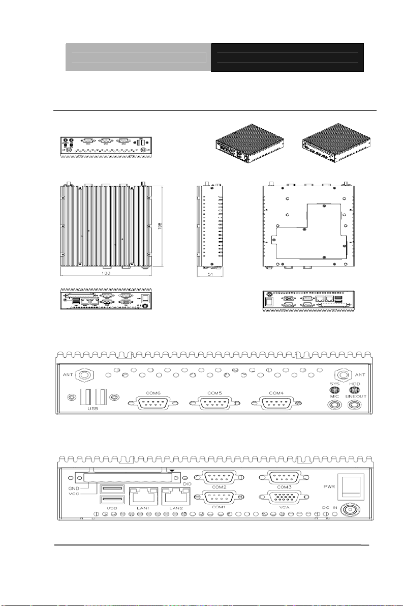
2.1 Dimension and I/O of TKS-G21-CV05
Front side
Back side
Chapter 2 Quick Installation Guide 2 - 2
Page 17
Embedded Box TKS-G21-CV05
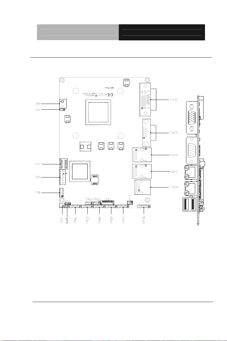
2.2 Location of Connectors and Jumpers of the Main Board
Component Side
Chapter 2 Quick Installation Guide 2 - 3
Page 18
Embedded Box TKS-G21-CV05
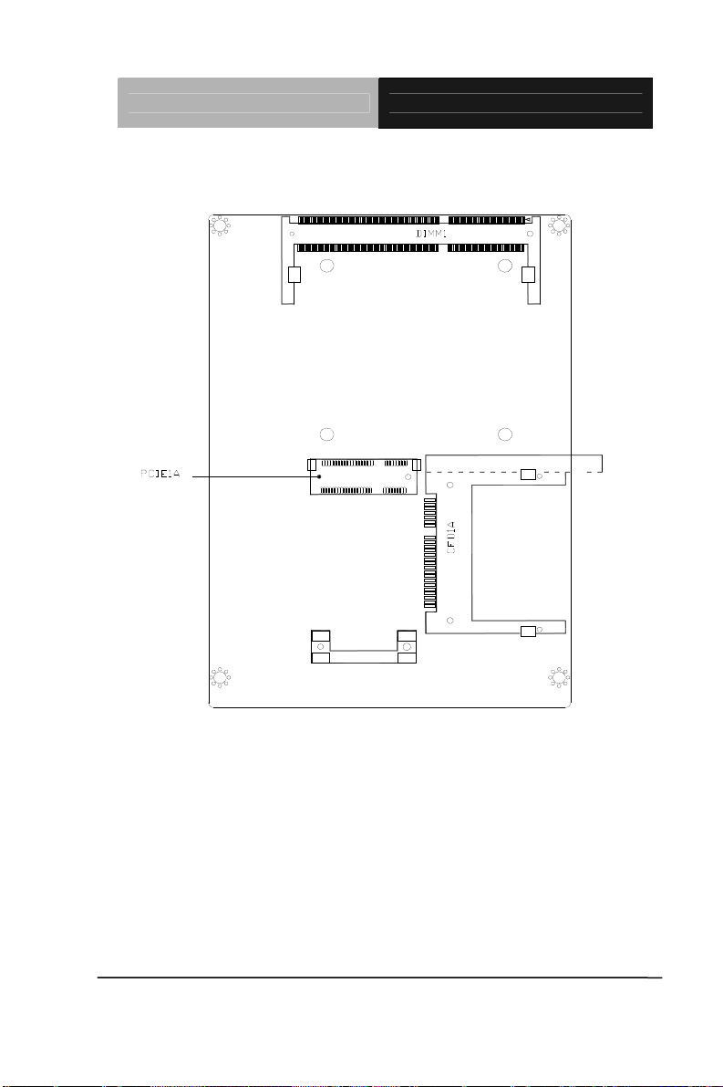
Solder Side
Chapter 2 Quick Installation Guide 2 - 4
Page 19

Embedded Box TKS-G21-CV05
2.3 List of Jumpers
The board has a number of jumpers that allow you to configure your
system to suit your application.
The table below shows the function of each of the board's jumpers:
Label Function
JP1 Auto Power Button Selection
JP2 Clear CMOS
JP3 COM2 RI/+5/+12V Selection
2.4 List of Connectors
The board has a number of connectors that allow you to configure your
system to suit your application.
The table below shows the function of each of the board's connectors:
Label Function CN1 Front Panel
CN5 SATA Port
CN6 External 12V Input
CN7 Digital I/O
CN9 +5V Output for SATA HDD using
CN11 COM Port #6
CN13 COM Port #5
CN16 COM Port #4
CN18 COM Port #3
CN19 COM Port #2
Chapter 2 Quick Installation Guide 2 - 5
Page 20

Embedded Box TKS-G21-CV05
CN28 2
CN29 1st RJ-45 Ethernet
CN30 USB Port #1 and #2
CN31 Audio Line In/Out and MIC
CN32 CRT/DVI (Configured by manufacturing)
CN33 COM Port #1
CFD1 CFAST
PCIE1 Mini Card/mSATA (Configured by Manufacturing)
DIMM1 DDR3 SODIMM Slot
nd
RJ-45 Ethernet
Chapter 2 Quick Installation Guide 2 - 6
Page 21

Embedded Box TKS-G21-CV05
2.5 COM Port #2 RS-232/422/485 Selection (CN19)
COM2 RS-232/422/485 selection for AAEON TKS series is set in BIOS setting
as following:
Entering BIOS Setting Menu: Choose "Integrated Peripherals Super IO
device COM2 select". (Default setting is at "RS-232")
Different devices implement the RS-232/422/485 standard in different ways. If
you have problems with a serial device, check the pin assignments below for
the connector.
RS-232 Mode
Pin Signal Pin Signal
1 DCDB 2 DSRB
3 RXB 4 RTSB
5 TXB 6 CTSB
7 DTRB 8 RIB / +5 Volt. / (+12 Volt.)
9 Ground 10 N/C
RS-422 Mode
Pin Signal Pin Signal
1 TXD- 2 N/C
3 RXD+ 4 N/C
Chapter 2 Quick Installation Guide 2 - 7
Page 22

Embedded Box TKS-G21-CV05
5 TXD+ 6 N/C
7 RXD- 8 N/C / +5 Volt. / (+12 Volt.)
9 Ground 10 N/C
RS-485 Mode
Pin Signal Pin Signal
1 TXD- 2 N/C
3 N/C 4 N/C
5 TXD+ 6 N/C
7 N/C 8 N/C / +5 Volt. / (+12 Volt.)
9 Ground 10 N/C
Note:
Issue: COM port limitation for the speed test during the communication.
Root Cause:
In serial communication, data bits received at the serial port are bundled
into a byte and transmitted into the serial port hardware buffer. From the
buffer, the byte is sent into the CPU. If a new byte arrives before the byte
in the buffer is moved into the CPU, a Hardware Overrun Error occurs.
Solution:
1. Try hardware handshaking.
2. See if the UART is an older un-buffered version or a new buffered
UART (such as a 16550A or 16750). You should use a buf fered UART
for the reasons discussed above.
3. Change the Receive (Rx Trigger) buffer to 8, 4, or 1 (1 is a last resort).
4. For the product, the speed setting of Series Port (COM) is under
9600bps.
Chapter 2 Quick Installation Guide 2 - 8
Page 23

Embedded Box TKS-G21-CV05
2.6 Digital I/O Connector (CN7)
Note: The max. rating of Pin 1 ~ Pin 8 is 3.3V@8mA
The max. rating of Pin 9 is 3.3V@0.5A
This connector offers 4-pair of digital I/O functions.
BIOS using the I2C Bus to read/write internal DIO registers and the Serial Bus
address is 0x6E.
The pin definitions are illustrated below:
Pin Signal Pin Signal
1 Port 1 2 Port 2
3 Port 3 4 Port 4
5 Port 5 6 Port 6
7 Port 7 8 Port 8
9 +3.3V 10 Ground
BIOS Setting
(I2C address)
Connector
Definition
Address(Register)
Output Input
F75111 GPIO Setting
Port 1 @6Eh Pin 1 21h/Bit 0 22h/Bit 0 U44 Pin 6 (GPIO 20)
Port 2 @6Eh Pin 2 21h/Bit 1 22h/Bit 1 U44 Pin 7 (GPIO 21)
Port 3 @6Eh Pin 3 21h/Bit 2 22h/Bit 2 U44 Pin 8 (GPIO 22)
Port 4 @6Eh Pin 4 21h/Bit 3 22h/Bit 3 U44 Pin 24(GPIO 23)
Port 5 @6Eh Pin 5 21h/Bit 4 22h/Bit 4 U44 Pin 23(GPIO 24)
Port 6 @6Eh Pin 6 21h/Bit 5 22h/Bit 5 U44 Pin 22(GPIO 25)
Port 7 @6Eh Pin 7 21h/Bit 6 22h/Bit 6 U44 Pin 21(GPIO 26)
Port 8 @6Eh Pin 8 21h/Bit 7 22h/Bit 7 U44 Pin 20(GPIO 27)
Chapter 2 Quick Installation Guide 2 - 9
Page 24

Embedded Box TKS-G21-CV05
2.7 Hard Disk Installation
Step 1: Unfasten the screws on the top of the heat-sink and you will see the
inside of the system.
Chapter 2 Quick Installation Guide 2 - 10
Page 25

Embedded Box TKS-G21-CV05
Step 2: Fasten the four HDD screws and black damper, and then you can
put the HDD on the opposite side for screwing it up.
Chapter 2 Quick Installation Guide 2 - 11
Page 26

Embedded Box TKS-G21-CV05
Step 3: Putting the HDD with the HDD bracket in by 45 degree height and
make sure the bracket holes are matched with the chassis stand.
Step 4: Screwing the HDD bracket up and connecting the HDD cables with the
MB (GENE-CV05).
Chapter 2 Quick Installation Guide 2 - 12
Page 27

Embedded Box TKS-G21-CV05
Step 5: Putting the chassis heat-sink on the top and fastening the screws up.
Chapter 2 Quick Installation Guide 2 - 13
Page 28

Embedded Box TKS-G21-CV05
2.8 Accessory Installation
Step 1: Unfasten the 5 screws where is on the bottom of the box.
Step 2: You can see the inside placement of RAM, CFast card, PCIe slot for
you installation.
PCIe
RAM
CFast
Card
Chapter 2 Quick Installation Guide 2 - 14
Page 29

Embedded Box TKS-G21-CV05
Step 2-1: Locate the memory module, insert the gold colored contact into the
Socket. Push the module down, until it is firmly seated by locking Two latches
on the sides.
Step 2-2: Locate the mini card module, insert the gold colored contact into the
Socket. Push the module down, until it is firmly seated by locking two latches
on the sides.
Chapter 2 Quick Installation Guide 2 - 15
Page 30

Embedded Box TKS-G21-CV05
Step 2-3: Insert the Compact-Fast card into the socket until t is firmly seated,
and then put the card bracket and screws it up.
Chapter 2 Quick Installation Guide 2 - 16
Page 31

Embedded Box TKS-G21-CV05
2.9 Wallmount Kit Installation
Get the brackets ready and fasten appropriate four screws on each bracket.
After fastening the two brackets on the bottom lid of, the wall mount kits
installation has been finished.
Chapter 2 Quick Installation Guide 2 - 17
Page 32

Embedded Box TKS-G21-CV05
Chapter
3
AMI
BIOS Setup
Chapter 3 AMI BIOS Setup 3-1
Page 33

Embedded Box TKS-G21-CV05
3.1 System Test and Initialization
These routines test and initialize board hardware. If the routines
encounter an error during the tests, you will either hear a few short
beeps or see an error message on the screen. There are two kinds
of errors: fatal and non-fatal. The system can usually continue the
boot up sequence with non-fatal errors.
System configuration verification
These routines check the current system configuration against the
values stored in the CMOS memory. If they do not match, the
program outputs an error message. You will then need to run the
BIOS setup program to set the configuration information in memory.
There are three situations in which you will need to change the
CMOS settings:
1. You are starting your system for the first time
2. You have changed the hardware attached to your system
3. The CMOS memory has lost power and the configuration
information has been erased.
The TKS-G21-CV05 CMOS memory has an integ ral lithium battery
backup for data retention. However, you will need to replace the
complete unit when it runs down.
Chapter 3 AMI BIOS Setup 3-2
Page 34

Embedded Box TKS-G21-CV05
3.2 AMI BIOS Setup
AMI BIOS ROM has a built-in Setup program that allows users to
modify the basic system configuration. This type of information is
stored in battery-backed CMOS RAM so that it retains the Setup
information when the power is turned off.
Entering Setup
Power on the computer and press <Del> or <F2> immediately. This
will allow you to enter Setup.
Main
Set the date, use tab to switch between date elements.
Advanced
Advanced BIOS Features Setup including TPM, ACPI, etc.
Chipset
Host bridge parameters.
Boot
Enables/disable quiet boot option.
Security
Set setup administrator password.
Save&Exit
Exit system setup after saving the changes.
Note:
1. If the "Control LVDS2 (CH7511)" has been set "Disable," and then, the
screen cannot be switched to LVDS2 under the OS.
Chapter 3 AMI BIOS Setup 3-3
Page 35

Embedded Box TKS-G21-CV05
2. If the "Control LVDS2 (CH7511)" has been set "Enable," and then, the
screen can be switched to LVDS2 under the OS.
3. This model does not support LVDS2 output under DOS mode. So if it is a
dual LVDS application, users have to enable “Onboard LVDS 2” on the
LVDS1 panel under BIOS interface, and then, enter to the OS.
4. For LVDS1 + LVDS2 application, this model does not support scaling
after entering the OS, users have to set the fixed resolution on their LCD
Panel under BIOS interface, and then, enter to the OS.
Chapter 3 AMI BIOS Setup 3-4
Page 36

Embedded Box TKS-G21-CV05
Chapter
4
Driver
Inst
allation
Chapter 4 Driver Installation 4 - 1
Page 37

Embedded Box TKS-G21-CV05
The TKS-G21-CV05 comes with a CD-ROM that contains all
drivers and utilities that meet your needs.
Follow the sequence below to install the drivers:
Step 1 – Install Chipset Driver
Step 2 – Install VGA Driver
Step 3 – Install LAN Driver
Step 4 – Install Audio Driver
Step 5 – Install AHCI Driver
Step 6 – Install Wireless LAN Driver (Optional)
Chapter 4 Driver Installation 4 - 2
Page 38

Embedded Box TKS-G21-CV05
4.1 Installation:
Insert the TKS-G21-CV05 CD-ROM into the CD-ROM Drive. And
install the drivers from Step 1 to Step 6 in order.
Step 1 – Install Chipset Driver
1. Click on the STEP1-CHIPSET folder and double click on
the Setup.exe
2. Follow the instructions that the window shows
3. The system will help you install the driver automatically
Step 2 – Install VGA Driver
1. Click on the STEP2-VGA folder and double click on the
Setup.exe
2. Follow the instructions that the window shows
3. The system will help you install the driver automatically
Step 3 – Install LAN Driver
1. Click on the STEP3-LAN folder and double click on the
setup.exe
2. Follow the instructions that the window shows
3. The system will help you install the driver automatically
Step 4 – Install Audio Driver
1. Click on the STEP4-AUDIO folder and double click on the
Setup.exe
2. Follow the instructions that the window shows
3. The system will help you install the driver automatically
Chapter 4 Driver Installation 4 - 3
Page 39

Embedded Box TKS-G21-CV05
Step 5 – Install AHCI Driver
1. Click on the STEP5-AHCI folder and double click on the
setup.exe
2. Follow the instructions that the window shows
3. The system will help you install the driver automatically
Step 6 – Install Wireless LAN Driver (Optional)
1. Click on the STEP6-WIRELESS LAN folder and select
the folder of WLAN or BT_7.4.0.98
2. For WLAN, select the folder of WLAN, and then select the
folder of Install_CD. Double click on the setup.exe file
located in the folder of Install_CD.
For Bluetooth, select the folder of BT_7.4.0.98, and
double click on the Bluetooth_Suite_win7.exe file
3. Follow the instructions that the window shows
4. The system will help you install the driver automatically
Chapter 4 Driver Installation 4 - 4
Page 40

Embedded Box TKS-G21-CV05
A
Appendix
Programming the
atchdog Timer
W
Appendix A Programming the Watchdog Timer A-1
Page 41

Embedded Box TKS-G21-CV05
A.1 Programming
TKS-G21-CV05 utilizes ITE 8783 chipset as its
watchdog timer controller. Below are the procedures to complete
its configuration and the AAEON initial watchdog timer
program is also attached based on which you can
develop customized program to fit your application.
Configuring Sequence Description
After the hardware reset or power-on reset, the ITE 8783 enters the
normal mode with all logical devices disabled except
KBC. The initial state (enable bit ) of this logical device (KBC) is
determined by the state of pin 121 (DTR1#) at the falling edge of
the system reset during power-on reset.
Appendix A Programming the Watchdog Timer A-2
Page 42

Embedded Box TKS-G21-CV05
There are three steps to complete the configuration setup: (1) Enter
the MB PnP Mode; (2) Modify the data of configuration re gisters; (3)
Exit the MB PnP Mode. Undesired result may occur if the MB PnP
Mode is not exited normally.
(1) Enter the MB PnP Mode
To enter the MB PnP Mode, four special I/O write operations are to
be performed during Wait for Key st ate. To ensure the initial state of
the key-check logic, it is necessary to p erform four write opera-tio ns
to the Special Address port (2EH). Two dif f erent enter keys are
provided to select configuration ports (2Eh/2Fh) of the next step.
(2) Modify the Data of the Regist ers
All configuration registers can be accessed after entering the MB
PnP Mode. Before accessing a selected register, the content of
Index 07h must be changed to the LDN to which the register
belongs, except some Global registers.
(3) Exit the MB PnP Mode
Set bit 1 of the configure control register (Index=02h) to 1 to exit the
MB PnP Mode.
Appendix A Programming the Watchdog Timer A-3
Page 43

Embedded Box TKS-G21-CV05
WatchDog Ti mer Configuration Registers
Configure Control (Index=02h)
This register is write only. Its values are not sticky; that is to say, a
hardware reset will automatically clear the bits, and does not
require the software to clear them.
Watch Dog Timer 1, 2, 3 Control Register (Index=71h,81h,91h
Default=00h)
Appendix A Programming the Watchdog Timer A-4
Page 44

Embedded Box TKS-G21-CV05
Watch Dog Timer 1, 2, 3 Configuration Register (Index=72h,
82h, 92h Default=001s0000b)
Watch Dog Timer 1,2,3 Time-Out Value (LSB) Register
(Index=73h,83h,93h, Default=38h)
Watch Dog Timer 1,2,3 Time-Out Value (MSB) Register
(Index=74h,84h,94h Default=00h)
Appendix A Programming the Watchdog Timer A-5
Page 45

Embedded Box TKS-G21-CV05
A.2 ITE8783 Watchdog Timer Initial Program
.MODEL SMALL
.CODE
Main:
CALL Enter_Configuration_mode
CALL Check_Chip
mov cl, 7
call Set_Logic_Device
;time setting
mov cl, 10 ; 10 Sec
dec al
Watch_Dog_Setting:
;Timer setting
mov al, cl
mov cl, 73h
call Superio_Set_Reg
;Clear by keyboard or mouse interrupt
mov al, 0f0h
mov cl, 71h
call Superio_Set_Reg
;unit is second.
mov al, 0C0H
mov cl, 72h
Appendix A Programming the Watchdog Timer A-6
Page 46

Embedded Box TKS-G21-CV05
call Superio_Set_Reg
; game port enable
mov cl, 9
call Set_Logic_Device
Initial_OK:
CALL Exit_Configuration_mode
MOV AH,4Ch
INT 21h
Enter_Configuration_Mode PROC NEAR
MOV SI,WORD PTR CS:[Offset Cfg_Port]
MOV DX,02Eh
MOV CX,04h
Init_1:
MOV AL,BYTE PTR CS:[SI]
OUT DX,AL
INC SI
LOOP Init_1
RET
Enter_Configuration_Mode ENDP
Exit_Configuration_Mode PROC NEAR
MOV AX,0202h
Appendix A Programming the Watchdog Timer A-7
Page 47

Embedded Box TKS-G21-CV05
CALL Write_Configuratio n_Data
RET
Exit_Configuration_Mode ENDP
Check_Chip PROC NEAR
MOV AL,20h
CALL Read_Configuration_Data
CMP AL,87h
JNE Not_Initial
MOV AL,21h
CALL Read_Configuration_Data
CMP AL,81h
JNE Not_Initial
Need_Initial:
STC
RET
Not_Initial:
CLC
RET
Check_Chip ENDP
Read_Configuration_Data PROC NEAR
MOV DX,WORD PTR CS:[Cfg_Port+04h]
Appendix A Programming the Watchdog Timer A-8
Page 48

Embedded Box TKS-G21-CV05
OUT DX,AL
MOV DX,WORD PTR CS:[Cfg_Port+06h]
IN AL,DX
RET
Read_Configuration_Data ENDP
Write_Configuration_Data PROC NEAR
MOV DX,WORD PTR CS:[Cfg_Port+04h]
OUT DX,AL
XCHG AL,AH
MOV DX,WORD PTR CS:[Cfg_Port+06h]
OUT DX,AL
RET
Write_Configuration_Data ENDP
Superio_Set_Reg proc near
push ax
MOV DX,WORD PTR CS:[Cfg_Port+04h]
mov al,cl
out dx,al
pop ax
inc dx
out dx,al
ret
Superio_Set_Reg endp.Set_Logic_Device proc near
Appendix A Programming the Watchdog Timer A-9
Page 49

Embedded Box TKS-G21-CV05
Set_Logic_Device proc near
push ax
push cx
xchg al,cl
mov cl,07h
call Superio_Set_Reg
pop cx
pop ax
ret
Set_Logic_Device endp
;Select 02Eh->Index Port, 02Fh->Data Port
Cfg_Port DB 087h,001h,055h,055h
DW 02Eh,02Fh
END Main
Note: Interrupt level mapping
0Fh-Dh: not valid
0Ch: IRQ12
.
.
03h: IRQ3
02h: not valid
01h: IRQ1
00h: no interrupt selected
Appendix A Programming the Watchdog Timer A-10
Page 50

Embedded Box TKS-G21-CV05
Appendix
B
I/O Information
Appendix B I/O Information B - 1
Page 51

Embedded Box TKS-G21-CV05
B.1 I/O Address Map
Appendix B I/O Information B - 2
Page 52

Embedded Box TKS-G21-CV05
Appendix B I/O Information B - 3
Page 53

Embedded Box TKS-G21-CV05
B.2 1st MB Memory Address Map
Appendix B I/O Information B - 4
Page 54

Embedded Box TKS-G21-CV05
B.3 IRQ Mapping Chart
Appendix B I/O Information B - 5
Page 55

Embedded Box TKS-G21-CV05
B.4 DMA Channel Assignments
Appendix B I/O Information B - 6
Page 56

Embedded Box TKS-G21-CV05
A ppendix
C
Digital I/O
Appendix C Digital I/O C-1
Page 57

Embedded Box TKS-G21-CV05
C.1 Digital I/O
The F75111 provides one serial access i nterface, I2C Bus, to read/write
internal registers. The address of Serial Bus is 0x6E (0110_1110)
The related register for configuring DIO is list as follows:
Configuration and Control Register-Index 01h
Power-on default [7:0]=0000_1000b
Bit Name R/W PWR Description
Software reset for all registers
7
6
5
4
INIT
Reserved
EN_WDT10
Reserved
R/W VSB3V
R/W VSB3V
R/W VSB3V
R/W VSB3V
including Test Mode re gisters.
Users use only.
Enable Reset Out. If set to 1,
enable WDTOUT10# output.
Default is disable.
Reserved
3
Reserved
2
SMART_P
1
OWR_MAG
EMENT
SOFT_PO
0
WR_DOWN R/W VSB3V
Appendix C Digital I/O C-2
R/W VSB3V
R/W VSB3V
R/W VSB3V
Set this bit to 1 will enable auto
power down mode, when all
function are idle then 20ms the
chip will auto power down, it will
wakeup when GPIO state change
or read write register
Set this bit to 1 will power down all
of the analog block and stop
internal clock, write 0 to clear this
bit or when GPIO state change will
auto clear this bit to 0.
Page 58

Embedded Box TKS-G21-CV05
GPIO2x Output Control Register-Index 20h
Power-on default [7:0]=0000_0000b
Bit Name R/W PWR Description
GPIO 27 output control. Set to 1
for output function. Set to 0 for
input function (default).
GPIO 26 output control. Set to 1
for output function. Set to 0 for
input function (default).
GPIO 25 output control. Set to 1
for output function. Set to 0 for
input function (default).
GPIO 24 output control. Set to 1
for output function. Set to 0 for
input function (default).
GPIO 23 output control. Set to 1
for output function. Set to 0 for
input function (default).
GPIO 22 output control. Set to 1
for output function. Set to 0 for
input function (default).
GPIO 21 output control. Set to 1
for output function. Set to 0 for
input function (default).
GPIO 20 output control. Set to 1
for output function. Set to 0 for
input function (default).
7
6
5
4
3
2
1
0
GP27_OCT
RL
GP26_OCT
RL
GP25_OCT
RL
GP24_OCT
RL
GP23_OCT
RL
GP22_OCT
RL
GP21_OCT
RL
GP20_OCT
RL
R/W VSB3V
R/W VSB3V
R/W VSB3V
R/W VSB3V
R/W VSB3V
R/W VSB3V
R/W VSB3V
R/W VSB3V
GPIO2x Output Data Register-Index 21h
Power-on default [7:0]=0000_0000b
Bit Name R/W PWR Description
7
6
5
GP27_ODA
TA
GP26_ODA
TA
GP25_ODA
TA
R/W VSB3V
R/W VSB3V
R/W VSB3V
GPIO 27 output data.
GPIO 26 output data.
GPIO 25 output data.
Appendix C Digital I/O C-3
Page 59

Embedded Box TKS-G21-CV05
GP24_ODA
4
TA
GP23_ODA
3
TA
GP22_ODA
2
TA
GP21_ODA
1
TA
GP20_ODA
0
TA
GPIO2x Input Status Register-Index 22h
Power-on default [7:0]=xxxx_xxxxb
Bit Name R/W PWR Description
GP27_PST
7
S
GP26_PST
6
S
GP25_PST
5
S
GP24_PST
4
S
GP23_PST
3
S
GP22_PST
2
S
GP21_PST
1
S
GP20_PST
0
S
R/W VSB3V
R/W VSB3V
R/W VSB3V
R/W VSB3V
R/W VSB3V
RO VSB3V
RO VSB3V
RO VSB3V
RO VSB3V
RO VSB3V
RO VSB3V
RO VSB3V
RO VSB3V
GPIO 24 output data.
GPIO 23 output data.
GPIO 22 output data.
GPIO 21 output data.
GPIO 20 output data.
Read the GPIO27 data on the pin.
Read the GPIO26 data on the pin.
Read the GPIO25 data on the pin.
Read the GPIO24 data on the pin.
Read the GPIO23 data on the pin.
Read the GPIO22 data on the pin.
Read the GPIO21 data on the pin.
Read the GPIO20 data on the pin.
The following is a sample code for 8 input
.MODEL SMALL
.CODE
Appendix C Digital I/O C-4
Page 60

Embedded Box TKS-G21-CV05
begin:
mov cl,01h
mov al,80h
call CT_I2CWriteByte
call Delay5ms
mov al,00h
mov cl,20h
call CT_I2CWriteByte
mov cl,22h
call CT_I2CReadByte
;Input : CL - register index
; CH - devic e ID
;Output : AL - Value read
Ct_I2CReadByte Proc Near
mov ch,06eh
mov dx, 0f000h + 00h ; Host Control Register
mov al, 0ffh ; Clear previous
commands
out dx, al
Appendix C Digital I/O C-5
Page 61

Embedded Box TKS-G21-CV05
call Delay5ms
mov dx, 0f000h + 04h ; Transmit Slave Address
Register
inc ch ; Set the slave address and
mov al, ch ; prepare for a READ command
out dx, al
mov dx, 0f000h + 03h ; Host Command Register
mov al, cl ; offset to read
out dx, al
mov dx, 0f000h + 05h
xor al, al ; Clear old data
out dx, al
mov dx, 0f000h + 02h ; Host Control Reegister
mov al, 48h ; Start a byte access
out dx, al
call CT_Chk_SMBus_Ready
mov dx, 0f000h + 05h
in al, dx
ret
Appendix C Digital I/O C-6
Page 62

Embedded Box TKS-G21-CV05
Ct_I2CReadByte Endp
;Input : CL - register index
; CH - device ID
; AL - Value to write
;Output: none
Ct_I2CWriteByte Proc Near
mov ch,06eh
xchg ah, al
mov dx, 0f000h + 00h ; Host Control Register
mov al, 0ffh ; Clear previous
commands
out dx, al
call Delay5ms
mov dx, 0f000h + 04h ; Transmit Slave Address
Register
mov al, ch ; Set the slave address and
out dx, al ; prepare for a WRITE
command
mov dx, 0f000h + 03h ; Host Command Register
mov al, cl ; offset to write
Appendix C Digital I/O C-7
Page 63

Embedded Box TKS-G21-CV05
out dx, al
mov dx, 0f000h + 05h
mov al, ah
out dx, al
mov dx, 0f000h + 00h ; Host Control Register
mov al, 48h ; Start a byte access
out dx, al
call CT_Chk_SMBus_Ready
ret
Ct_I2CWriteByte Endp
; Wait until the busy bit clears, indicating that the SMBUS
; activity has concluded.
CT_Chk_SMBus_Ready Proc Near
mov dx,0f000h+ 0;status port
clc
mov cx,0800h
Chk_I2c_OK:
in al,dx ;get status
call Delay5ms
Appendix C Digital I/O C-8
Page 64

Embedded Box TKS-G21-CV05
out dx,al ;clear status
call Delay5ms
test al, 02H ;termination of command ?
jnz short Clear_final
and al, NOT 40H ;mask INUSE bit
or al,al ;status OK ?
jz short Clear_final
test al,04h ;device error
jnz short SMBus_Err
loop short Chk_I2c_OK
;SMbus error due to timeout
SMBus_Err:
stc
ret
Clear_final:
clc
ret
CT_Chk_SMBus_Ready Endp
END begin
Appendix C Digital I/O C-9
 Loading...