

Page 1

SBC-556
Half-size CPU Card with
LCD, Ethernet, & SSD
Page 2

FCC STATEMENT
THIS DEVICE COMPLIES WITH P ART 15 FCC RULES. OPERATION IS SUBJECT TO THE FOLLOWING TWO CONDITIONS:
(1) THIS DEVICE MA Y NOT CAUSE HARMFUL INTERFERENCE. (2) THIS DEVICE MUST ACCEPT ANY INTERFERENCE
RECEIVED, INCLUDING INTERFERENCE THA T MA Y CAUSE
UNDESIRED OPERA TION.
THIS EQUIPMENT HAS BEEN TESTED AND FOUND TO
COMPL Y WITH THE LIMITS FOR A CLASS "A" DIGIT AL
DEVICE, PURSUANT TO P AR T 15 OF THE FCC RULES.
THESE LIMITS ARE DESIGNED TO PROVIDE REASONABLE PROTECTION AGAINST HARMFUL INTERFERENCE
WHEN THE EQUIPMENT IS OPERA TED IN A COMMERCIAL ENVIRONMENT . THIS EQUIPMENT GENERA TES,
USES, AND CAN RADIA TE RADIO FREQUENCY ENERGY
AND , IF NOT INST ALLED AND USED IN ACCORDANCE
WITH THE INSTRUCTION MANUAL, MA Y CAUSE
HARMFUL INTERFERENCE TO RADIO COMMUNICATIONS. OPERA TION OF THIS EQUIPMENT IN A RESIDENTIAL AREA IS LIKEL Y TO CAUSE HARMFUL INTERFERENCE IN WHICH CASE THE USER WILL BE REQUIRED
TO CORRECT THE INTERFERENCE A T HIS OWN EXPENSE.
Page 3

Copyright Notice
This document is copyrighted, 1999, by AAEON Technology Inc.
All rights are reserved. AAEON T echnology Inc. reserves the right
to make improvements to the products described in this manual at
any time without notice.
No part of this manual may be reproduced, copied, translated or
transmitted in any form or by any means without the prior written
permission of AAEON Technology Inc. Information provided in
this manual is intended to be accurate and reliable. However,
AAEON Technology Inc. assumes no responsibility for its use, nor
for any infringements upon the rights of third parties which may
result from its use.
Acknowledgements
ALI is a trademark of Acer Laboratories, Inc.
AMD is a trademark of Advanced Micro Devices, Inc.
A ward BIOS is a trademark of A ward Software International, Inc.
AutoCAD and AutoShade are trademarks of Autodesk, Inc.
CHIPS Logotype is a registered trademark; Chips 69000 is a
trademark of Chips and T echnologies, Inc.
Cyrix is a trademark of Cyrix Corporation.
IBM, PC/A T , PS/2 and VGA are trademarks of International
Business Machines Corporation.
Intel and Pentium are trademarks of Intel Corporation.
Lotus, 1-2-3 and Symphony are trademarks of Lotus Development
Corp.
Microsoft Windows®, MS-DOS, Corporation Windows and
Microsoft are registered trademarks of Microsoft Corp.
SiS is a trademark of Silicon Integrated System Corp.
SMC is a trademark of Standard Microsystems Corporation.
TurboDLD Classic is a trademark of Panacea Inc.
UMC is a trademark of United Microelectronics Corporation.
W ordPerfect is a trademark of W ordPerfect Corporation.
VESA® is a registered trademark of Video Electronics Standards
Association.
All other product names or trademarks are properties of their
respective owners.
Part No. 2047556002 SBC-556 A1.0 3rd Edition
Printed in T aiwan March 1999
Page 4

Packing list
Before you begin installing your card, please make sure that the
following materials have been shipped:
• 1 SBC-556 CPU card
•1
• 1 6-pin mini-DIN dual outlet adapter for keyboard and PS/2
mouse
• 1 Hard disk drive (IDE) interface cable (40-pin)
• 1 Floppy disk drive interface cable (34-pin)
• 1 Parallel port adapter (26-pin) and dual outlet adapter . (one for
Rs-232, another one for RS-422/485)
• 1 CD-ROM Utilities
• 4 Utility disks with CHIPS 69000 utility programs and drivers
If any of these items are missing or damaged, contact your distributor or sales representative immediately.
Page 5

Notice
Dear Customer,
Thank you for purchasing the SBC-556 board. The user
manual is designed to help you to get the most out of the SBC556, please read it thoroughly before you install and use the
board. The product that you have purchased comes with a one-year
warranty, but AAEON cannot be responsible for misuse of the
product. Therefore, we strongly urge that the first read the
manual before using the product.
To receive the lastest version of the user manual, please visit our
Web site at:
Taiwan: www.aaeon.com.tw
U.S.A : www.aaeon.com
Page 6

Contents
Chapter 1: General Information ....................... 1
Introduction ........................................................................... 2
Features.................................................................................. 3
Specifications ......................................................................... 4
Board layout........................................................................... 6
Card dimensions .................................................................... 7
Chapter 2: Installation ....................................... 9
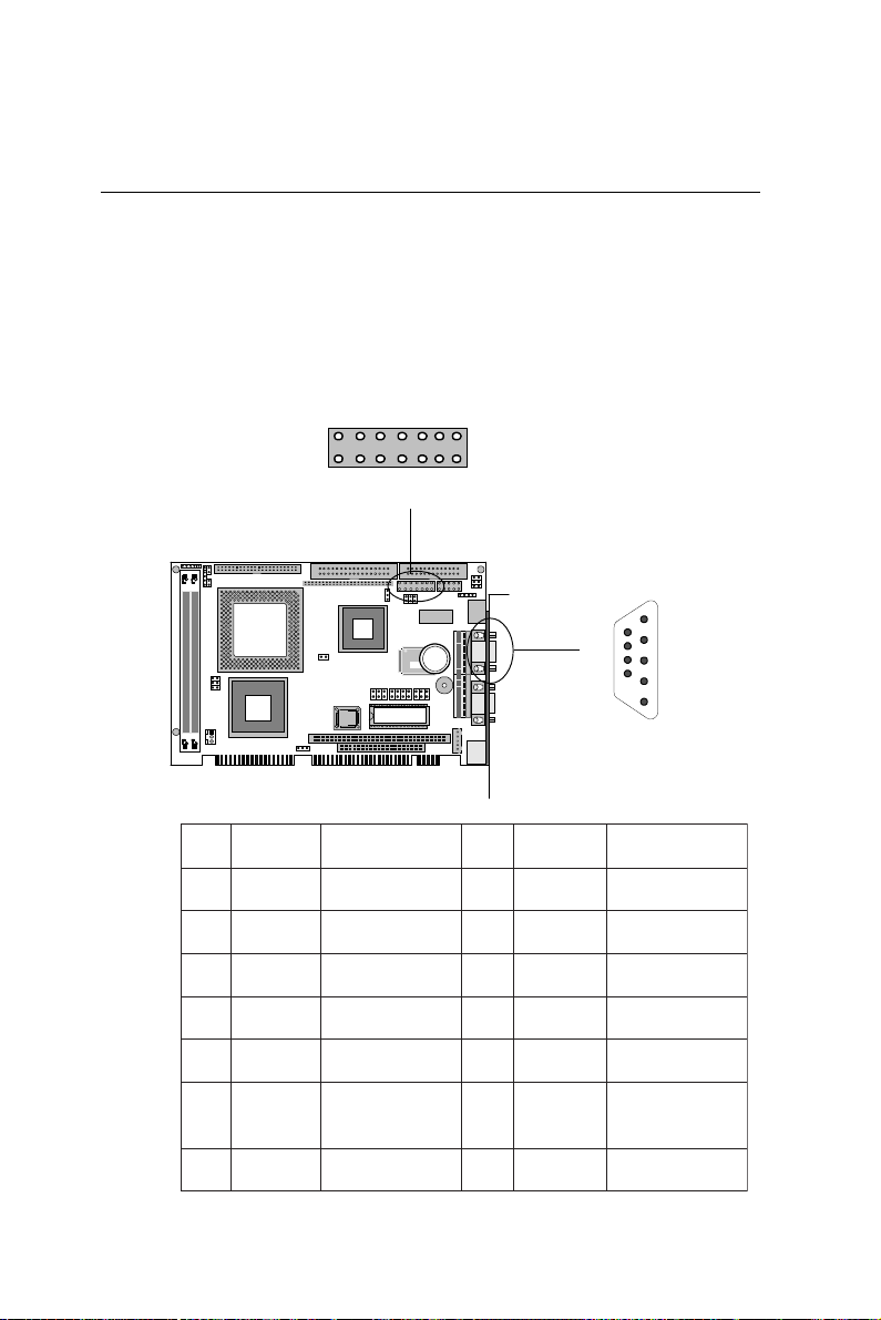
Jumpers and connectors .................................................... 1 0
Locating jumpers and connectors .................................... 1 2
Setting jumpers ................................................................... 1 3
Safety precautions ............................................................... 1 4
Installing the CPU ............................................................... 1 4
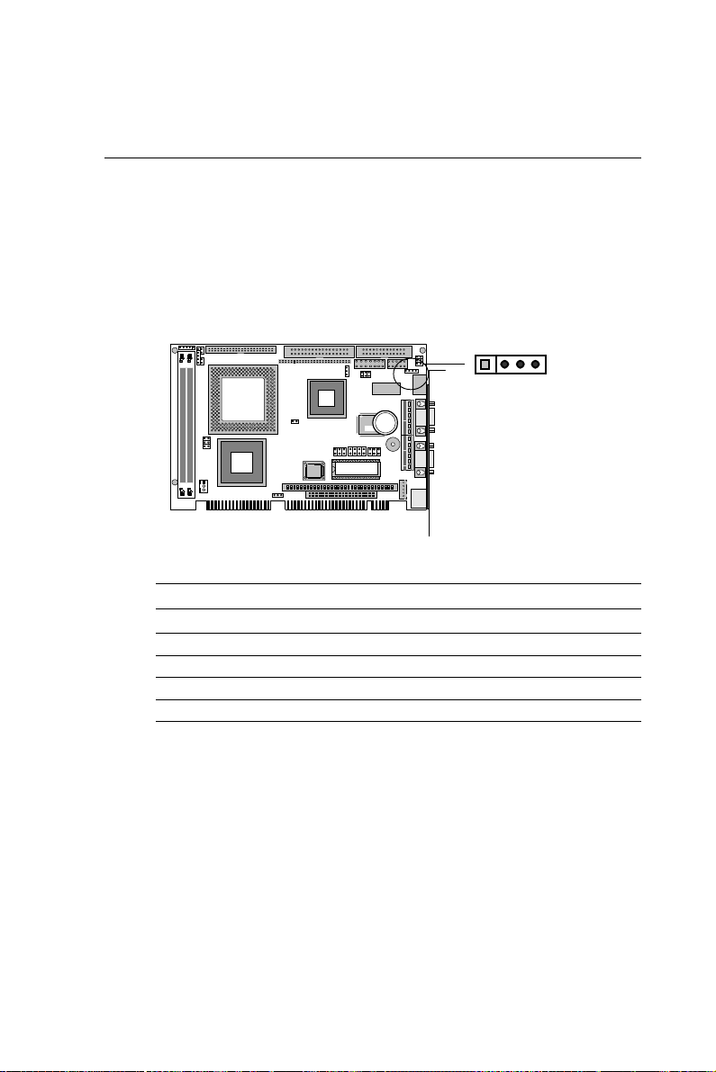
CPU clock ratio (JP1) .........................................................1 6
DRAM voltage setting (JP2) ........................................... 1 7
RS-232/422/485 select (COM2)(JP3).............................. 1 8
CPU VIO voltage setting (JP4) ........................................ 1 9
IR connector (Reserved)(JP5) ......................................... 2 0
CPU external clock select (JP6) ...................................... 21
CPU Vcore voltage select (JP7) ....................................... 23
DOC address select (JP8) ................................................. 25
Ethernet active/link signal LED (JP9)(JP10)(JP11) ..... 2 6
Clear CMOS data (JP12) ................................................... 2 7
LCD inverter connector (CN1) ........................................ 2 8
Power LED and keylock connector (CN2) ..................... 2 9
IDE LED connector (CN3) ................................................ 30
Hardware reset connector (CN4) ..................................... 3 1
IDE hard drive connector (CN5) ...................................... 3 2
Fan power connector (CN6) .............................................. 3 4
Floppy drive connector (CN7) .......................................... 3 5
Parallel (Printer) port connector (CN8) ........................... 3 7
Page 7

Display connectors (CN9, CN15) ..................................... 3 8
Serial ports connectors (CN10, CN14) ............................ 4 1
USB connectors (dual-port) (CN11) ................................. 4 2
Ethernet connector (CN12) ............................................... 4 3
Power connectors (P8 & P9)(CN13) ................................ 44
KB & PS/2 Mouse connector (CN17) ............................. 4 5
DiskOnChip socket ............................................................ 4 7
Chapter 3: Award BIOS Setup .......................... 49
System test and initialization ............................................. 5 0
System configuration verification ............................................50
AWARD BIOS setup ........................................................... 5 1
Entering setup..........................................................................51
Standard CMOS setup ....................................................... 5 2
BIOS festures setup ........................................................... 5 3
Virus Warning..........................................................................54
Chipset features setup ....................................................... 5 6
Power management setup .................................................. 5 8
PM timers................................................................................60
PM Events ............................................................................... 61
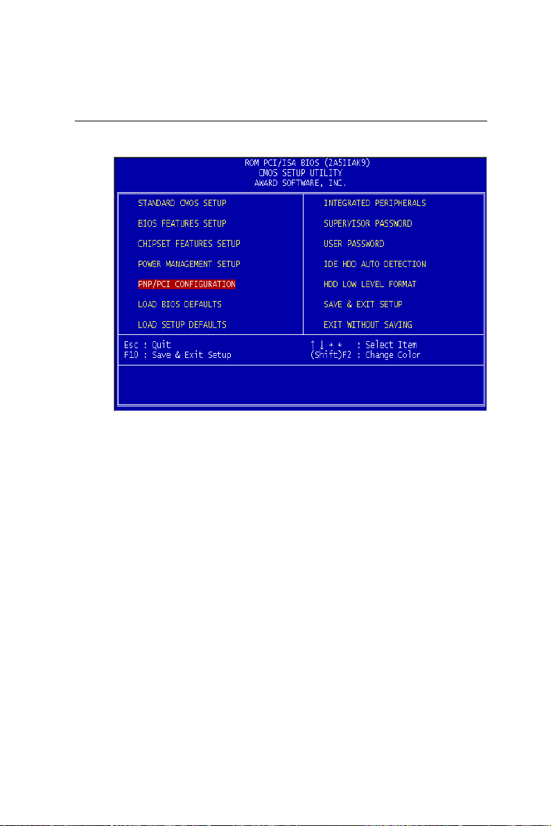
PnP/PCI Configuration setup ............................................ 6 2
Load BIOS DEFAULT / LOAD SETUP DEFAULTS ... 65
Integrated Peripherals ....................................................... 6 6
Supervisor/User Password setting ................................... 7 0
Auto detect hard disk ......................................................... 7 2
HDD low level format......................................................... 73
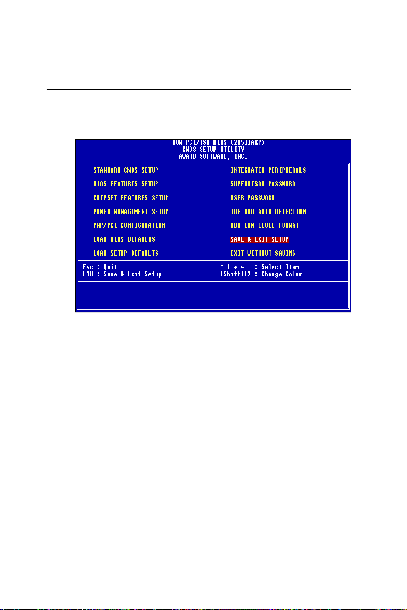
Save & exit setup ................................................................ 7 4
Page 8

Exit without saving ............................................................. 7 5
Chpater 4: Flat Panel/CRT Controller Display
Drivers and Utilities ......................77
Software drivers .................................................................. 7 8
Hardware configuration ..........................................................7 8
Necessary prerequisites .......................................................... 79
Before you begin .....................................................................79
Ò
9595
. .. . .. ... .. . .. ... .. . .. ... .. . .. ... .. . .. ... .. . .. ... .. . .. ... .. . .. ... .. . .. .. .. . .. ... .. . .. ... .. . .. ... .. . .. ... .. . .. ... .. . .. ... .. . .. ... .. . .. ... .. . .. .
95
Windows
Windows
. .. . .. ... .. . .. ... .. . .. ... .. . .. ... .. . .. ... .. . .. ... .. . .. ... .. . .. ... .. . .. . 80
9595
. .. . .. ... .. . .. ... .. . .. ... .. . .. ... .. . .. ... .. . .. ... .. . .. ... .. . .. ... .. . .. .. .. . .. ... .. . .. ... .. . .. ... .. . .. ... .. . .. ... .. . .. ... .. . .. ... .. . .. ... .. . .. .
Ò
3 . 13 . 1
.. ...................................................................... ....................................................................
3 . 1
.. .................................................................... 88
3 . 13 . 1
.... .................................................................... ....................................................................
OS/2....................................................................................... 89
Windows
NT3.51NT3.51
NT3.51
NT3.51NT3.51
............................................................................................................................
.............................................................. 91
............................................................................................................................
Ò
WindowsÒ NT4.0.................................................................. 92
Chapter 5: Ethernet Software Configuration ...
......................................................... 93
Ethernet software configuration ....................................... 9 4
Appendix A: Programming the Watchdog
Timer .............................................. 95
Programming the watchdog timer .................................... 9 6
How to program the WATCHDOG TIMER...........................96
Demo program ........................................................................97
Appendix B: Installing PC/104 Modules .......... 99
Installing PC/104 modules ............................................... 1 00
Page 9

CHAPTER
General
Information
This chapter provides background
information for the SBC-556.
Sections include:
• Card specifications
• Board layout
1
Chapter 1 General Information 1
Page 10

Introduction
The SBC-556 is an all-in-one single board Pentium computer card.
With an onboard flat panel/CR T SVGA controller , the SBC-556 packs
all the functions of an industrial computer and its display capabilities
onto a single, half-size card. This means the SBC-556 is your absolute
best solution for embedded applications.
The onboard PCI-bus, flat panel/CRT SVGA controller uses the CHIPS
69000 chipset with 2 MB of SDRAM built in chip. This chipset, used
with local PCI-bus, is a 64-bit graphics engine. Excellent for displayintensive applications, this card supports various LCD types, including TFT , DSTN, MONO, and EL.
Another feature of the SBC-556 is the inclusion of a high speed, local
bus IDE controller. This controller supports (through ATA PIO) mode
3 and mode 4 hard disks, and Ultra DMA/33, enabling data transfer
rates up to 33 MB/second. Up to two IDE devices can be connected,
including large hard disks, CD-ROM drives, tape backup drives, or
other IDE devices.
Onboard features include two high-speed RS-232 serial ports with
16C550 UART s, one bidirectional SPP/EPP/ECP parallel port, and one
floppy drive controller. In addition, the SBC-556 includes an extra 512
KB of second level on-board cache memory.
If program execution is halted by a program bug or EMI, the board's
watchdog timer can automatically reset the CPU or generate an
interrupt. This ensures reliability in unmanned or stand alone systems.
The SBC-556 supports 5V EDO DRAM. It also provides two 72-pin
SIMM (Single In-line Memory Module) sockets for its onboard
system DRAM. These sockets give you the flexibility to configure
your system from 8 MB to 128 MB of DRAM using the most
economical combination of SIMMs.
2 SBC-556 User Manual
Page 11

Features
• DiskOnChip (SSD) up to 144MB
• C&T 69000 LCD controller supports 36-bit TFT panels.
• 100Base-T Fast Ethernet
• PC/104 expansion connector
• Optional function to support L VDS (Low Voltage Differential Signaling) for
high-speed and low-power data transfer.
Chapter 1 General Information 3
Page 12

Specifications
CPU: Intel Pentium 75~200 MHz, P55C(MMX) 166~233 MHz, Cyrix / IBM /
SGS 6X86 PR100+~166+, AMD K5 PR75~166, K6 PR2 166~300
Bus interface: ISA
CPU Socket: Intel Socket 7
BIOS: 256KB FLASH BIOS
Chipset: SiS5582
Super I/O Chipset: Winbond W83877 with Fully 16-bit I/O decoded
Level 2 Cache: Onboard 512 KB pipeline burst 2nd level cache
System memory: 8 MB to 128 MB. T wo 72-pin SIMM socket onboard
Enhanced IDE hard disk drive interface: Supports up to two hard disk drives.
Supports PIO mode 4 and Bus Master. Also supports Multi-word DMA and
Ultra DMA/33
Floppy disk drive interface: supports up to two floppy disk drives, 5.25"(360
KB and 1.2 MB) and/or 3.5" (720 KB, 1.44 MB and 2.88 MB)
Multi-mode parallel port: Configured to LPT1, LPT2, LPT3 or disabled.
Supports SPP , ECP, and EPP.
Serial ports: One RS-232 and one RS-232/422/485 serial port. Ports can be
configured as COM1, COM2, COM3, COM4 or disabled individually. T w o
16C550 serial UARTs. IR connector reserved for future use.
Keyboard/mouse connector: 6-pin mini DIN connector supports PC/A T
standard keyboard and PS/2 mouse.
USB connectors: Dual USB connectors onboard
Battery: Lithium battery for data retention of up to 10 years
Watchdog T imer: Can generate a system reset, IRQ15 or NMI. Supports
Win95, W in3.1. Software selectable timeout interval (1 sec. ~ 255 sec.,
1sec./step).
DMA channels: 7
Interrupt levels: 15
4 SBC-556 User Manual
Page 13

Power management: I/O peripheral devices support power saving and doze/
standby/suspend modes. APM 1.2 compliant.
PC/104 connector: 104-pin connector for a 16-bit bus
Ethernet interface
Chipset: Realtek RTL8139A 100/10 Base-Tx Fast Ethernet controller.
Ethernet interface: Onboard 100/10 Base-T RJ-45 connector.
Flat panel VGA interface
Chipset: C&T 69000
Display memory: 2 MB SDRAM built in Chip
Display type: Supports CRT and flat panel (TFT , DSTN, MONO and EL)
display. Can display both CRT and flat panel simultaneously .
Resolution: Supports up to 1024x768 @ 64K colors.
SSD interface
One 32-pin DIP socket supports M-System DiskOnChip 2000 series, memory
capacity from 2 MB to 144 MB
Chapter 1 General Information 5
Page 14

Mechanical and environmental
Power supply voltage: +5V (4.75V to 5.25V)
+12V (11.4V to 12.6V)
Power Requirement:
Bare Bone power consumption: +5V @ 1.5A
Power Requirement (with Pentium MMX): +5V @ 6A
Power Requirement (with K6-233): +5V @ 10A
Operating temperature: 32 to 140OF ( 0 to 60OC )
Board size: 7.3" (L) x 4.8" (W) (185 mm x 122 mm)
Board weight: 1.32 lb. (0.6 Kg)
6 SBC-556 User Manual
Page 15
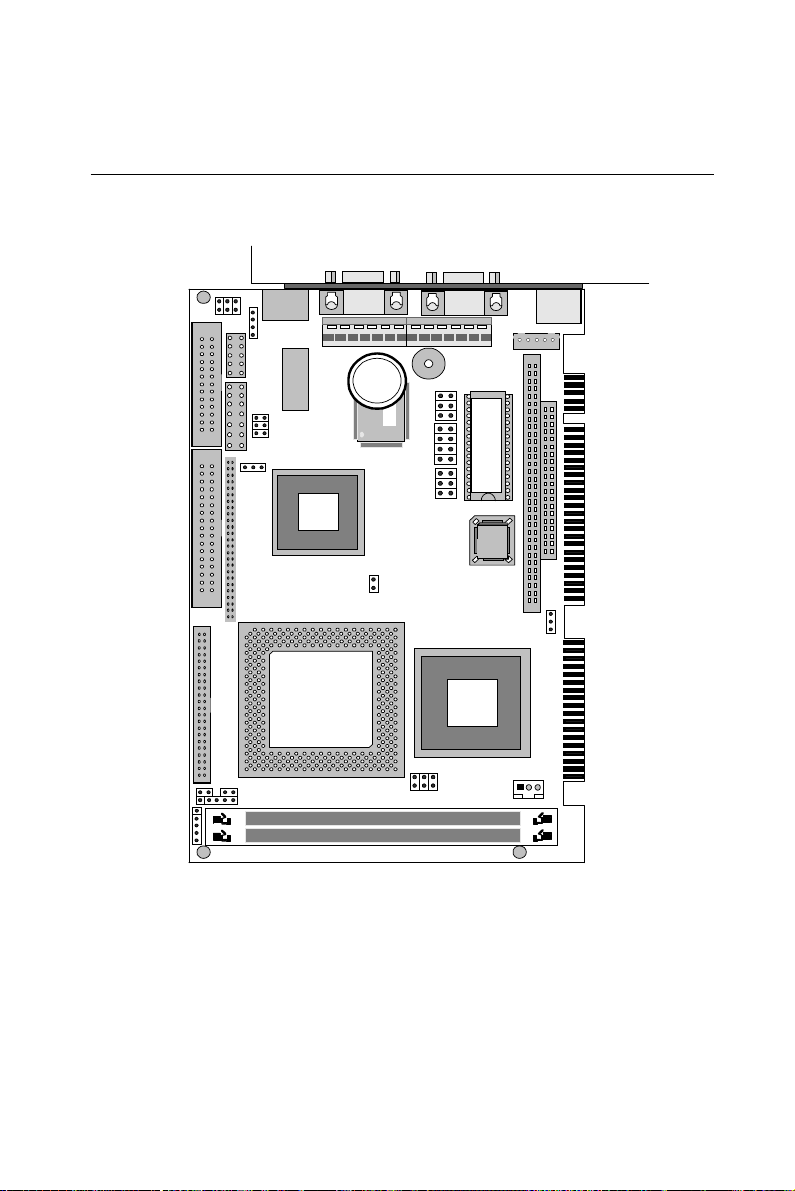
Board layout
B69000
CHIPS
Winbond
BAT
DiskOnChip
5582
SIS
Chapter 1 General Information 7
Page 16
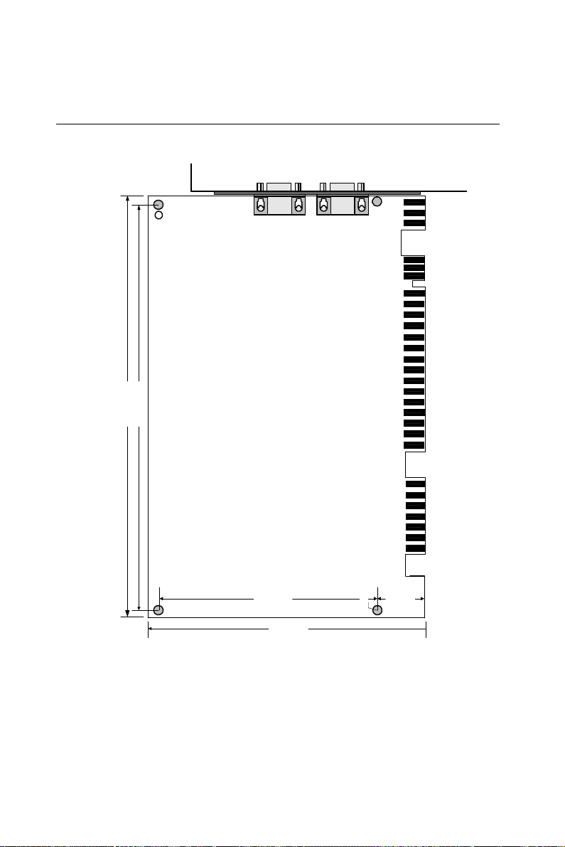
Card dimensions
185.00
178.00
8 SBC-556 User Manual
98.50 19.50
D4x4
122.00
Page 17

2
CHAPTER
Installation
This chapter explains set-up procedures
for the SBC-556 hardware, including
instructions on setting jumpers and
connecting peripherals, switches, and
indicators. Be sure to read all safety
precautions before you begin the installation procedure.
Chapter 2 Installation 9
Page 18

Jumpers and connectors
Connectors on the board link it to external devices such as hard
disk drives, keyboard, or floppy drives. In addition, the board has a
number of jumpers that allow you to configure your system to suit
your applications.
The table below lists the function of each of the jumpers and
connectors:
Jumpers
Label Function
JP1 CPU clock ratio
JP2 LCD driving voltage select
JP3 RS-232/422/485 select (COM2)
JP4 CPU VIO voltage setting
JP5 IR connector (Reserved)
JP6 CPU external clock select
JP7 CPU Vcore voltage select
JP8 DOC address select
JP9 Ethernet RX signal LED connector
JP10 Ethernet Linkage signal LED connector
JP11 Externet TX signal LED connector
JP12 Clear CMOS data
10 SBC-556 User Manual
Page 19

connector
Label Function
CN 1 LCD inverter power connector
CN 2 Powe LED & keylock connector
CN 3 IDE LED connector
CN 4 Hardware reset connector
CN 5 IDE hard drive connector
CN 6 Fan power connector
CN 7 Floppy drive connector
CN 8 Parallel (Printer) port connector
CN 9 LCD panel connector
CN10 RS-232/422/485 connector (COM2)
CN11 USB connectors (dual-port)
CN12 Ethernet connector
CN13 Power connectors (P8 & P9)
CN14 COM1 connector
CN15 VGA connector
CN16 External Keyboard connector
CN17 KB & PS/2 mouse connector
Chapter 2 Installation 11
Page 20
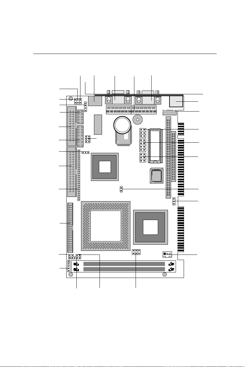
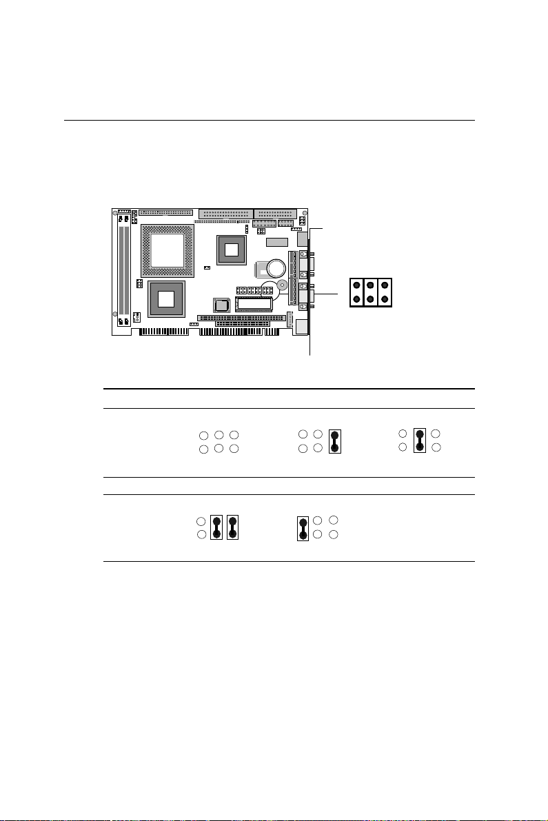
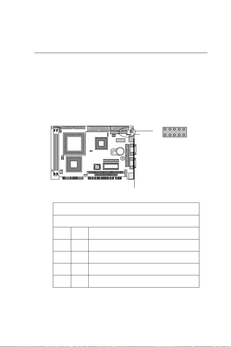
Locating jumpers and connectors
JP10
JP9
JP5
CN11
CN8
CN10
JP2
CN7
CN9
CN5
JP11
CN12
JP3
CN14
B69000
CHIPS
CN13
Winbond
BAT
CN15
DiskOnChip
5582
SIS
CN17
CN16
JP8
JP7
JP6
JP4
JP12
CN3
CN1
CN2
CN4
12 SBC-556 User Manual
CN6
JP1
Page 21
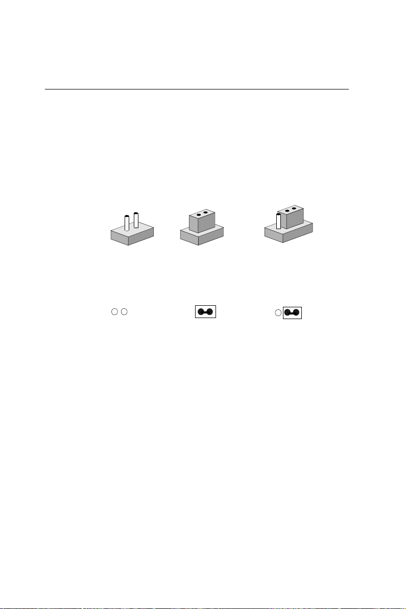
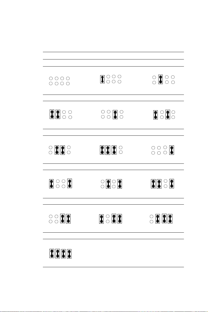
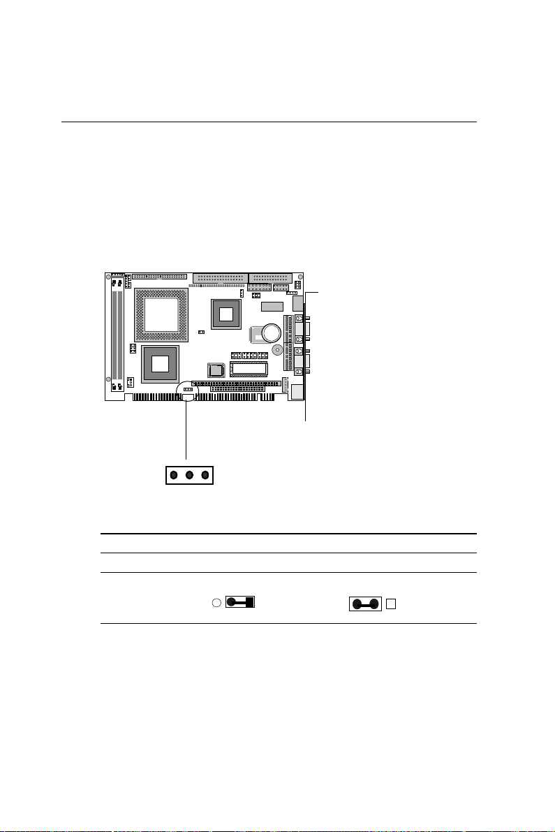
Setting jumpers
You configure your card to match the needs of your application by
setting jumpers. A jumper is the simplest kind of electric switch. It
consists of two metal pins and a small metal clip (often protected
by a plastic cover) that slides over the pins to connect them. To
close a jumper you connect the pins with the clip. To "open" a
jumper you remove the clip. Sometimes a jumper will have three
pins, labeled 1, 2, and 3. In this case, you would connect either pins
1 and 2 or 2 and 3.
1
Open Closed Closed 2-3
The jumper settings are schematically depicted in this manual as
follows:
1 2 3
Open Closed Closed 2-3
A pair of needle-nose pliers may be helpful when working with
jumpers.
3
2
If you have any doubt about the best hardware configuration for
your applications, contact your local distributor or sales representative before you make any change.
Generally, you simply need a standard cable to make most connections.
Chapter 2 Installation 13
Page 22

Safety precautions
Warning! Always completely disconnect the power cord from
your chassis whenever you are working on it. Do
not make connections while the power is on
because sensitive electronic components can be
damaged by the sudden rush of power. Only
experienced electronics personnel should open
the PC chassis.
Caution! Always ground yourself to remove any static
charge before touching the CPU card. Modern
electronic devices are very sensitive to static
electric charges. Use a grounding wrist strap at all
times. Place all electronic components on a
static-dissipative surface or in a static-shielded
bag when they are not in the chassis.
Installing the CPU
The SBC-556 CPU card supports most Pentiums and their compatible CPUs. The system's performance depends on the CPU you
choose. You can install or upgrade the CPU in the board's PGA
socket by following the procedures outlined below. If your system
has an existing CPU, you need to remove it before installing the
new CPU.
Removing a CPU
1. Disconnect power from the chassis, and unplug all connections
to the CPU card. Then, remove the CPU card from the chassis
by following the instructions in the user's manual for your
chassis.
2 . Lift the CPU out of the PGA socket. The old chip may be
difficult to remove. Y ou may find spray chip lubricant, designed
for pin-grid-array (PGA) devices, and a chip puller helpful.
These are available at electronics hobbyists' supply stores.
14 SBC-556 User Manual
Page 23

Installing a CPU
T o install the CPU, follow the instructions that came with it. If no
documentation was provided, the general procedures for installing
a CPU are outlined below:
1 . Lubricate the pins on the CPU with lubricant for PGA devices.
This makes the CPU slide in much easier and greatly reduces
the chance of damaging the pins and other components.
2 . Carefully align the CPU so that it is parallel to the socket. Make
sure that the notch on the corner of the CPU matches the notch
on the inside of the socket.
3 . Gently push the CPU into the socket. There will probably be a
small gap between the CPU and the socket even when it is fully
seated. DO NOT USE EXCESSIVE FORCE!
When you install a new CPU, you may have to adjust other
settings on the board, such as CPU type, CPU clock, and PCI
speed, to accommodate it. Make sure that the settings are correct
for your CPU. Improper settings may damage the CPU.
Chapter 2 Installation 15
Page 24
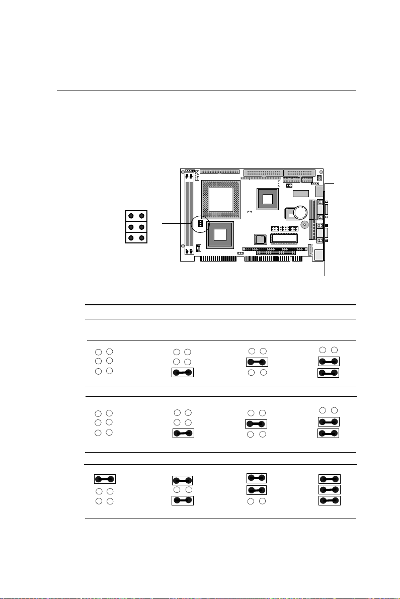
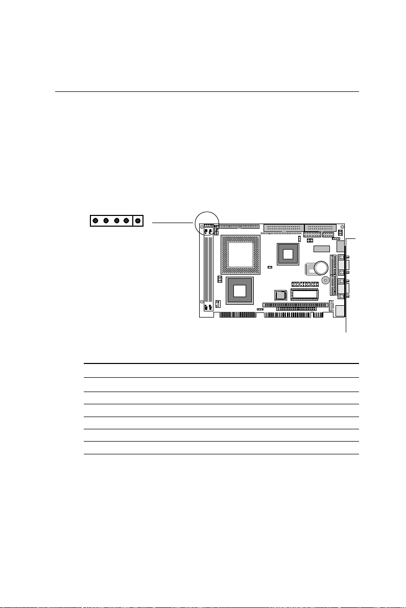
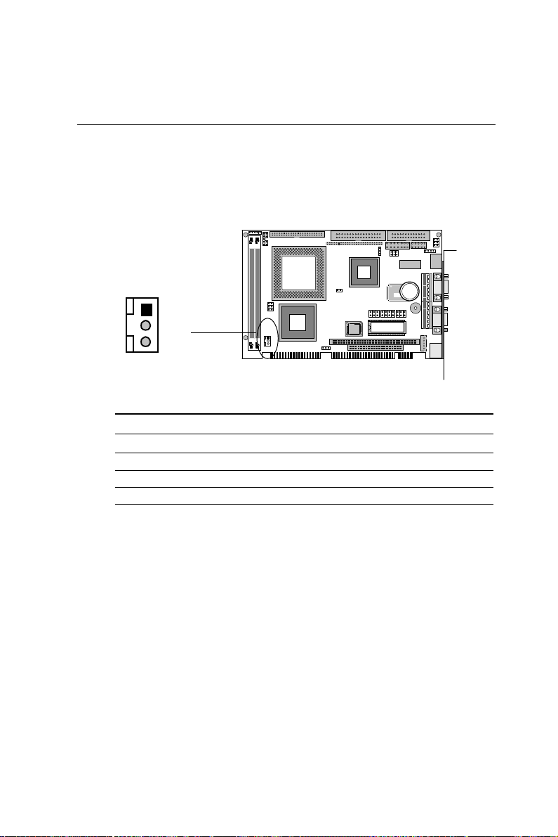
CPU clock ratio (JP1)
JP1 must be set to match the CPU clock ratio. The chart below
shows the proper jumper settings for P54C, P55C, and AMD-K6,
and their respective clock ratio.
CHIPS
B69000
1
3
5
CPU Clock Ratio (JP1)
P54C x1.5 P54C x2.0 P54C x3.0 P54C x2.5
P55C x3.5 P55C x2.0 P55C x3.0 P55C x2.5
2
1
4
3
5
6
2
4
6
1
3
5
5582
SIS
2
4
6
1
3
5
DiskOnChip
2
4
6
*
BAT
Winbond
2
1
4
3
5
6
AMD-K6 x3.5 AMD-K6 x2.0 AMD-K6 x3.0 AMD-K6 x2.5
2
1
4
3
5
6
1
3
5
2
4
6
2
1
4
3
5
6
AMD-K6 x5.5 AMD-K6 x4.0 AMD-K6 x5.0 AMD-K6 x4.5
2
1
3
5
2
4
6
2
1
4
3
5
6
1
4
3
6
5
*default
16 SBC-556 User Manual
2
1
4
3
5
6
1
3
5
2
4
6
Page 25
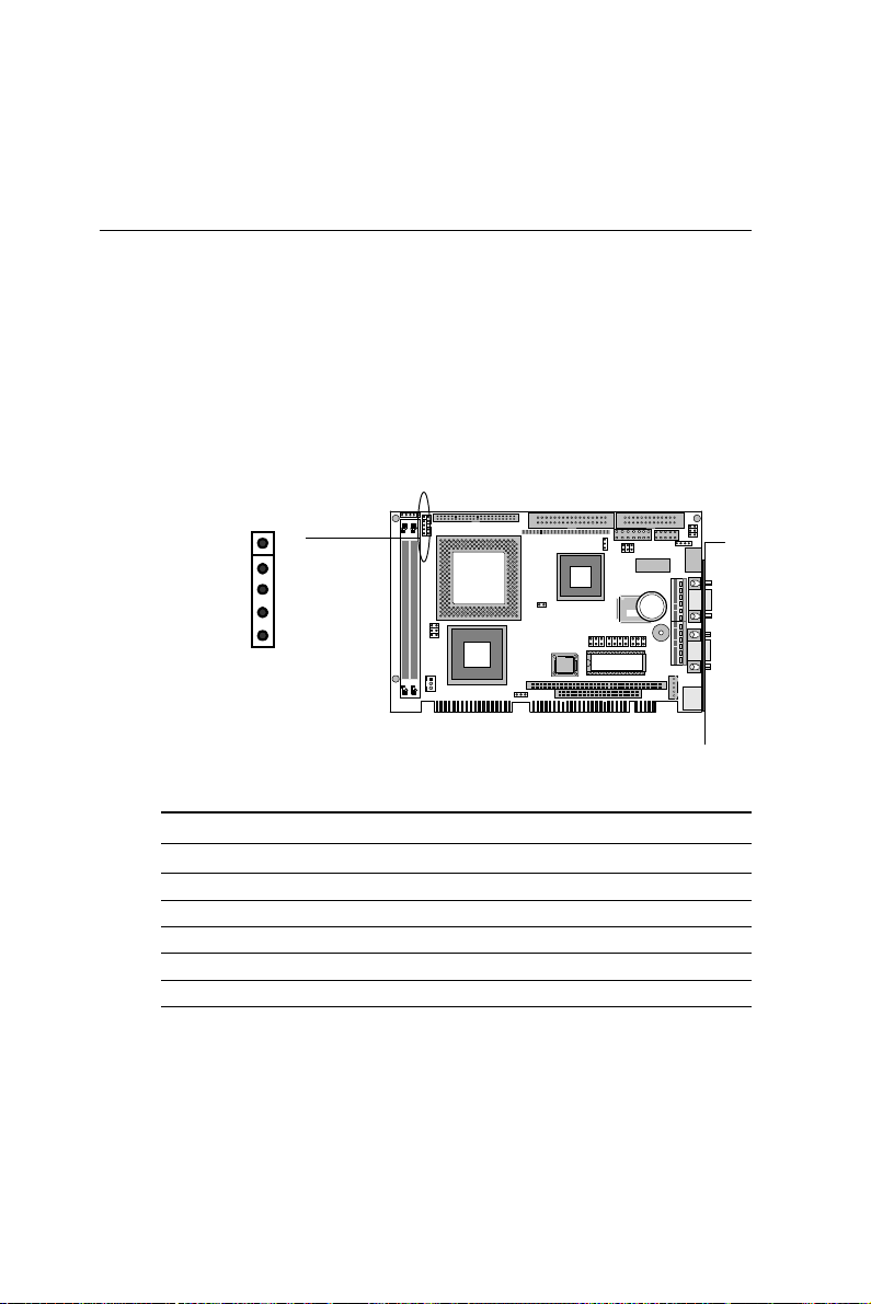
LCD driving voltage setting (JP2)
JP2 allows users to select the LCD driving voltage.
The configurations as belows:
1
CHIPS
B69000
BAT
Winbond
5582
SIS
DiskOnChip
LCD driving voltage setting (JP2)
5 V * 3.3V
1
2
3
*default
2
3
1
2
3
Chapter 2 Installation 17
Page 26
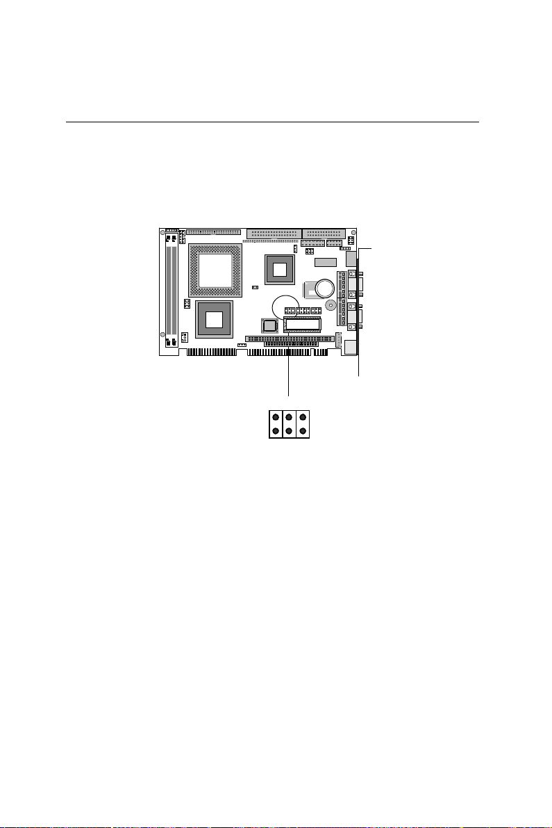
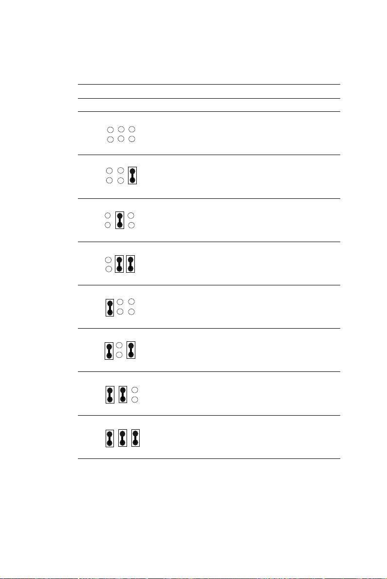
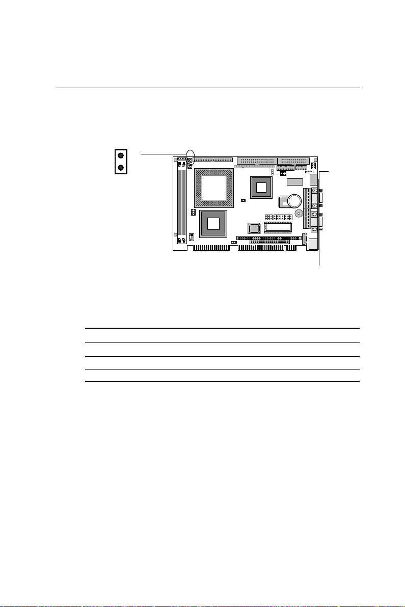
RS-232/422/485 select (COM2)(JP3)
The COM2 can be configured to operate in RS-232, RS-422, or RS485 mode. The operation mode can be set via JP3.
2 4 6
CHIPS
B69000
BAT
Winbond
5582
SIS
DiskOnChip
RS-232* RS-422 RS-485
2 4 6
2 4 6
1 3 5
2 4 6
1 3 5
*default
18 SBC-556 User Manual
1 3 5
1 3 5
Page 27
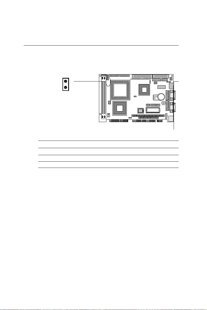
CPU VIO voltage setting (JP4)
JP4 must be set to match the CPU type. The chart below shows the
proper jumper settings for their respective CPU I/O voltage:
CHIPS
B69000
5582
SIS
CPU VIO voltage setting (JP4)
3.5 V 3.3 V*
*default
DiskOnChip
BAT
Winbond
Chapter 2 Installation 19
Page 28
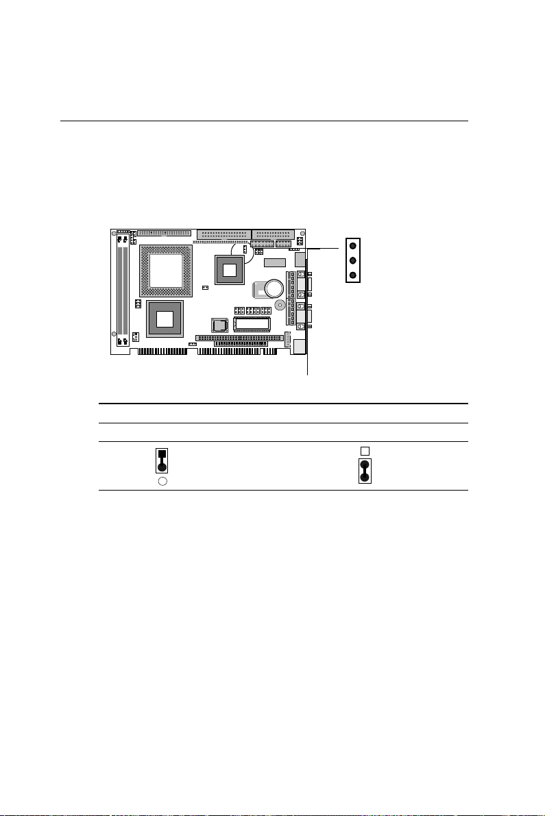
IR connector (Reserved)(JP5)
The onboard IR connector supports an Infra-Red port module that
enables wireless communication between the computer and other
computers and devices with infrared capability. The port module is
an optional component. If it is installed, you must set the IR
Transfer Mode in the Peripheral section of the CMOS setup utility.
CHIPS
B69000
BAT
Winbond
5582
SIS
DiskOnChip
IR connector (JP5)
Pin Function
1RX
2 GND
3TX
45V
1 2 3 4
20 SBC-556 User Manual
Page 29
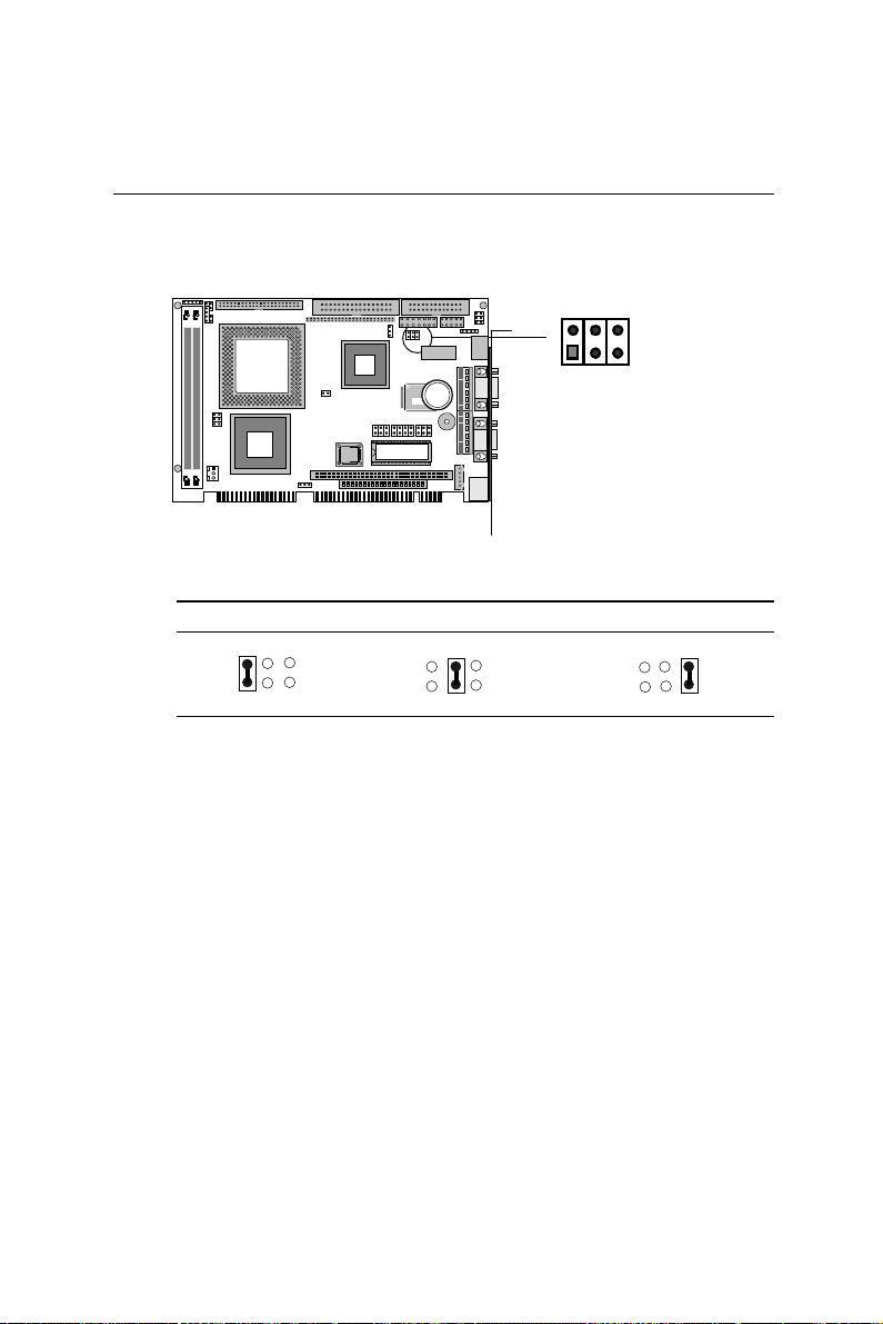
CPU external clock select (JP6)
The JP6 is used to sychronize the system clock with the CPU type.
You may need to adjust the CPU clock according the base CPU
speed.
CHIPS
B69000
BAT
Winbond
5582
SIS
DiskOnChip
2 4 6
1 3 5
Chapter 2 Installation 21
Page 30
CPU External clock select (JP6)
JP6 CPU PCI BUS
2 4 6
*
66.8M 33.4M
1 3 5
2 4 6
60M 30M
1 3 5
2 4 6
75M 37.5M
1 3 5
2 4 6
83.8M 33.3M
1 3 5
2 4 6
68.5M 34.5M
1 3 5
2 4 6
83.8M 41.65M
1 3 5
2 4 6
75M 32M
1 3 5
2 4 6
1 3 5
*default
22 SBC-556 User Manual
50M 25M
Page 31
CPU Vcore voltage select (JP7)
The JP7 must be set to match the CPU type.
The chart below shows the proper jumper settings for their
respective Vcc.
CHIPS
B69000
BAT
Winbond
5582
SIS
DiskOnChip
2 4 6 8
1 3 5 7
Chapter 2 Installation 23
Page 32
CPU Vcore Voltage settings (JP7)
2.0 V 2.1 V 2.2 V
2 4 6 8
1 3 5 7
2 4 6 8
1 3 5 7
2 4 6 8
1 3 5 7
2.3 V 2.4V 2.5V
2 4 6 8
1 3 5 7
2 4 6 8
1 3 5 7
2 4 6 8
1 3 5 7
2.6 V 2.7 V 2.8 V
2 4 6 8
1 3 5 7
2 4 6 8
1 3 5 7
2 4 6 8
1 3 5 7
2.9 V 3.0V 3.1 V
2 4 6 8
1 3 5 7
2 4 6 8
1 3 5 7
2 4 6 8
1 3 5 7
3.2 V 3.3V 3.4 V
2 4 6 8
2 4 6 8
2 4 6 8
*
1 3 5 7
3.5 V
2 4 6 8
1 3 5 7
*default
24 SBC-556 User Manual
1 3 5 7
1 3 5 7
Page 33
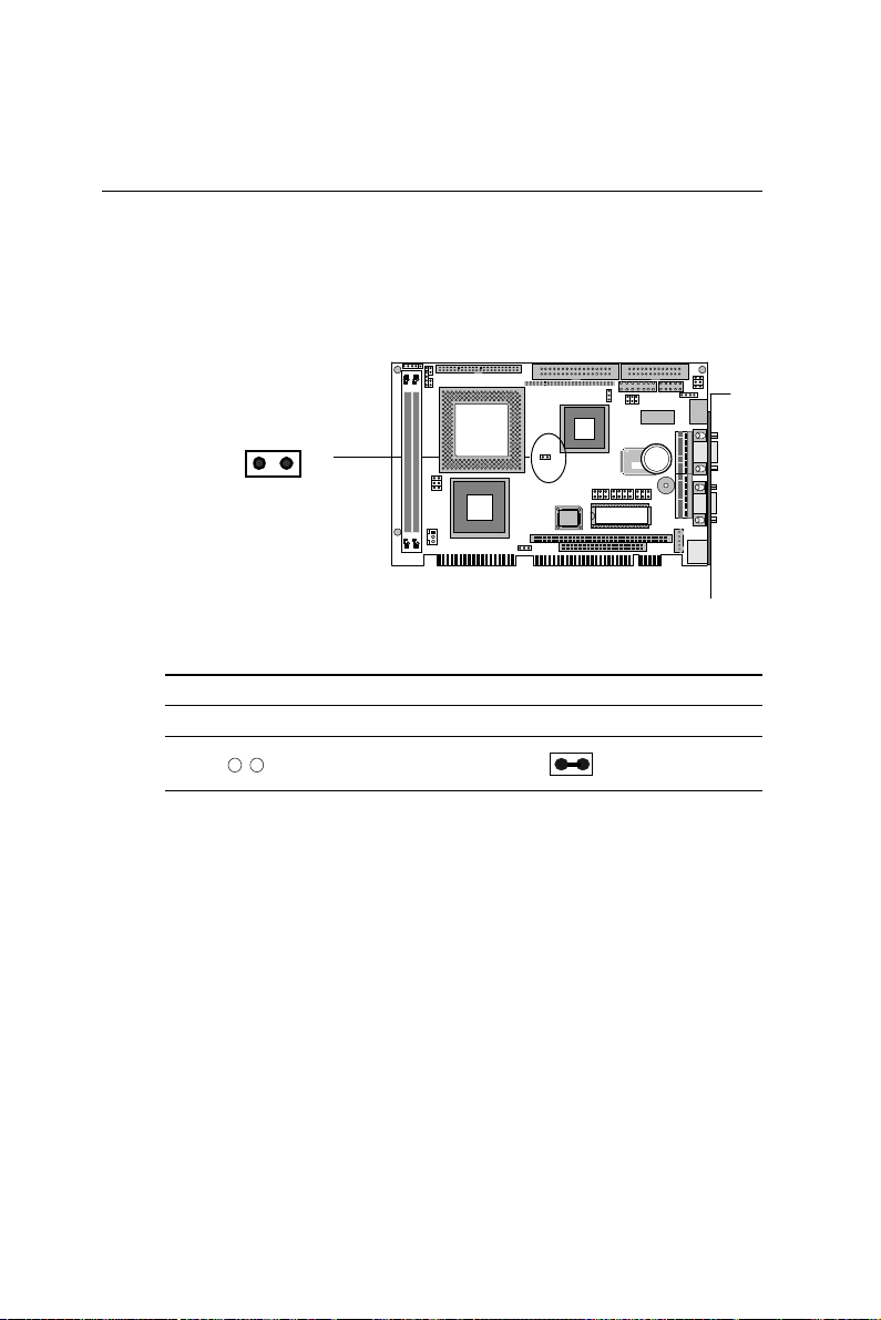
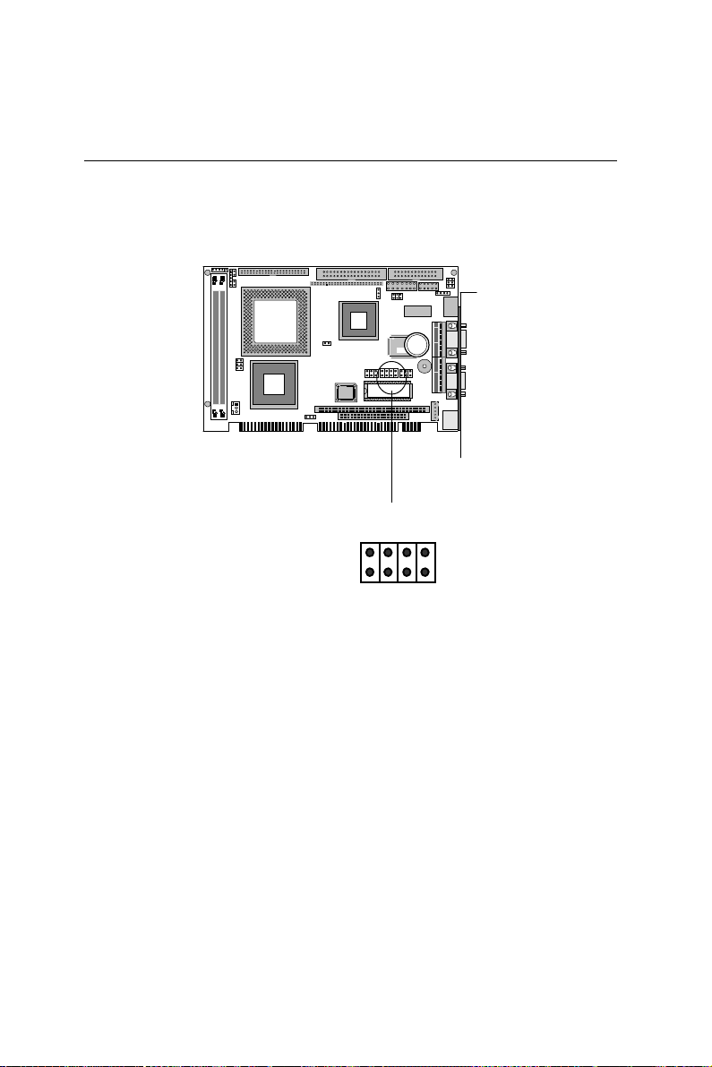
DOC address select (JP8)
The DiskOnChip 2000 occupies an 8 K byte window in the upper
memory address range of CC00 to DC00. Y ou should ensure this
does not conflict with any other device's memory address.
CHIPS
B69000
BAT
Winbond
5582
SIS
DiskOnChip
Address CC00 D000 D400
2 4 6
2 4 6
2 4 6
1 3 5
2 4 6
1 3 5
1 3 5
1 3 5
Address D800* DC00
2 4 6
1 3 5
2 4 6
1 3 5
*default
These addresses might conflict with the ROM BIOS on some of the
other peripheral boards. Please select appropriate memory address
to avoid memory conflict.
Chapter 2 Installation 25
Page 34
Ethernet active/link signal LED
(JP9)(JP10)(JP11)
The mainboard can connect three LED indicators to show the
status of the communication link and traffic. The functions are
showed as follows:
Ethernet active signal LED (JP9)(JP11)
A flashing LCD indicates that the SBC-556 is transmitting (JP11) or
receiving (JP9) data.
Ethernet link signal LED (JP10)
A continuously lit LED indicates good linkage between the SBC556 and its supporting hub.
CHIPS
B69000
BAT
Winbond
5582
SIS
DiskOnChip
JP9
JP10
JP11
26 SBC-556 User Manual
Page 35
Clear CMOS data (JP12)
Y ou can connect an external jumper cap or switch to clear CMOS.
Clear CMOS procedure:
1. Disconnect all power source.
2. Move JP12 from 1-2 to 2-3 for few seconds.
3. Move JP12 back to 1-2.
CHIPS
B69000
BAT
Winbond
5582
SIS
3 2 1
DiskOnChip
Clear CMOS data (JP12)
Project * Clear CMOS data
J12
3 2 1
*default
3 2 1
Chapter 2 Installation 27
Page 36
LCD inverter power connector (CN1)
The CN1 is a 5-pin invertor connector which could provide the
power for LCD invertor. The following table shows the pin assignments of CN1. The pin-5 “BKL_ON” is normally active “high”.
Please refer to “Power Management Setup” in the BIOS SETUP
Menu and select “LCD off Option” to enable power management.
CN1 offers LCD backlight control signals for your applications.
The pin assignments are as follows:
5 4 3 2 1
CHIPS
B69000
BAT
Winbond
5582
SIS
LCD inverter power connector (CN1)
Pin Function
1 +12V
2 GND
3 GND
4NC
5 +5V
DiskOnChip
28 SBC-556 User Manual
Page 37
Power LED and keylock connector
(CN2)
Y ou can connect an LED to indicate when the CPU card is on. Pin 1
of CN2 supplies power to the LED; Pin 3 is the ground.
You can use a switch (or a lock) to disable the keyboard. In this
state, the PC will not respond to any input. This is useful if you do
not want anyone to change or stop a running program. Simply
connect the switch between Pins 4 and 5. The pin assignments
appear in the following table:
1
2
3
4
5
5582
SIS
CHIPS
B69000
DiskOnChip
BAT
Winbond
Power LED and keylock connector (CN2)
Pin Function
1 LED Power (+5 V)
2 No Connector
3 Ground
4 Keyboard lock
5 Ground
Chapter 2 Installation 29
Page 38
IDE LED connector (CN3)
Y ou can connect an LED to indicate that an IDE device is in
use.The pin assignments for this connector are as follows:
1
2
CHIPS
5582
SIS
IDE LED connector (CN3)
Pin Function
1 -R/W IDE
2 Pull high (Vcc)
B69000
DiskOnChip
BAT
Winbond
30 SBC-556 User Manual
Page 39
Hardware reset connector (CN4)
You can connect an LED to indicate that an IDE device is in use.
The pin assignments for this connector are as follows:
1
2
Hardware reset connector (CN4)
Pin Function
1 Reset
2 Ground
SIS
5582
CHIPS
B69000
DiskOnChip
BAT
Winbond
Chapter 2 Installation 31
Page 40

IDE hard drive connector (CN5)
You can attach one or two Enhanced Integrated Device Electron-ics
hard disk drives to the SBC-556’s internal controller . The SBC-556’ s
IDE controller uses a PCI local-bus interface and supports faster
data transfer.
Connecting the hard drive
Connecting drives is done in a daisy-chain fashion and requires
one of two cables, depending on the drive size. 1.8" and 2.5" drives
need a 1 x 44-pin to 2 x 44-pin flat-cable connector. 3.5" drives use a
1 x 44-pin to 2 x 40-pin connector.
Wire number 1 on the cable is red or blue, and the other wires are
gray .
1. Connect one end of the cable to CN5. Make sure that the red (or
blue) wire corresponds to pin 1 on the connector, which is
labeled on the board (on the right side).
2. Plug the other end of the cable to the Enhanced IDE hard drive,
with pin 1 on the cable corresponding to pin 1 on the hard drive.
(See your hard drive’s documentation for the location of the
connector.)
Connect a second drive as described above.
Unlike floppy drives, IDE hard drives can connect to either end of
the cable. If you install two drives, you will need to set one as the
master and one as the slave by using jumpers on the drives. If you
install just one drive, set it as the master.
32 SBC-556 User Manual
Page 41

Pin assignments
The following table lists the pin numbers and their respective
signals:
IDE Connector (CN5)
Pin Signal Pin Signal
1 Reset 2 GND
3D7 4D8
5D6 6D9
7 D5 8 D10
9D4 10D11
11 D3 12 D12
13 D2 14 D13
15 D1 16 D14
17 D0 18 D15
19 GND 20 N.C.
21 N.C. 22 GND
23 IOW 24 GND
25 IOR 26 GND
27 IORDY 28 BALE
29 N.C. 30 GND
31 IRQ 14 32 -I/O CS16
33 A1 34 N.C.
35 A0 36 A2
37 CS0 38 CS1
39 -ACT 40 GND
Chapter 2 Installation 33
Page 42
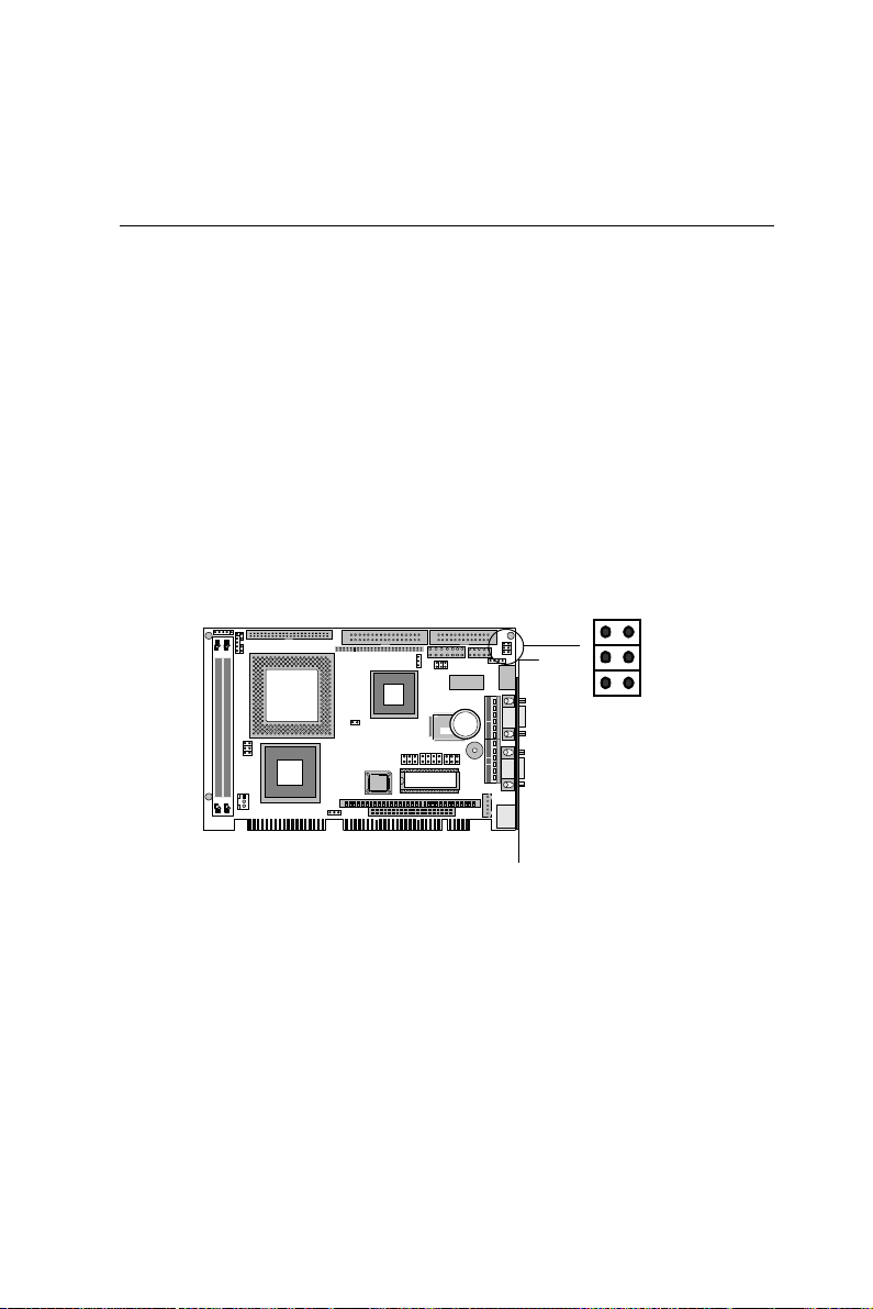
Fan power connector (CN6)
The SBC-556 onboard offer +12V voltage for the CPU cooler fan
used.
CHIPS
B69000
1
2
3
Fan power connector (CN6)
Pin Signal
1 Speed Detect
2 +12V
3 GND
SIS
5582
DiskOnChip
BAT
Winbond
34 SBC-556 User Manual
Page 43
Floppy drive connector (CN7)
You can attach up to two floppy disks to the SBC-556 onboard
controller. You can use any combination of 5¼” (360 KB and 1.2
MB) and/or 3½” (720 KB, 1.44 MB, and 2.88 MB) drives.
A 34-pin daisy-chain drive connector cable is required for a dualdrive system. On one end of the cable is a 34-pin flat-cable connector. On the other end are two sets of floppy disk drive connectors.
Each set consists of a 34-pin flat-cable connector (usually used for
3½” drives) and a printed-circuit board connector (usually used for
5¼” drives).
33 1
34 2
CHIPS
B69000
BAT
Winbond
5582
SIS
DiskOnChip
Connecting the floppy drive
1. Plug the 34-pin flat-cable connector into CN7. Make sure that the
red wire corresponds to pin 1 on the connector.
2. Attach the appropriate connector on the other end of the cable
to the floppy drive(s). You can use only one connector in the set.
The set on the end (after the twist in the cable) connects to the
A: drive. The set in the middle connects to the B: drive.
3. If you are connecting a 5¼” floppy drive, line up the slot in the
printed circuit board with the blocked-off part of the cable
connector.
Chapter 2 Installation 35
Page 44

If you are connecting a 3½” floppy drive, you may have trouble
determining which pin is pin number 1. Look for a number printed
on the circuit board indicating pin number 1. Also, the connector
on the floppy drive connector may have a slot. When the slot is
up, pin number 1 should be on the right. Check the documentation
that came with the drive for more informa-tion.
If you desire, connect the B: drive to the connectors in the middle
of the cable as described above.
Pin assignments
The following table lists the pin assignments for the CN7 connector:
FLOPPY drive connector (CN7)
Pin Signal Pin Signal
1~33 (odd) GND 2 High density
4, 6 Unused 8 Index
10 Motor enable A 12 Driver select B
14 Driver select A 16 Motor enable B
18 Direction 20 Step pulse
22 Write data 24 Write enable
26 Track 0 28 Write protect
30 Read data 32 Select head
34 Disk change
36 SBC-556 User Manual
Page 45
Parallel (Printer) port connector (CN8)
Normally, the parallel port CN8 is used to connect the card to a
printer. You need an adapter cable if you use a traditional DB-25
connector. The cable has a 26-pin connector on one end and a DB25 connector on the other.
25
1
SIS
26
CHIPS
B69000
BAT
Winbond
5582
DiskOnChip
2
Parallel port IRQ
The SBC-556 supports one parallel port. The port is designated as
LPT1 and can be disabled or changed to LPT2 or LPT3 in the system
BIOS setup.
Pin assignments
Parallel (printer) Connector (CN8)
Pin Signal Pin Signal
1 Strobe 2 Data 0
3 Data 1 4 Data 2
5 Data 3 6 Data 4
7 Data 5 8 Data 6
9 Data 7 10 -Acknowledge
11 Busy 12 Paper empty
13 +Select 14 -Auto feed
15 -Error 1 6 -Init printer
17 -Select input 18~25 GND
Chapter 2 Installation 37
Page 46
Display connectors (CN9, CN15)
The SBC-556’s PCI SVGA interface can drive conventional CR T
displays and is capable of driving a wide range of flat panel
displays, including electroluminescent (EL), gas plasma, passive
LCD and active LCD displays. The card has two connectors to
support these displays, one for standard CRT VGA monitors(CN15)
and one for flat panel displays(CN9).
The SBC-556’s SVGA connector (CN15) with PCI bus supports
monochrome display as well as high-resolution color displays. The
card also features a LCD connector (CN9), which allows you to
connect various flat panel displays. The following table lists pin
assignments of CN9:
CN9
49
50
SIS
1
2
CHIPS
B69000
BAT
Winbond
5582
DiskOnChip
CN15
38 SBC-556 User Manual
Page 47

LCD connector (CN9)
Pin Function Pin Function
1 +12VDC 2 +12VDC
3 GND 4 GND
5 +5VDC 6 +5VDC
7 ENAVEE 8 G ND
9P0 10P1
11 P2 12 P3
13 P4 14 P5
15 P6 16 P7
17 P8 18 P9
19 P10 20 P11
21 P12 22 P13
23 P14 24 P15
25 P16 26 P17
27 P18 28 P19
29 P20 30 P21
31 P22 32 P23
33 P24 34 P25
35 SHFCLK 36 FLM (V SYS)
37 M 38 LP (H SYS)
39 GND 40 ENABKL
41 P26 42 P27
43 P28 44 P29
45 P30 46 P31
47 P32 48 P33
49 P34 50 P35
Chapter 2 Installation 39
Page 48

SVGA connector (CN15)
Pin Signal
1 Red video
2 Green video
3 Blue video
4 Not used
5 GND
6 Red return (GND)
7 Green return (GND)
8 Blue return (GND)
9 Key (no pin)
10 Sync return (GND)
11 Monitor ID (not used)
12 Monitor ID
13 Horizontal sync
14 Vertical sync
15 Not used
40 SBC-556 User Manual
Page 49
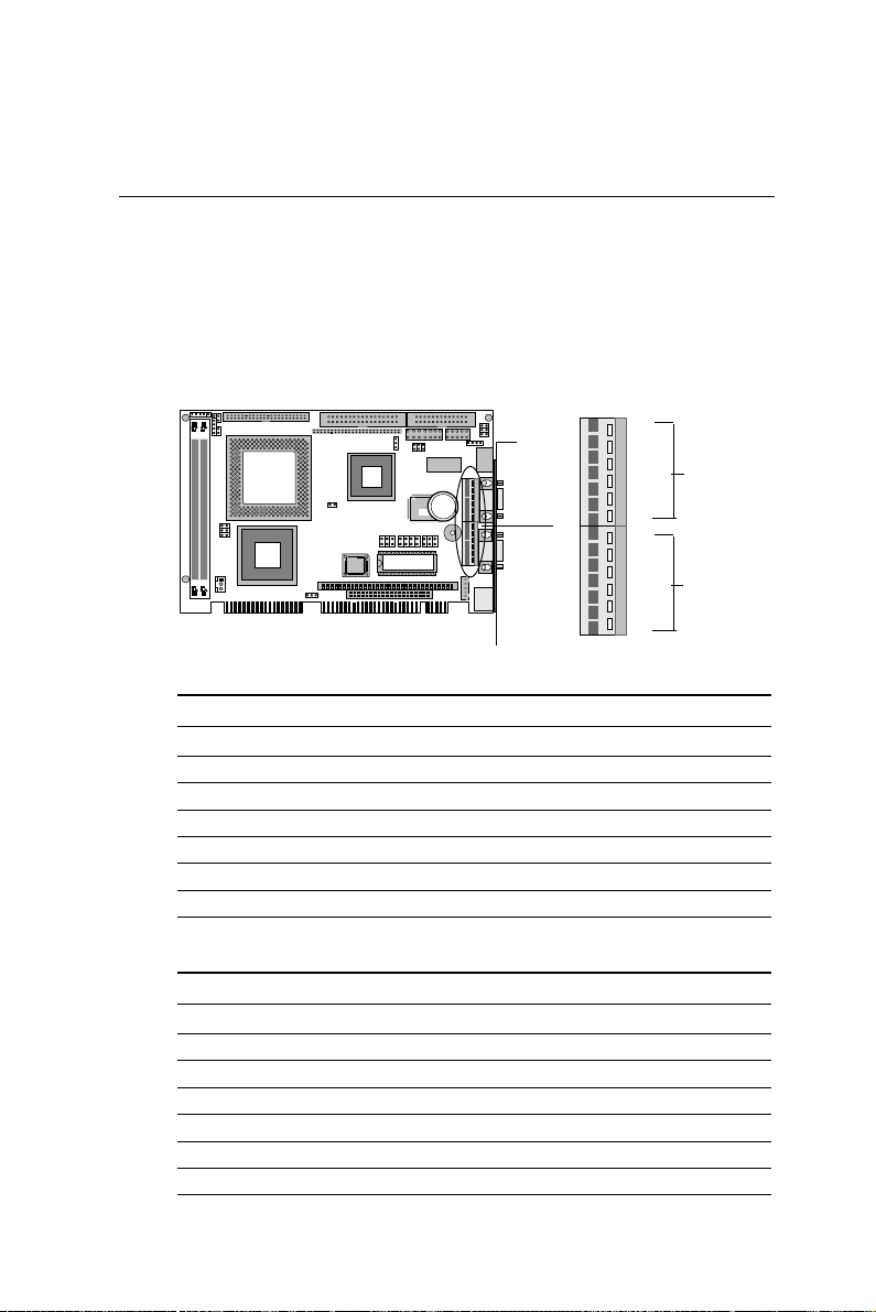
Serial ports connectors (CN10, CN14)
The SBC-556 offers one RE-232 serial port and one selectable RS232/422/485 serial ports. Y ou can enable or disable the address for
each port within the BIOS Peripheral Setup Menu.
The card mounting bracket holds COM1(CN14), the DB-9 serial
port connector for the first port For COM2(CN10) selection, please
refer to Jumper settings one the previous page.
13
1
(COM2/CN10)
SIS
14
CHIPS
B69000
5582
DiskOnChip
BAT
2
Winbond
(COM1/CN14)
niP232-SR584/224-SRniP232-SR584/224-SR
1DCDDCD2RSDRSD
3XRXR4STRSTR
5XTXT6STCSTC
7RTDRTD8IRIR
9DNGDNG01C.NC.N
11C.N
+DXT224
)+ATAD584(
21C.N
-DXT224
)-ATAD584(
31C.N+DXR22441C.N-DXR224
Chapter 2 Installation 41
Page 50
USB connectors (dual-port) (CN11)
The USB connector supports two universal serial ports. This
connector allows optional external port bracket and attached cable
to connect external USB devices. If the USB ports are installed, the
USB setting in the CMOS setup should be set to “Enabled”. The
USB ports also require operating system support for USB devices.
1
2
SIS
9
CHIPS
B69000
BAT
Winbond
5582
DiskOnChip
rotcennoCBSUrotcennoCBSU
rotcennoCBSUrotcennoCBSU
rotcennoCBSU
10
noitcnuFniP
12 V5+
34 ataD56 ataD+
78 DNG
901CN
42 SBC-556 User Manual
Page 51
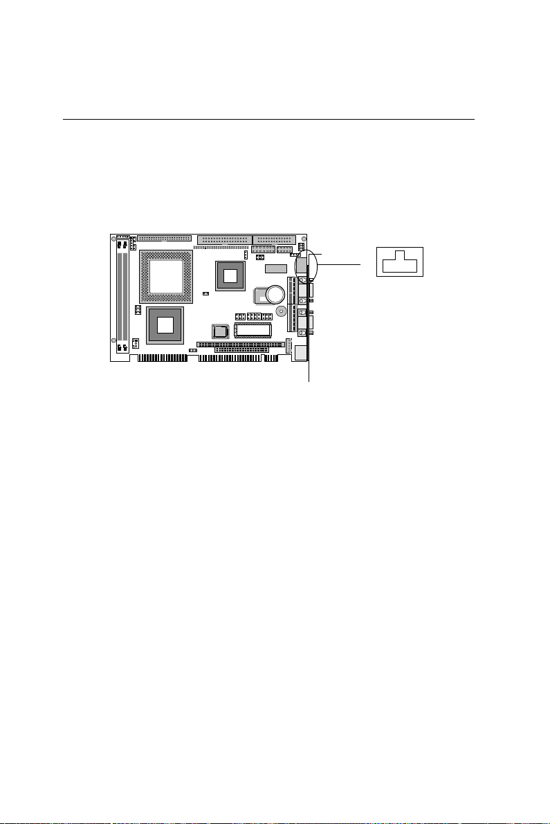
Ethernet connector (CN12)
The Ethernet interface on the SBC-556 via an standard RJ-45
connector for 100/10 Base-T operation.
CHIPS
B69000
BAT
Winbond
5582
SIS
DiskOnChip
Chapter 2 Installation 43
Page 52
Power connectors (P8 & P9)(CN13)
In single board computer (non-passive backplane) application. You
will need to connect the power directly to the SBC-556 board using
CN13. This connector is fully compatible with the standard PC PS/2
power supply connector, P8 & P9. see the following table for its pin
assignments:
1
2
CHIPS
B69000
BAT
Winbond
5582
SIS
DiskOnChip
Power connector pin assignments (CN13)
Pin (P8) Signal Pin (P9) Signal
1 +5V 1 GND
2 +5V 2 GND
3 +5V 3 -12V
4 -5V 4 +12V
5 GND 5 +5V
6 GND 6 N.C.
3
4
5
6
1
2
3
4
5
6
P9 from standare
PS/2 power supply
P8 from standare
PS/2 power supply
Power connector pin assignments (CN13)
Pin (P8) Color Pin (P9) Color
1 Red 1 Black
2 Red 2 Black
3 Red 3 Blue
4 White 4 Yellow
5 Black 5 Red
6 Black 6 Orange
44 SBC-556 User Manual
Page 53
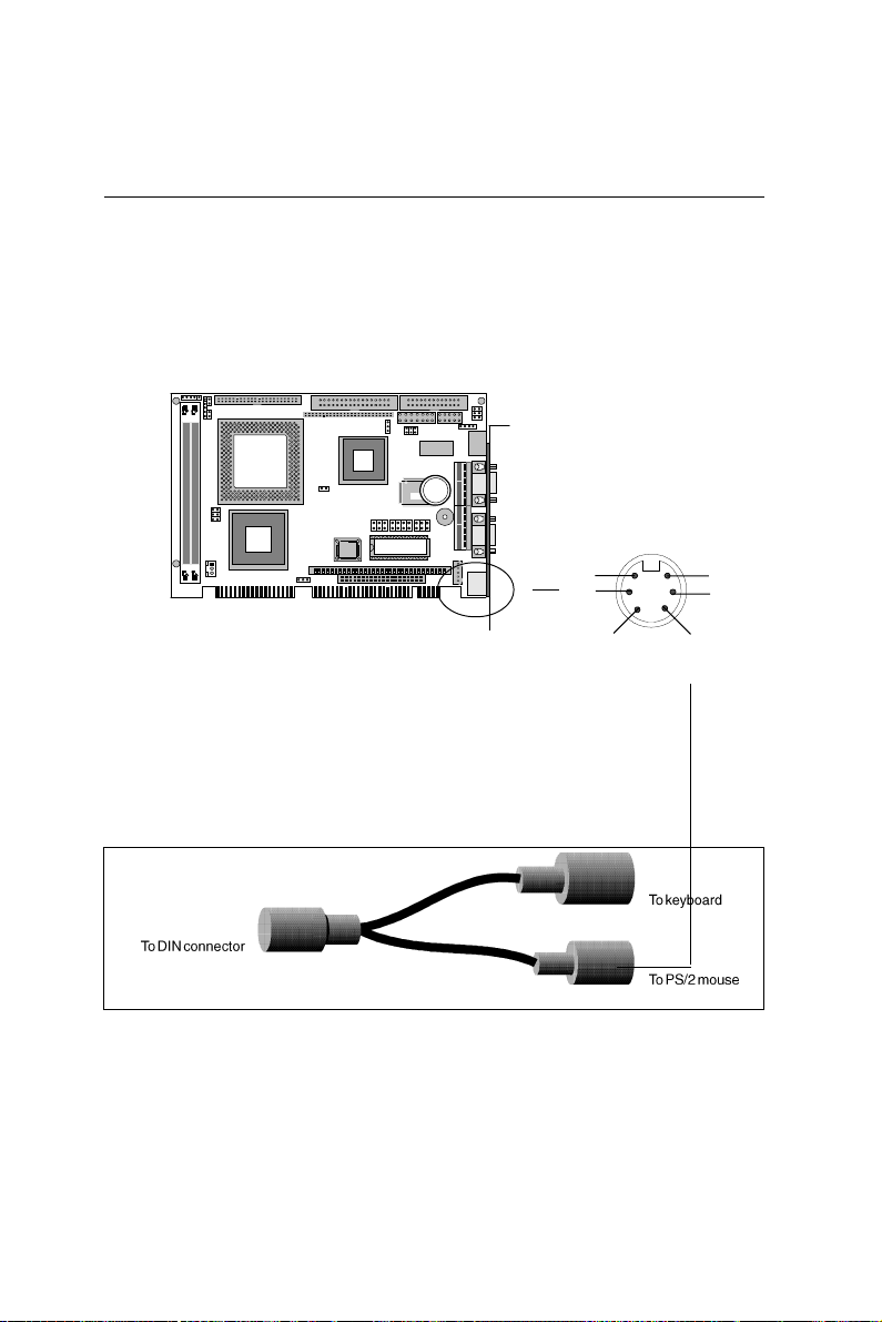
KB & PS/2 Mouse connector (CN17)
The SBC-556 board provides two 6-pin mini-DIN connectors (KB/
PS/2 MOUSE) on the card mounting bracket supports single board
computer applications. The card comes with an adapter to convert
the 6-pin mini-DIN connector, used for the mouse, to the standard
DIN connector for the keyboard.
CHIPS
B69000
BAT
Winbond
5582
SIS
DiskOnChip
6
4
5
3
KB/PS2 MOUSE
2
1
Chapter 2 Installation 45
Page 54

Keyboard connector
Pin Function
1 K.B. clock
2 K.B. data
3 N.C.
4 GND
5 +5 V DC
Keyboard & PS/2 mouse connector
Pin Function
1 K.B. data
2 PS/2 mouse data
3 GND
4 +5 V DC
5 K.B. clock
6 PS/2 mouse clock
46 SBC-556 User Manual
Page 55
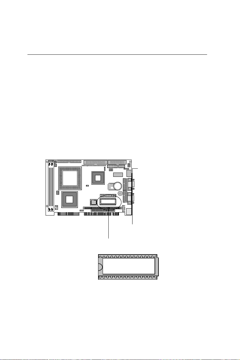
DiskOnChip socket
The DiskOnChip 2000 family of products provides a single chip
solid-state flash disk in a standard 32-pin DIP package. The
DiskOnChip 2000 is a solid-state disk with no moving parts,
resulting in a significant reduction in power consumption and an
increase in reliability. The DiskOnChip is a small, plug and play
Flash disk. It is easy to use and saves integration overhead.
The DiskOnChip 2000 family of products is available in capacities
ranging from 2MB up to 72 MB, unformatted. In order to manage
the disk, the DiskOnChip 2000 includes the TrueFFS, M-Systems'
Flash File System proprietary software. The DiskOnChip 2000
package is pin-to-pin compatible with standard 32-pin EPROM
devices.
CHIPS
B69000
BAT
Winbond
5582
SIS
DiskOnChip
16
DiskOnChip
17
1
32
Chapter 2 Installation 47
Page 56
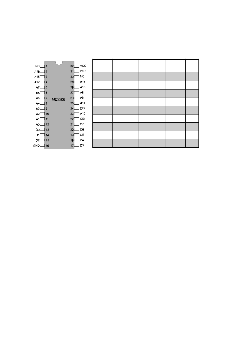
pin
Name
A0-A12 Address bus 4-12,23,25-27 Inputs
A13-A16 Address bus 2,3,28,29 Inputs 1
D0-D7 Data bus 13- 15,17-21 I/O
CE/ Chip Enable 22 Input
OE /
OE/ Output Enable 24 Input
WE/ Wr ite Enable 31 Input
NC Not connec ted 1.30 2
VCC Pow er 32
GND Ground 16
Description Pin Number Direction Note
Note 1: Pins A13 through A16 are not used
by the MD2200. They are kept for socket
backward compatibility with ED 1100
(DiskOnChip 1000)
Note 2: Pins 1 and 30 are not used by
MD2200
48 SBC-556 User Manual
Page 57

CHAPTER
3
Award BIOS Setup
This chapter describes how to set BIOS
configuration data.
Chapter 3 Award BIOS Setup 49
Page 58

System test and initialization
These routines test and initialize board hardware. If the routines
encounter an error during the tests, you will either hear a few
short beeps or see an error message on the screen. There are two
kinds of errors: fatal and non-fatal. The system can usually
continue the boot-up sequence with non-fatal errors. Non-fatal
error messages usually appear on the screen along with the
following instructions:
press <F1> to RESUME
Write down the message and press the F1 key to continue the
boot-up sequence.
System configuration verification
These routines check the current system configuration against the
values stored in the card’s CMOS memory. If they don’t match,
the program outputs an error message. You will then need to run
the BIOS setup program to set the configuration information in
memory.
There are three situations in which you will need to change the
CMOS settings:
1. You are starting your system for the first time.
2. You have changed the hardware attached to your system.
3. The CMOS memory has lost power, and the configuration
information has been erased.
The SBC-556,s CMOS memory has an integral lithium battery
backup. The battery backup should last ten years in normal
service, but when it finally runs down, you will need to replace the
complete unit.
50 SBC-556 User Manual
Page 59
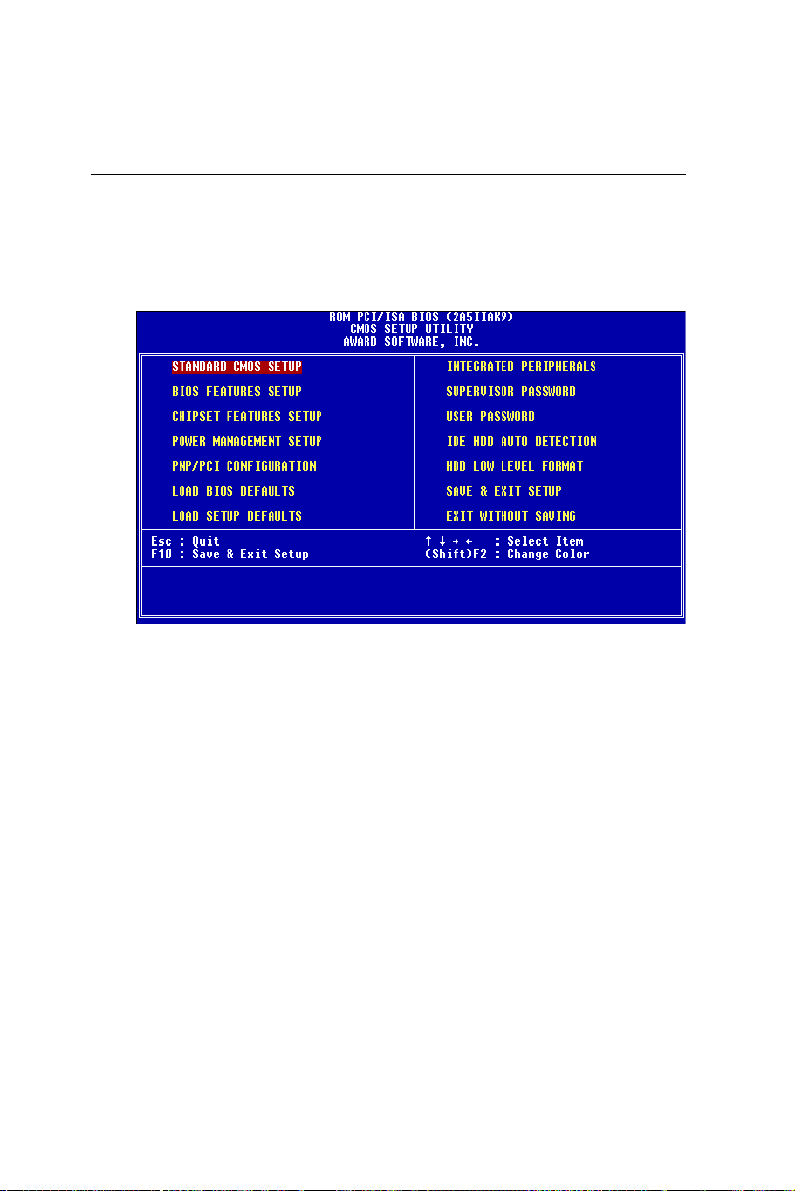
AWARD BIOS setup
Entering setup
Power up the computer and press <Del> immediately. This will
allow you to enter Setup.
Award’s BIOS ROM has a built-in Setup program that allows users
to modify the basic system configuration. This type of information is stored in battery-backed CMOS RAM so that it retains the
Setup information when the power is turned off.
Chapter 3 Award BIOS Setup 51
Page 60
Standard CMOS setup
When you choose the ST ANDARD CMOS SETUP option from the
INITIAL SETUP SCREEN menu, the screen shown below is
displayed. This standard Setup Menu allows users to configure
system components such as date, time, hard disk drive, floppy
drive, display, and memory. Once a field is highlighted, on-line
help information is displayed in the left bottom of the Menu
screen. In the Panel selection item, you can use Page/Up/Down
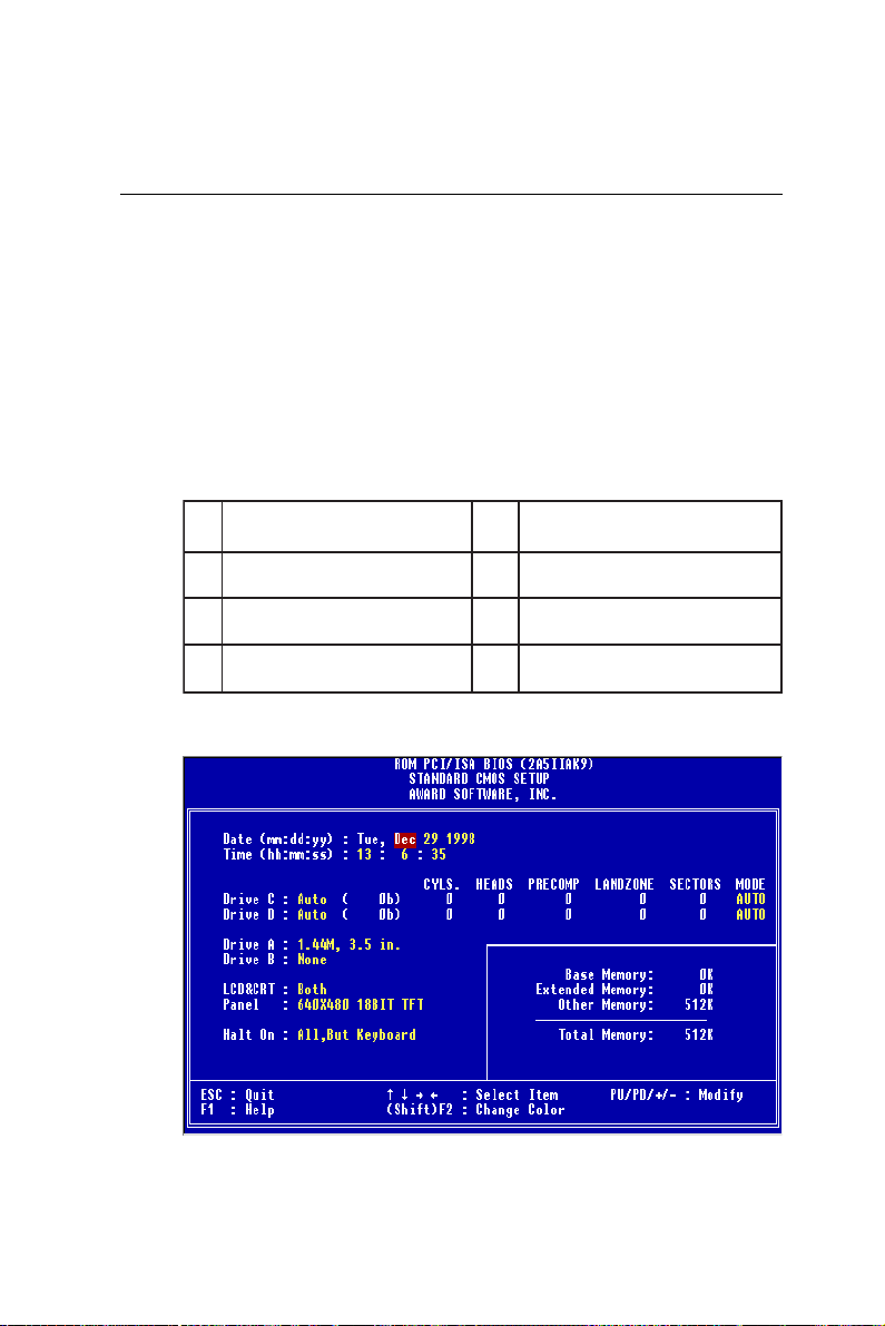
key to select requried LCD BIOS. There are eight various. LCD
BIOS available in this BIOS selection table:
11111
22222
33333
44444
TFTtiB81084x046
TFT867x4201
TFT006x008
NTSD867x4201
55555
66666
77777
88888
ONOM084x046
NTSD084x046
NTSD006x008
TFTtiB21084x046
52 SBC-556 User Manual
Page 61
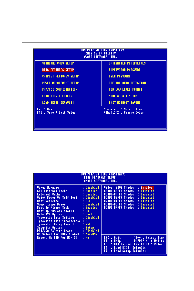
BIOS features setup
By choosing the BIOS FEATURES SETUP option from the
INITIAL SETUP SCREEN menu, the screen below is displayed.
The following configurations are based on the manufacturer's
SETUP DEF AUL TS settings.
Chapter 3 Award BIOS Setup 53
Page 62

Virus Warning
When this item is enabled, the A ward BIOS will monitor the boot
sector and partition table of the hard disk drive for any attempt at
modification. If an attempt is made, the BIOS will halt the system
and the following error message will appear. Afterwards, if
necessary, you will be able to run an anti-virus program to locate
and remove the problem before any damage is done.
! WARNING !
Disk boot sector is to be modified
T ype "Y" to accept write or "N" to abort write
Award Software, INC.
CPU Internal Cache/External Cache
These two categories speed up memory access. However, it
depends on CPU/chipset design.
Quick Power On Self Test
This category speeds up Power On Self Test (POST) after you
power up the computer. If it is set to Enable, BIOS will shorten
or skip some check items during POST.
Boot Sequence
This category determines which drive to search first for the disk
operating system (i.e., DOS).
Swap Floppy Drive
This item allows you to determine whether you want to swap
floppy drive or not.
54 SBC-556 User Manual
Page 63

Boot Up Floppy Seek
During POST, BIOS will determine if the floppy disk drive
installed is 40 or 80 tracks. 360K type is 40 tracks while 760K,
1.2 M and 1.44M are all 80 tracks.
Boot Up NumLock Status
This allows you to determine the default state of the numeric
keypad.
Gate A20 Option
This entry allows you to select how the gate A20 is handled. The
gate A20 is a device used to address memory above 1 Mbyte.
Initially, the gate A20 was handled via a pin on the keyboard.
Today, while keyboards still provide this support, it is more
common, and much faster, for the system chipset to provide
support for gate A20.
Security Option
This category allows you to limit access to the system.
Chapter 3 Award BIOS Setup 55
Page 64
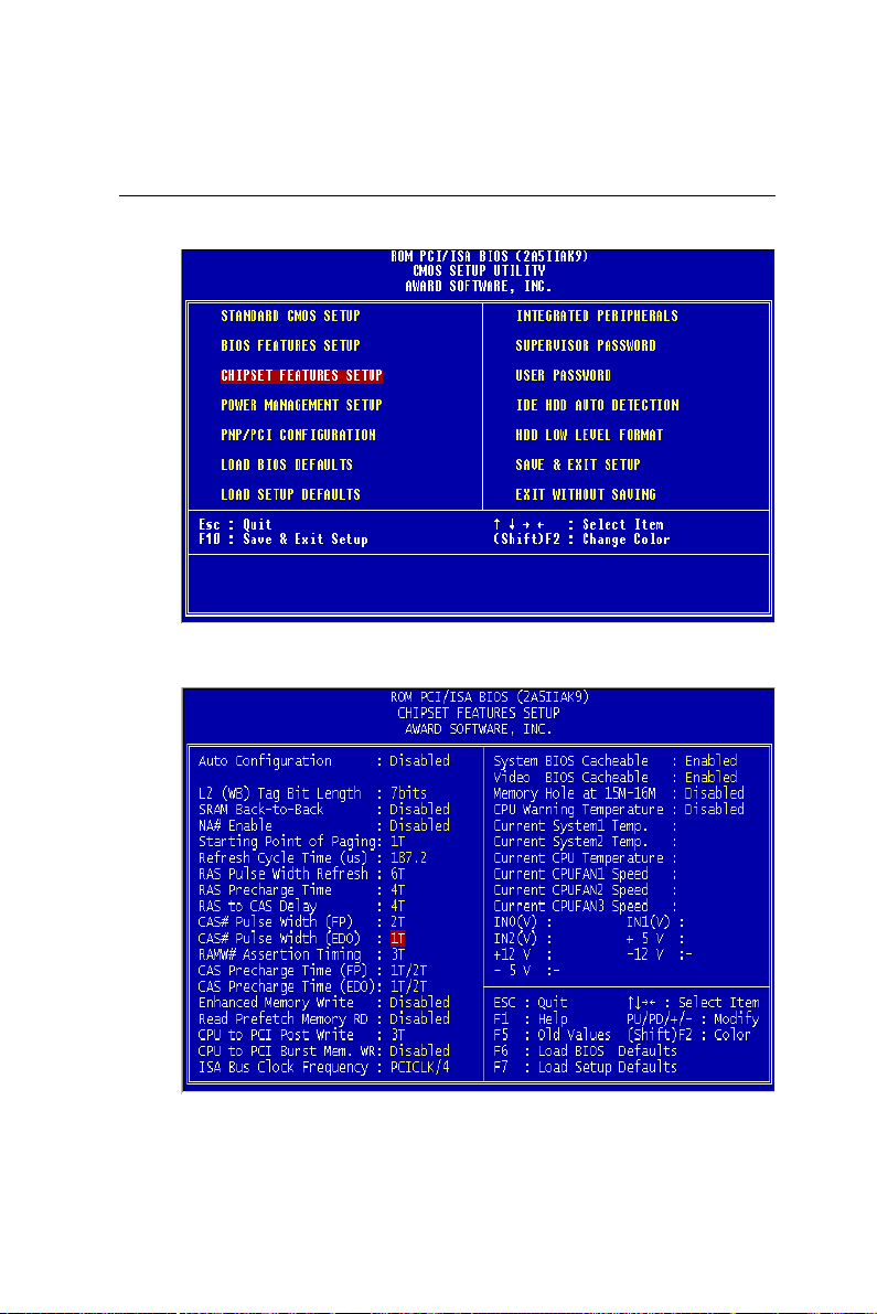
Chipset features setup
56 SBC-556 User Manual
Page 65

This section allows you to configure the system based on the
specific features of the installed chipset. This chipset manages
bus speeds and access to system memory resources, such as
DRAM and the external cache. It also coordinates communications between the conventional ISA bus and the PCI bus. It must
be stated that these items should never need to be altered. The
default settings have been chosen because they provide the best
operating conditions for your system.
The only time you might consider making any changes would be if
you discovered that data was being lost while using your system.
Auto Configuration
Set this item to Enabled to pre-defined values for DRAM,
cache.. timing according to CPU type & system clock. Thus, each
item value may display differently depending on your system
configurations.
When this item is enabled, the pre-defined items will become
SHOW-ONLY.
System BIOS Cacheable
When enabled, accesses to the system BIOS ROM addressed at
F0000H-FFFFFH are cached, provided that the cache controller
is enabled.
Video BIOS Cacheable
As with caching the System BIOS above, enabling the Video BIOS
cache will cause access to video BIOS addressed at C0000H to
C7FFFH to be cached, if the cache controller is also enabled.
Chapter 3 Award BIOS Setup 57
Page 66
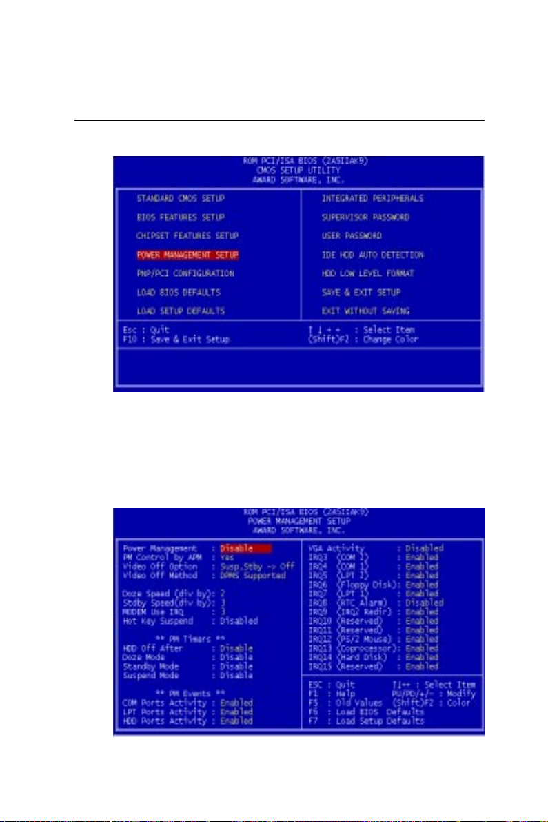
Power management setup
By choosing the POWER MANAGEMENT SETUP option from
the INITIAL SETUP SCREEN menu, the screen below is displayed. The following configurations are the setup menu on the
screen.
58 SBC-556 User Manual
Page 67

Power Management
There are four selections for Power Management, Disabled, Min
Saving, Max Saving, User Define. Except Disabled, three of
above selections have fixed mode settings. When PM is set
Disabled, the pre-defined items will become show only.
PM Control by APM
When enabled, an Advanced Power Management device will be
activated to enhance the Max. Power Saving mode and stop the
CPU internal clock.
Video Off Option
User can select All ModesàOff , Always On, SuspendàOff, or
Susp, StbyàOff to execute the PM mode.
Video Off Method
This determines the manner in which the monitor is blanked.
neercsknalB.reffubedivehtotsknalbsetirwylnonoitposihT
SMPD.gnilangistnemeganamrewopyalpsidlaitinI
Chapter 3 Award BIOS Setup 59
Page 68

PM Timers
The following four modes are Green PC power saving functions
which are only user configurable when User Defined Power
Management has been selected. See above for available selections.
HDD Off After
When enabled and after the set time of system inactivity, the hard
disk drive will be powered down while all other devices remain
active.
Doze Mode
When enabled and after the set time of system inactivity, the CPU
clock will run at a slower speed while all other devices still
operate at full speed.
Standby Mode
When enabled and after the set time of system inactivity, the fixed
disk drive and the video will be shut off while all other devices
still operate at full speed.
Suspend Mode
When enabled and after the set time of system inactivity, all
devices except the CPU will be shut off.
60 SBC-556 User Manual
Page 69

PM Events
PM events are I/O events whose occurrence can prevent the
system from entering a power-saving mode or can awaken the
system from such a mode. In effect, the system remains alert for
anything which occurs to a device which is configured as En-
abled, even when the system is in a power down mode.
The following is a list of IRQ (Interrupt ReQuests) which can be
exempted much as the COM ports and LPT ports above can.
When an I/O device wants to gain the attention of the operating
system, it signals this by causing an IRQ to occur. When the
operating system is ready to respond to the request, it interrupts
itself and performs the service.
• IRQ3 (COM 2)
• IRQ4 (COM 1)
• IRQ5 (LPT 2)
• IRQ6 (Floppy Disk)
• IRQ7 (LPT 1)
• IRQ8 (RTC Alarm)
• IRQ9 (IRQ2 Redir)
• IRQ10 (Reserved)
• IRQ1 1 (Reserved)
• IRQ12 (PS/2)
• IRQ13 (Coprocessor)
• IRQ14 (Hard Disk)
• IRQ15 (Reserved)
Chapter 3 Award BIOS Setup 61
Page 70
PNP/PCI Configuration setup
By choosing the PCI CONFIGURATION SETUP option from the
INITIAL SETUP SCREEN menu, the screen below is displayed.
This section describes configuring the PCI bus system. PCI, or
Personal Computer Interconnect, is a system which allows I/O
devices to operate at speeds nearing the speed the CPU itself uses
when communicating with its own special components. This
section covers some very technical items and it is strongly
recommended that only experienced users should make any
changes to the default settings. The following configurations are
based on the manufacturer's SETUP DEF AULTS Settings.
62 SBC-556 User Manual
Page 71
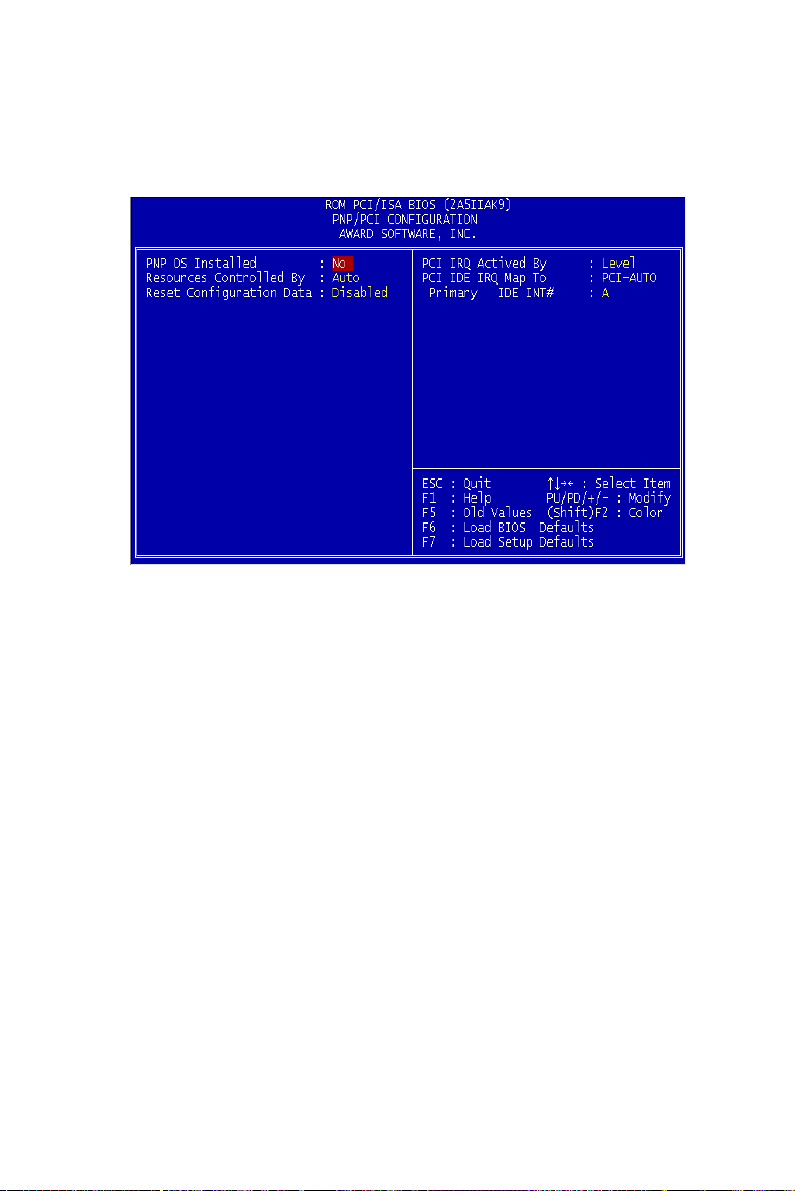
Resource Controlled by
The A ward Plug and Play BIOS has the capacity to automatically
configure all of the boot, Plug and Play compatible devices.
However, this capability means absolutely nothing unless you are
using a Plug and Play operating system such as Windows® 95
Reset Configuration data
.
This item allows you to determine whether to reset the configuration data or not.
PCI IRQ Activated by
This sets the method by which the PCI bus recognizes that an IRQ
service is being requested by a device. Under all circumstances,
you should retain the default configuration unless advised
otherwise by your system manufacturer.
Choices are Level and Edge.
Chapter 3 Award BIOS Setup 63
Page 72

PCI IDE IRQ Map to
This allows you to configure your system to the type of IDE disk
controller in use. The more apparent difference is the type of
slot being used.
If you have equipped your system with a PCI controller, changing
this allows you to specify which slot has the controller and which
PCI interrupt (A, B, C, or D) is associated with the connected
hard drives.
Remember that this setting refers to the hard disk drive itself,
rather than individual partitions. Since each IDE controller
supports two separate hard drives, you can select the INT# for
each. Again, you will note that the primary has a lower interrupt
than the secondary.
Selecting PCI Auto allows the system to automatically determine
how your IDE disk system is configured.
Primary IDE INT#
Refer to the above description of PCI IDE IRQ.
64 SBC-556 User Manual
Page 73
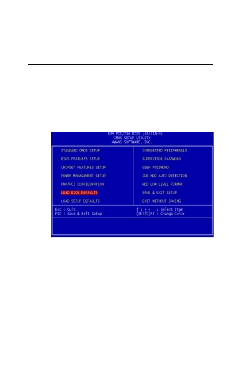
Load BIOS DEFAULTS / LOAD SETUP
DEFAULTS
LOAD BIOS DEF AULTS loads the default system values directly
from ROM. The BIOS DEF AULTS provide the most stable
settings, though they do not provide optimal performance. LOAD
SETUP DEF AULTS, on the other hand, provides for maximum
system performance. If the stored record created by the Setup
program becomes corrupted (and therefore unusable), BIOS
defaults will load automatically when you turn on the SBC-556.
Chapter 3 Award BIOS Setup 65
Page 74
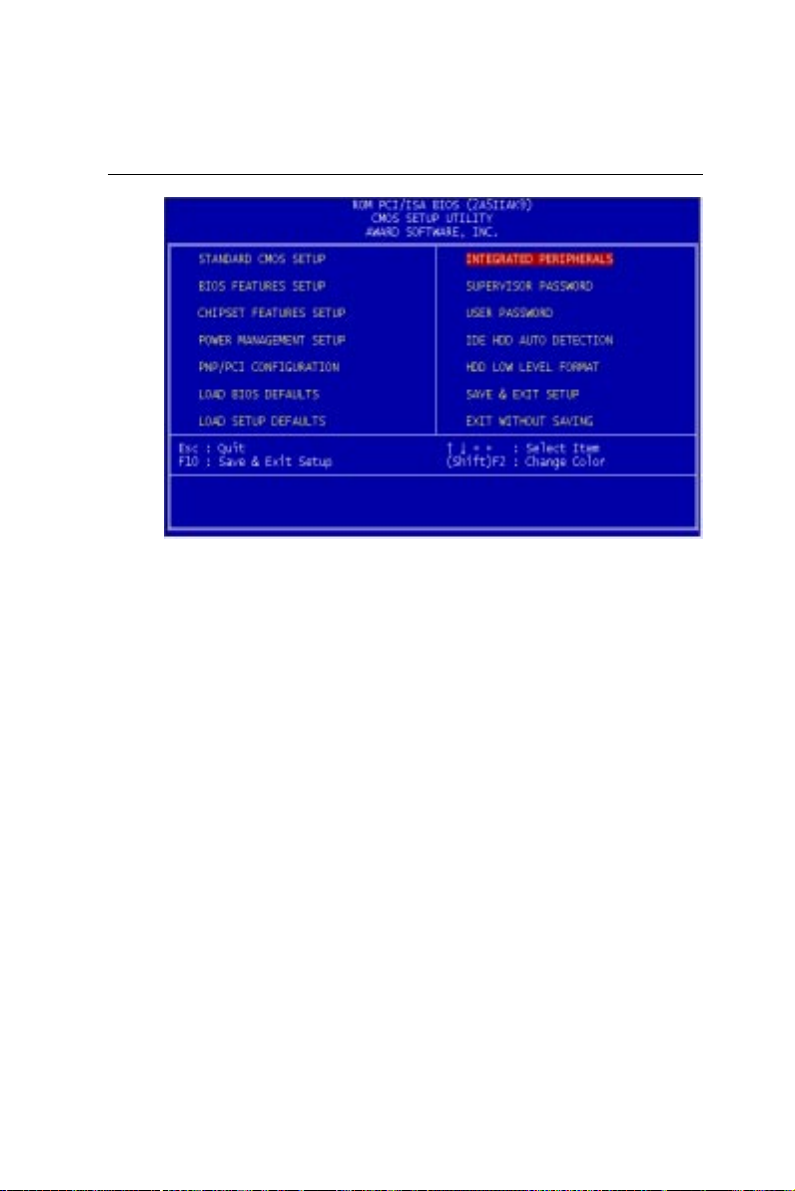
Integrated Peripherals
Integrated Peripherals options are displayed by choosing the
INTEGRA TED PERIPHERALS icon from the INITIAL SETUP
SCREEN. This section sets the IDE transfer mode for all IDE
channels. It also configures the other onboard ports. The
following configurations are based on the manufacturer's SETUP
DEF AUL TS settings.
66 SBC-556 User Manual
Page 75
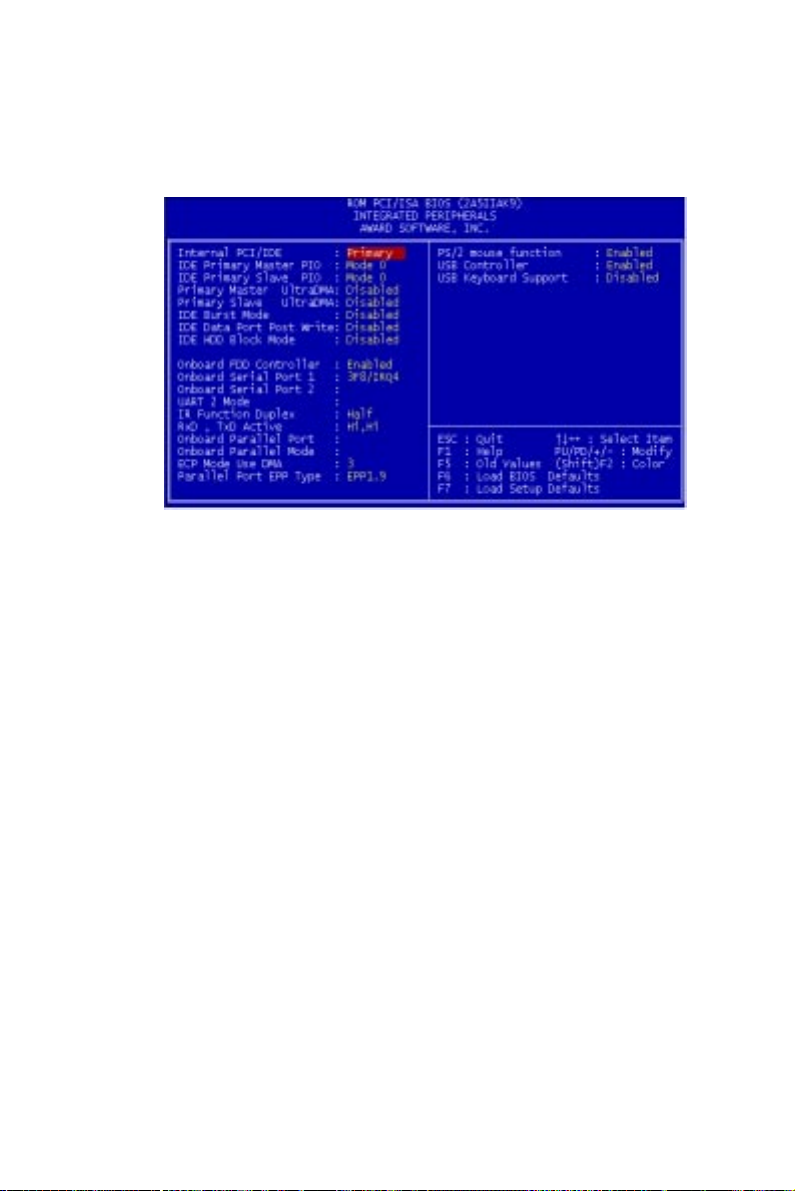
Internal PCI/IDE
You can choose Disable to terminate the onboard PCI/IDE
controller and then support external HDD devices. When the
setting is Primary, users can set up IDE Mode or UltraDMA mode
depending on the respective HDD drive.
IDE Primary Master/Slave PIO
These four lines set the hard disk PIO transfer mode, which
affects the hard disk data transfer rate. The system will autodetect the PIO mode of a device in any of these positions when
they are set to 'Auto', the recommended setting. Alternatively,
you can set the mode manually. Modes 0 to 4 are supported.
Primary Master/Slave UltraDMA
These four lines enable hard disk UltraDMA transfer mode, which
requires a drive that supports this data transfer method. The
system will auto-detect an UltraDMA device in any of these four
positions when they are set to 'Auto', the recommended setting.
The other setting is 'Disabled'. You can leave these setting on
Auto if there are no UltraDMA devices installed.
Chapter 3 Award BIOS Setup 67
Page 76

IDE Burst Mode
When this item is Enabled, the system will support burst data
transfer mode to increase HDD transfer speed.
IDE Data Port Post Write
This item allows users to select Enabled to use data port post
write for IDE drive.
IDE HDD Block Mode
Set this item to Enabled to use HDD block transfer mode.
Onboard FDD Controller
Enables or Disables the onboard Floppy Drive controllers.
Onboard Serial Port 1/2
Sets the I/O address for serial ports 1/2. The system will autodetect the COM port address when this item is set to Auto, the
default setting.
COM1/3F8 (Default of onboard serial port)
COM2/2F8 (Default of onboard serial port)
COM3/3E8
COM4/2E8
Onboard Parallel Port
Sets the I/O address for the onboard parallel port. The setting
options are:
378H/IRQ7 (default)
Disabled
278H/IRQ5
3BCH/IRQ7
68 SBC-556 User Manual
Page 77

Onboard Parallel mode
Selects the parallel port mode. The setting options are:
SPP (default)
ECP+EPP
EPP +SPP
ECP
If you set this option to 'SPP' or 'EPP', the 'ECP Mode Use DMA'
option will not appear on the screen. If you set this option to
'SPP' or 'ECP', the 'Parallel Port EPP Type' option will not appear
on the screen.
ECP Mode Use DMA
Selects the ECP Mode DMA channel. The setting options are:
3
1
USB Controller/ USB Keyboard Support
Enables or Disables the onboard USB port controller and USB
Keyboard support.
Chapter 3 Award BIOS Setup 69
Page 78
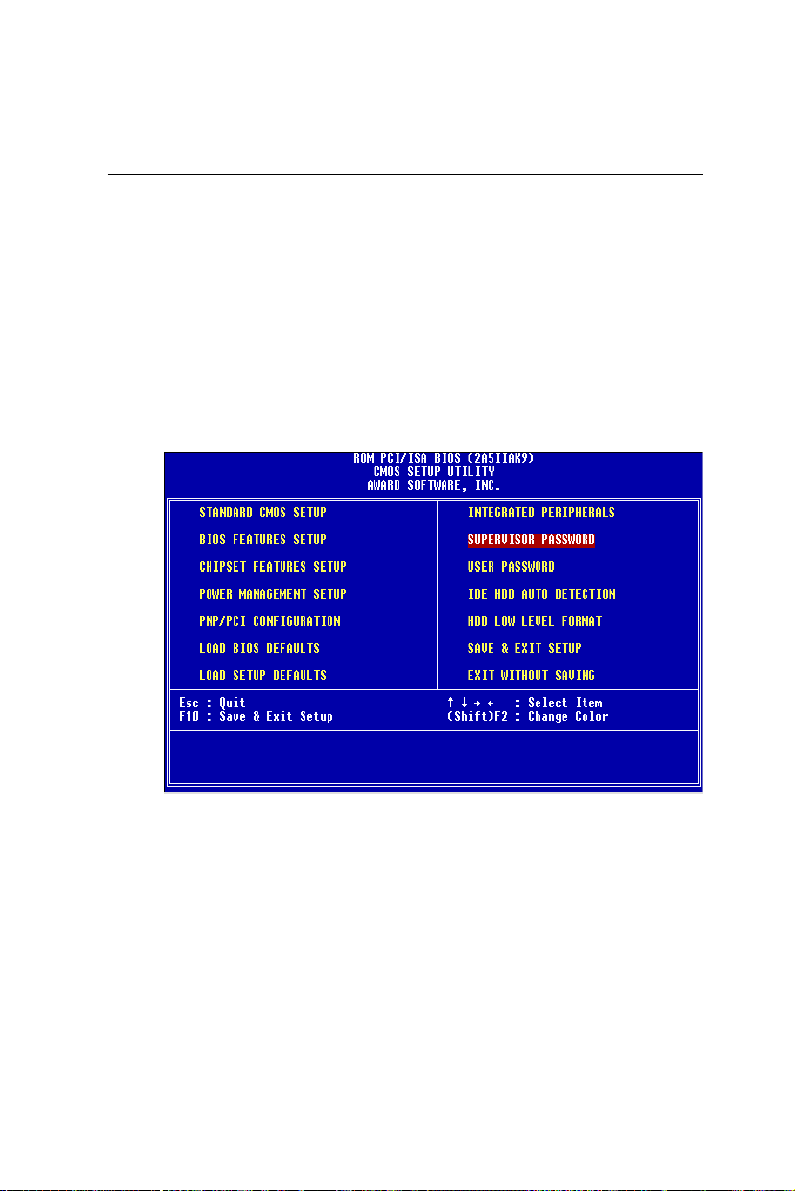
Supervisor/User Password Setting
You can set either supervisor or user password, or both. The
differences between them are:
supervisor password: can enter and change the options of
the setup menus.
user password : can only enter but does not have the right
to change the options of the setup menus.
When you select this function, the following message will appear
at the center of the screen to assist you in creating a password.
ENTER P ASSWORD:
70 SBC-556 User Manual
Page 79

ENTER P ASSWORD:
Type the password, up to eight characters in length, and press
<Enter>. The password typed now will clear any previously
entered password from the CMOS memory. You will be asked to
confirm the password. Type the password again and press
<Enter>. You may also press <Esc> to abort the selection and
not enter a password.
To disable a password, just press <Enter> when you are prompted
to enter the password. A message will confirm the password will
be disabled. Once the password is disabled, the system will boot
and you can enter Setup freely.
PASSWORD
When a password has been enabled, you will be prompted to enter
it every time you try to enter Setup. This prevents unauthorized
use of your computer.
Chapter 3 Award BIOS Setup 71
Page 80
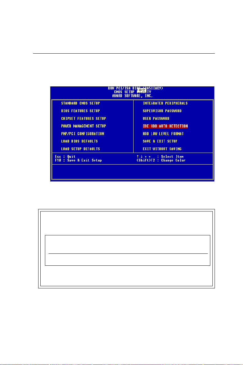
Auto detect hard disk
The IDE HDD AUTO DETECTION utility can automatically
detect the IDE hard disk installed in your system. You can use it
to self-detect and/or correct the hard disk type configuration.
R O M P C I / I S A B I O S ( 2 A 5 L 9 A K D )
C M O S S E T U P U T I L I T Y
A W A R D S O F T W A R E , I N C .
Drive C : (Mb) 790 15 35535 789 57
OPTION Size CYLS HEADS PRECOMP LANDZONE SECTORS MODE
1 (Y) 0 0 0 0 0 0 NORMAL
Notes: Some OSes (line SCO-UNIX) Must use "NORMAL" for installation
CYLS. HEADS PRECOMP LANDZONE SECTORS MODE
Select Drive C Option (N=Skip) : N
ESC = SKIP
IDE HDD auto detection screen
72 SBC-556 User Manual
Page 81
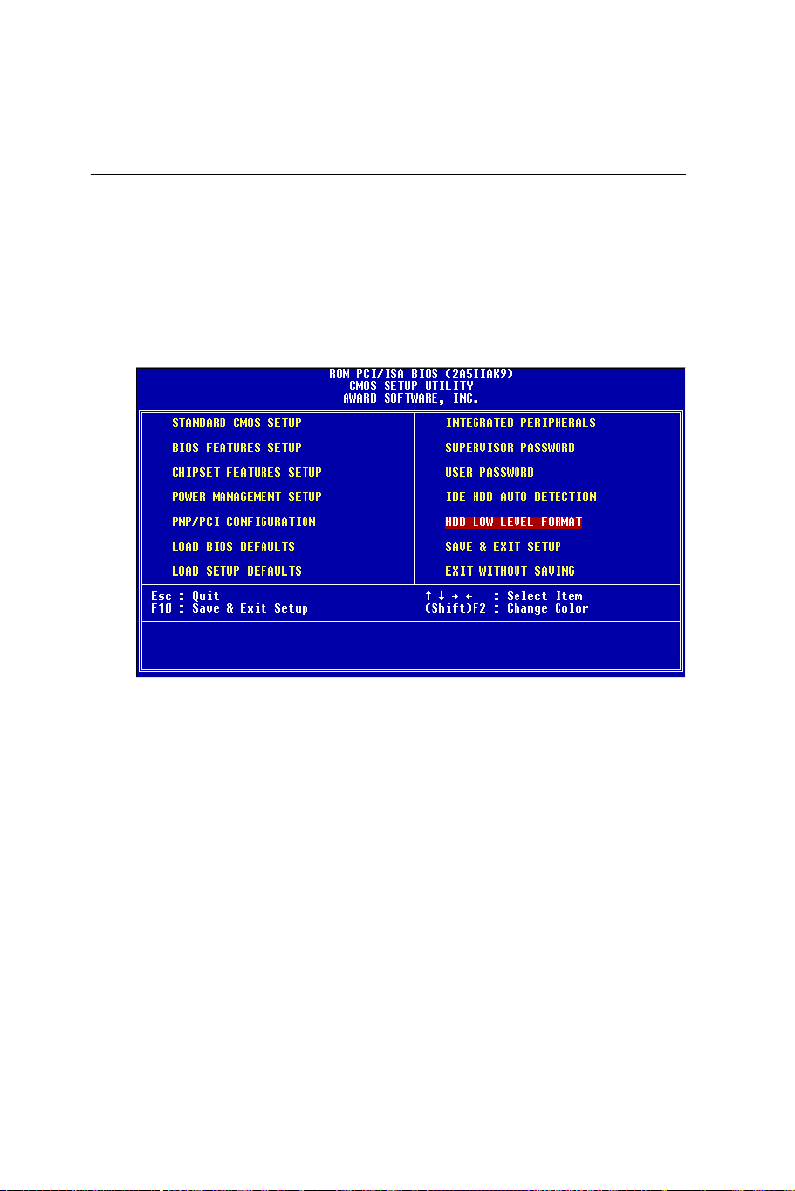
HDD low level format
Selecting this utility allows you to execute HDD low level
formatting. This Award Low-Level-Format Utility is designed as
a tool to save you time formatting your hard disk. The Utility
automatically looks for the necessary information of the drive
you selected. The Utility also searches for bad tracks and lists
them for your reference.
Shown below is the menu that appears after you enter into the
A ward Low-Level-Format Utility.
Chapter 3 Award BIOS Setup 73
Page 82
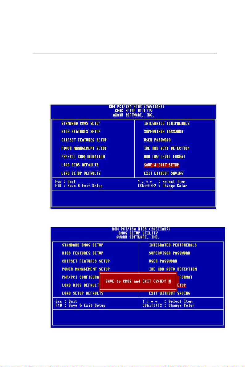
Save & exit setup
If you select this option and press <Enter>, the values entered in
the setup utilities will be recorded in the chipset's CMOS
memory. The microprocessor will check this every time you turn
on your system on and compare this to what it finds as it checks
the system. This record is required for the system to operate.
74 SBC-556 User Manual
Page 83
Exit without saving
Selecting this option and pressing <Enter> lets you exit the Setup
program without recording any new values or changing old ones.
Chapter 3 Award BIOS Setup 75
Page 84

76 SBC-556 User Manual
Page 85

4
CHAPTER
Flat Panel/CRT
Controller Display
Drivers and Utilities
This chapter provides information about:
• Driver types and installation
Chapter 4 Driver Installation 77
Page 86

Software drivers
This chapter describes the operation and installation of the display
drivers supplied on the Supporting CD-ROM that are shipped with
your product.
The onboard VGA adapter is based on the CHIPS VGA Flat Panel/CRT
controller and is fully IBM VGA compatible. This controller offers a
large set of extended functions and higher resolutions. If you intend to
use your VGA adapter in standard VGA modes only, you do not need
to install any of these drivers. Since your VGA adapter is fully compatible, it does not require any special drivers to operate in standard
modes.
The purpose of the enclosed software drivers is to take advantage of
the extended features of the CHIPS VGA Flat Panel/CRT controller.
Hardware configuration
Some of the high-resolution drivers provided in this package will
work only in certain system configurations. If a driver does not
display correctly, try the following:
1. Change the display controller to CRT-only mode, rather than flat
panel or simultaneous display mode. Some high-resolution
drivers will display correctly only in CRT mode.
2. If a high-resolution mode is not supported on your system, try
using a lower-resolution mode. For example, 1024 x 768 mode
will not work on some systems, but 800 x 600 mode is supported
on most.
78 SBC-556 User Manual
Page 87

Necessary prerequisites
The instructions in this manual assume that you understand elementary concepts of MS-DOS and the IBM Personal Computer. Before you
attempt to install any driver from the Supporting CD-ROM, you
should:
• Know how to copy files from a CD-ROM to a directory on the hard
disk
• Understand the MS-DOS directory structure
If you are uncertain about any of these concepts, please refer to the
DOS or OS/2 user reference guides for more information before you
proceed with the installation.
Before you begin
Make sure you know the version of the application for which you are
installing drivers. The Supporting CD-ROM contain drivers for several
versions of certain applications. For your driver to operate properly ,
you must install the driver for your version of the application program.
Chapter 4 Driver Installation 79
Page 88
Windows® 95
These drivers are designed to work with MicrosoftÒ WindowsÒ. You
just install these drivers through the WindowsÒ operating system.
Driver installation
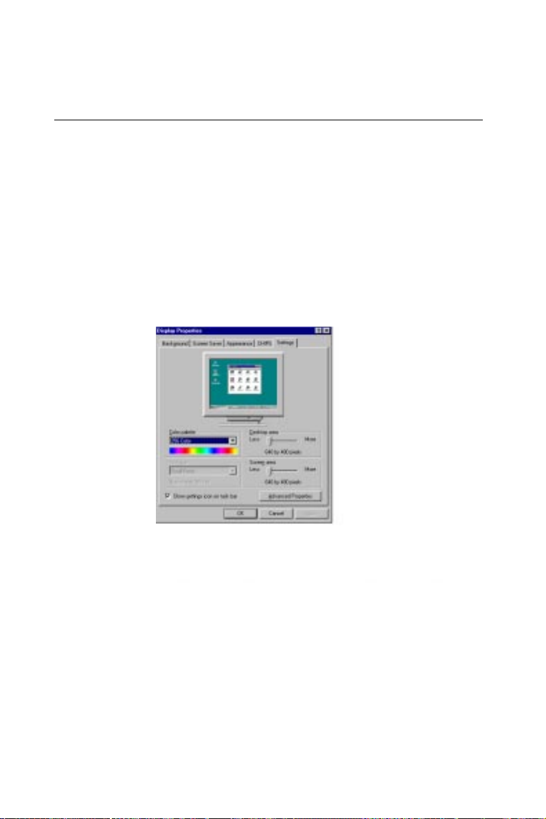
1. Install W indowsÒ 95 as you normally would for a VGA display .
Click the Start button, go to Settings and click on Control
Panel. Choose the Display icon and double click on the icon.
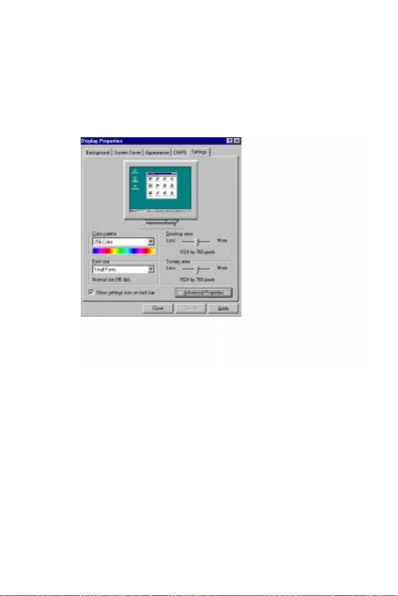
In the Display Properties window, show as figure 1:
80 SBC-556 User Manual
figure 1
Page 89
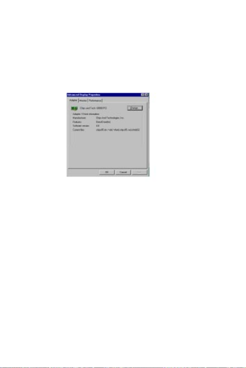
Click the setting buttom, then click the Advanced Properties icon
into the Advanced Display properties windows, show as figure2:
figure 2
Chapter 4 Driver Installation 81
Page 90
click on Change Display T ype. In the Change Display Type
window, click on the Change button under Adapter Type into the
select Device window show as figure 3: This will bring up the
Select Device window.
figure 3
82 SBC-556 User Manual
Page 91
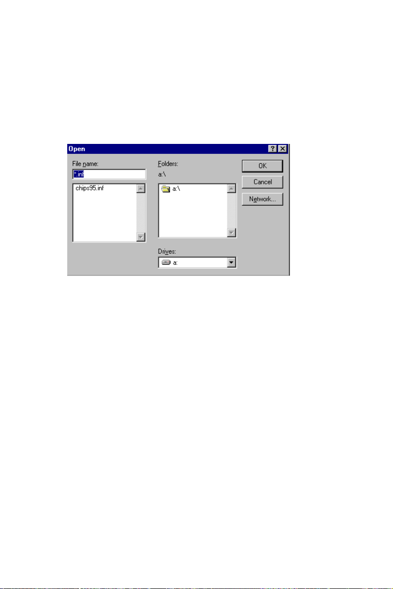
2 . Place the Supporting CD-ROM in your CD-ROM drive.
figure 4
In the Select Device window , click on Have Disk, Select Browse,
and find the Win95 driver "chips95.inf" in the Supporting CD-
ROM:
cd-rom: \CD ROM\model name\driver\vga driver
\win95\chips95.inf and then click OK.
"cd-rom" : the drive letter of your CD-ROM drive
"model name" : the model number of your product
Chapter 4 Driver Installation 83
Page 92
The name of the Chips And T ech "69000 PCI " driver will appear
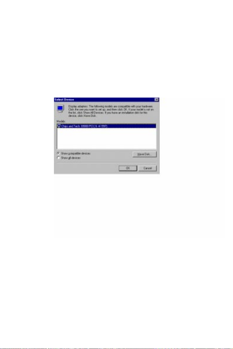
highlighted in the Models list boxfhow as figure. Click OK to start
the driver installation show as figure 5:
figure 5
84 SBC-556 User Manual
Page 93
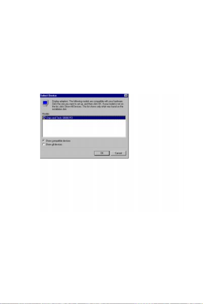
3. Once the installation is complete, the Advanced display Properties
window will reappear. Show as figure 6:
figure 6
Chapter 4 Driver Installation 85
Page 94
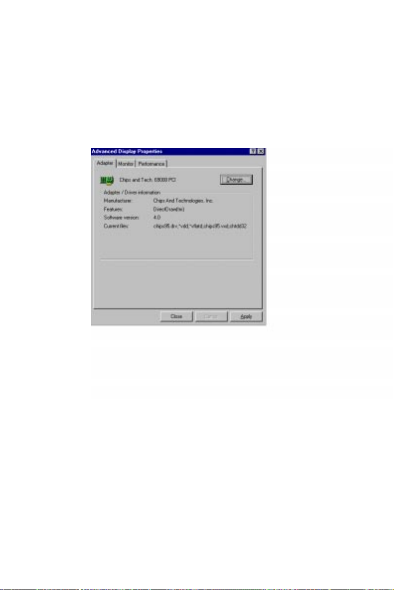
Click on close to close the window. Then the Display Properties
window
will
reappear.
S h o w
as
figure
7:
figure 7
86 SBC-556 User Manual
Page 95

Click
on
Apply.
Restart
the
system
for
the
new
settings
to
take
effect, show as figure 8:
figure 8
Chapter 4 Driver Installation 87
Page 96

Windows® 3.1
These drivers are designed to work with Microsoft Windows Version
3.1. You should install these drivers through Windows.
Driver installation
1. Install W indows as you normally would for a VGA display. Run
Windows to make sure that it is working correctly.
2 . Place the Supporting CD-ROM into your CD-ROM drive. In
Windows Program Manager, choose File from the Options Menu.
Then from the pull-down menu, choose Run. At the Command Line
prompt, type.
cd-rom:\CD ROM\model name\driver\vga driver\win31\setup.exe
Press the <ENTER> key or click OK to begin the installation.
"cd-rom" : the drive letter of your CD-ROM drive
"model name" : the model number of your product
At this point the setup program locates the directory where Windows
is installed. For proper operation, the drivers must be installed in the
Windows subdirectory.
3 . Press <ENTER> to complete the installation. Once completed, you
can find the icon Chips CPL under the Control Panel. The icon
allows you to select and load the installed drivers.
88 SBC-556 User Manual
Page 97

OS/2
These drivers are designed to function with the OS/2 V ersion 4.0, 3.0
and 2.11 operating systems.
T o install this driver , do the following steps:
1 . Open an OS/2 full screen or windowed session.
2 . Place the Supporting CD-ROM into your CD-ROM drive.
3 . At the OS/2 command prompt, type the following commands to
copy the files to the OS/2 drive:
T ype cd-rom drive:\CD ROM\model name\driver\vga driver\os2\
When the Setup Program is completed, you will need to perform a
shutdown and then restart the system in order for changes to take
effect.
"cd-rom" : the drive letter of your CD-ROM drive
"model name" : the model number of your product
A log of the information output during the install can be found
in <root>:\OS2\INST ALL\DISPLA Y .LOG
4 . After restarting the system, perform the following steps:
1. Open the OS/2 System folder.
2. Open the System Setup folder.
3. Open the Display Driver Install Object.
This step will execute the Display Driver Installation (DSPINSTL)
utility program to finish installation of the new drivers.
4. When the Display Driver Install window appears, select
Primary Display and then select OK.
5. When the Primary Display Driver List window appears, select
"Chips and T echnologies 69000" from the list of adapter types,
then select OK or install the video driver.
Chapter 4 Driver Installation 89
Page 98

6. When the installation is complete, you will need to shut down
and then restart the system for the changes to take effect.
Make sure to remove the installation diskette before restarting
the system.
90 SBC-556 User Manual
Page 99

Windows® NT 3.51
These drivers are designed to work with MicrosoftÒ WindowsÒ.
Driver installation
1. Install WindowsÒ NT 3.51 as you normally would for a VGA
display. Click the Star buttom, go to Settings and click on Control
Panel icon. Then choose the Display and double click on the icon.
In the Display Properties window , click the Setting buttom, then
click the Display T ype buttom into the Display T ype windows, then
click on Change buttom from the Adapter T ype icon. And click on
Have Disk buttom in the change display window .
2. Place the Supporting CD-ROM into your CD-ROM drive.
and type:
cd-rom: \CD ROM\model name\drive\vga drive\
win98 nt\windows.nt\nt35\Oemsetup.inf
"cd-rom" : the drive letter of your CD-ROM drive
"model name" : the model number of your product
Select the adapter "Chips and T ech 69000PCI" and click OK.
Click on Install to install the selected driver. Once the installation is
complete, shut down and restart the system.
Chapter 4 Driver Installation 91
Page 100

Windows® NT 4.0
Driver installation
1. Install WindowsÒ NT 4.0 as you normally would for a VGA
display. Click the Star buttom, go to Settings and click on Control
Panel icon. Then choose the Display and double click on the icon.
In the Display Properties window , click the Setting buttom, then
click the Display T ype buttom into the Display T ype windows, then
click on Change buttom from the Adapter T ype icon. And click on
Have Disk buttom in the change display window .
2. Place the Supporting CD-ROM into your CD-ROM dirve. In the
Select Device window, click on Have Disk, select "Browse" and
find the NT 4.0 driver from:
cd-rom : \CD ROM\model name\dirver\vga driver\
win98 nt\windows.nt\nt40\Oemsetup.inf
"cd-rom" : the drive letter of your CD-ROM drive
"model name" : the model number of your product
and then click OK. The name of the Chips and T echnologies, Inc.
Video Controller driver will appear highlighted in the Modules list
box. Select Chips and Tech. 69000 and Click OK . Click OK to start
the driver installation.
3. Once the installation is complete, the Change Display Type window
will reappear. Click on close to close the window. Then the
Display Properties window will reappear. Click on Apply. Restart
the system for the new settings to take effect.
92 SBC-556 User Manual
 Loading...