

Page 1
PC/104 Module PFM-CVS
PFM-CVS
Intel® Atom™ N2600 Processor
DDR3 1066 SODIMM
18-bit Single Channel LVDS LCD
4 USB2.0, 4 COM, 1 SATA, 1 mSATA
1 Gigabit Ethernet, PC/104+
Mini Card (Optional)
PFM-CVS Manual Rev. A 2nd Ed.
December 2012
Page 2

PC/104 Module PFM-CVS
Copyright Notice
This document is copyrighted, 2012. All rights are reserved. The
original manufacturer reserves the right to make improvements to the
products described in this manual at any time without notice.
No part of this manual may be reproduced, copied, translated, or
transmitted in any form or by any means without the prior written
permission of the original manufacturer. Information provided in this
manual is intended to be accurate and reliable. However, the original
manufacturer assumes no responsibility for its use, or for any infringements upon the rights of third parties that may result from its
use.
The material in this document is for product information only and is
subject to change without notice. While reasonable efforts have been
made in the preparation of this document to assure its accuracy,
AAEON assumes no liabilities resulting from errors or omissions in
this document, or from the use of the information contained herein.
AAEON reserves the right to make changes in the product design
without notice to its users.
i
Page 3

PC/104 Module PFM-CVS
Acknowledgments
All other products’ name or trademarks are properties of their
respective owners.
®
Intel
Microsoft Windows
ITE is a trademark of Integrated Technology Express, Inc.
IBM, PC/AT, PS/2, and VGA are trademarks of International
All other product names or trademarks are properties of their
respective owners.
and Atom are trademarks of Intel® Corporation.
®
is a registered trademark of Microsoft Corp.
Business Machines Corporation.
ii
Page 4

PC/104 Module PFM-CVS
Packing List
Before you begin installing your card, please make sure that the
following materials have been shipped:
Jumper Cap
Product CD
PFM-CVS with Heatsink
If any of these items are missing or damaged, please contact your
distributor or sales representative immediately.
iii
Page 5

PC/104 Module PFM-CVS
Contents
Chapter 1 General Information
1.1 Introduction................................................................... 1-2
1.2 Features....................................................................... 1-3
1.3 Specifications............................................................... 1-4
Chapter 2 Quick Installation Guide
2.1 Safety Precautions....................................................... 2-2
2.2 Location of Connectors and Jumpers .......................... 2-3
2.3 Mechanical Drawing..................................................... 2-5
2.4 List of Jumpers............................................................. 2-7
2.5 List of Connectors ........................................................ 2-8
2.6 Setting Jumpers ......................................................... 2-10
2.7 LVDS Voltage Selection (JP2)................................... 2-11
2.8 AT/ATX Selection and LVDS Backlight Control Voltage
Selection (JP3)................................................................. 2-11
2.9 COM2 +5V/Ring/+12V Selection (JP6)...................... 2-12
2.10 PCI-104 VIO Voltage Selection (JP7)...................... 2-12
2.11 Clear CMOS (JP8) ................................................... 2-12
2.12 PC/104 -5V/-12V Voltage Selection (JP11) Reserved
.......................................................................................... 2-13
2.13 Backlight Brightness Control Connector (CN2)........ 2-13
2.14 Internal LVDS Connector (CN3)............................... 2-14
2.15 SATA Power Connector (CN5) ................................ 2-15
iv
Page 6

PC/104 Module PFM-CVS
2.16 PCI-104 Connector (CN6)........................................ 2-15
2.17 Front Panel Connector (CN7) .................................. 2-15
2.18 +12VSB Power Input Connector (CN9) ................... 2-16
2.19 PC/104/ ISA Connector (CN11)............................... 2-16
2.20 Digital I/O Connector (CN12)................................... 2-17
2.21 Mini PCI Express/mSATA Connector (CN14) (Optional)
.......................................................................................... 2-17
2.22 Battery Connector (BT1).......................................... 2-22
2.23 SATA Connector (SATA1) ....................................... 2-23
2.24 CRT Connector (VGA1)........................................... 2-23
2.25 COM1 RS-232 Connector (COM1).......................... 2-24
2.26 COM2 RS-232/422/485 Connector (COM2)............ 2-25
2.27 COM3 RS-232 Connector (COM3).......................... 2-26
2.28 COM4 RS-232 Connector (COM4).......................... 2-27
2.29 USB2.0 Connector (USB1) ...................................... 2-28
2.30 USB2.0 Connector (USB2) ...................................... 2-28
2.31 USB2.0 Connector (USB3) ...................................... 2-29
2.32 USB2.0 Connector (USB4) ...................................... 2-29
2.33 FAN Connector (FAN1) Reserved ........................... 2-30
2.34 LAN Connector (LAN1) ............................................ 2-30
2.35 DDR3 SODIMM Connector (DIMM1)....................... 2-31
Chapter 3 AMI BIOS Setup
3.1 System Test and Initialization. ..................................... 3-2
3.2 AMI BIOS Setup........................................................... 3-3
v
Page 7

PC/104 Module PFM-CVS
Chapter 4 Driver Installation
4.1 Installation.................................................................... 4-3
Appendix A Programming The Watchdog Timer
A.1 Programming ............................................................A-2
A.2 F81866 Watchdog Timer Initial Program……………A-5
Appendix B I/O Information
B.1 I/O Address Map.......................................................B-2
st
B.2 1
MB Memory Address Map ...................................B-4
B.3 IRQ Mapping Chart...................................................B-5
B.4 DMA Channel Assignments......................................B-7
Appendix C Mating Connector
C.1 List of Mating Connectors and Cables......................C-2
Appendix D Electrical Specifications for I/O Ports
D.1 Electrical Specifications for I/O Ports .......................D-2
D.2 DIO Programming.....................................................D-3
D.3 Digital I/O Register....................................................D-4
D.4 Digital I/O Sample Program......................................D-6
vi
Page 8

PC/104 Module PFM-CVS
Chapter
1
General
Information
Chapter 1 General Information 1- 1
Page 9

PC/104 Module PFM-CVS
1.1 Introduction
AAEON Technology, a leading company in embedded boards
manufacturing with a full range of PC/104 Modules, launches a brand
new PC/104 CPU Module-PFM-CVS. Its compact size and rich
functionality ensures the most cost effective and compatible module to
coincide with your existing system planning devices.
PFM-CVS adopts an Intel
®
Atom N2600 Dual Core 1.6 GHz Processor
with the latest Intel technology. Although PFM-CVS is a small board,
it offers the full functions for customers demand. The chipset of
PFM-CVS deploys Intel
®
Atom™N2600 and NM10 that make this
board achieve high performance. It features one
10/100/1000Base-TX Ethernet port, four USB 2.0 ports, four COM
ports. In addition, the PFM-CVS equips PC/104+ socket and
Half-size mSATA/ Mini Card (optional) for flexible expansions.
Chapter 1 General Information 1- 2
Page 10

PC/104 Module PFM-CVS
1.2 Features
Fanless Intel® Atom™ N2600 Dual Core 1.6 GHz
Processor
Intel
®
Atom™ N2600 + NM10
204-pin DDR3 1066 MHz SODIMM x 1, Max. 2 GB
10/100/1000Base-TX Ethernet x 1
CRT, 18-bit Single Channel LVDS LCD
SATA 3.0 Gb/s x 1
USB2.0 x 4, COM x 4
PC/104+ Standard Form Factor Legacy ISA Support. (w/IO
Mode), mSATA / Mini Card (Optional) (Half Size support)
+12V Only Operation
Chapter 1 General Information
1 - 3
Page 11

PC/104 Module PFM-CVS
1.3 Specifications
System
Form Factor PC/104
Processor Intel
processor
System Memory DDR3 1066 MHz SODIMM x 1,
Max. 2 GB
Chipset Intel
I/O Chipset Fintech F81866D
Ethernet Realtek RTL8111E for
10/100/1000Base-TX, RJ-45 x 1
BIOS AMI BIOS – 32MB ROM
Wake on LAN Yes
®
Atom™ N2600 1.6 GHz
®
Atom™ N2600+ NM10
Watchdog Timer Generates a time-out system
reset
H/W Status Monitoring Supports power supply voltage
and temperature monitoring
Expansion Interface PC/104+, mSATA/ Mini Card(for
Half-size)
Power Requirement +12V, AT (Default) /ATX
Battery Lithium battery
Board Size 3.55” x 3.77” (90mm x 96mm)
Gross Weight 0.35 lb (0.16 Kg)
Chapter 1 General Information 1- 4
Page 12

PC/104 Module PFM-CVS
Operating Temperature 32ºF ~ 140ºF (0ºC ~ 60ºC);
-4ºF ~ 158ºF (-20ºC ~ 70ºC) for
WiTAS1
Storage Temperature -40ºF ~ 176ºF (-40ºC ~ 80ºC)
Operating Humidity 0%~90% relative humidity,
non-condensing
Display: Supports CRT/LCD simultaneous/ dual view displays
Chips
et Intel
®
Atom™ N2600 processor
integrated
Resolutions Up to 1920x1200 for CRT;
Up to 1366x768 for LVDS
LCD Interface 18-bit Single Channel LVDS
I/O
Storage SATA 3.0 Gb/s x 1, mSATA x 1
Serial Port RS-232 x 3,
RS-232/422/485 x 1
Universal Serial Bus USB 2.0 x 4
Digital I/O 8-bit Digital I/O (Programmable)
Chapter 1 General Information
1 - 5
Page 13
PC/104 Module PFM-CVS
Limitation Notice on ISA Interface Support
According to the information from Intel for Atom™ Processor design,
®
Intel
Atom™ Processor D2000 and N2000 Series do NOT support
ISA expansion area (C_0000h-D_FFFFh). This area always maps to
system DRAM. The illustration is as below for reference.
Document source: Intel
®
Atom™ Proces sor D2000 and N2000 Series
page 34 mentions that is External Design Specification – Volume 2 of 2.
(449931_449931_CDV_EDS_Vol2_Rev1p6)
Chapter 1 General Information 1- 6
Page 14

PC/104 Module PFM-CVS
Chapter
2
Quick
Inst
Chapter 2 Quick Installation Guide 2-1
allation
Guide
Page 15
PC/104 Module PFM-CVS
2.1 Safety Precautions
Always completely disconnect the power cord
from your board whenever you are working on
it. Do not make connections while the power is
on, because a sudden rush of power can
damage sensitive electronic components.
Always ground yourself to remove any static
charge before touching the board. Modern
electronic devices are very sensitive to static
electric charges. Use a grounding wrist strap at
all times. Place all electronic components on a
static-dissipative surface or in a static-shielded
bag when they are not in the chassis
Chapter 2 Quick Installation Guide 2-2
Page 16
PC/104 Module PFM-CVS
2.2 Location of Connectors and Jumpers
Component Side
Chapter 2 Quick Installation Guide 2-3
Page 17
PC/104 Module PFM-CVS
Solder Side
Chapter 2 Quick Installation Guide 2-4
Page 18
PC/104 Module PFM-CVS
2.3 Mechanical Drawing
Component Side
Chapter 2 Quick Installation Guide 2-5
Page 19
PC/104 Module PFM-CVS
Solder Side
Chapter 2 Quick Installation Guide 2-6
Page 20
PC/104 Module PFM-CVS
2.4 List of Jumpers
The board has a number of jumpers that allow you to configure your
system to suit your application.
The table below shows the function of each of the board's jumpers:
Label Function
JP2 LVDS Voltage Selection
JP3
JP6 COM2 +5V/Ring/+12V Selection
JP7 PCI104 VIO Voltage Selection
JP8 Clear CMOS
JP11 PC104 -5V/-12V Voltage Selection(Reserved)
AT/ATX Selection and LVDS Backlight Control
Voltage Selection
Chapter 2 Quick Installation Guide 2-7
Page 21

PC/104 Module PFM-CVS
2.5 List of Connectors
The board has a number of connectors that allow you to configure your
system to suit your application. The table below shows the function of
each board's connectors:
Label Function
CN2 Backlight Brightness Control Connector
CN3 Internal LVDS Connector
CN5 SATA Power Connector
CN6 PCI-104 Connector
CN7 Front Panel Connector
CN9 +12VSB Power Input Connector
CN11 PC104/ISA Connector
CN12 Digital I/O Connector
CN14 Mini PCI Express/mSATA Connector (Optional)
BT1 Battery Connector
SATA1 SATA Connector
VGA1 CRT Connector
COM1 COM1 RS232 Connector
COM2 COM2 RS232/422/485 Connector
COM3 COM3 RS232 Connector
COM4 COM4 RS232 Connector
USB1 USB2.0 Connector
USB2 USB2.0 Connector
USB3 USB2.0 Connector
USB4 USB2.0 Connector
Chapter 2 Quick Installation Guide 2-8
Page 22

PC/104 Module PFM-CVS
FAN1 FAN Connector(Reserved)
LAN1 LAN Connector
DIMM1 DDR3 SODIMM Connector
Chapter 2 Quick Installation Guide 2-9
Page 23
PC/104 Module PFM-CVS
2.6 Setting Jumpers
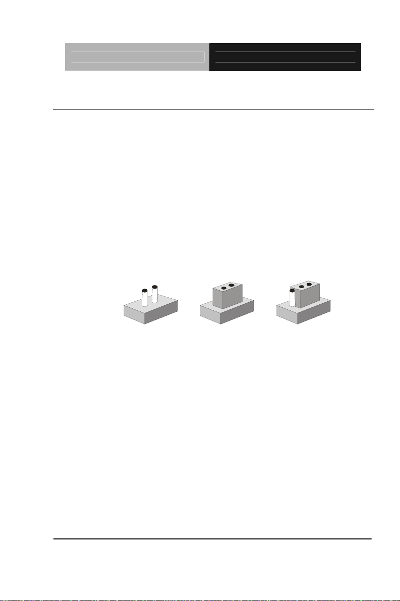
You configure your card to match the needs of your application by
setting jumpers. A jumper is the simplest kind of electric switch. It
consists of two metal pins and a small metal clip (often protected by a
plastic cover) that slides over the pins to connect them. To “close” a
jumper you connect the pins with the clip.
To “open” a jumper you remove the clip. Sometimes a jumper will have
three pins, labeled 1, 2 and 3. In this case you would connect either
pins 1 and 2 or 2 and 3.
3
2
1
Open Closed Closed 2-3
A pair of needle-nose pliers may be helpful when working with jumpers.
If you have any doubts about the best hardware configuration for your
application, contact your local distributor or sales representative before
you make any change.
Generally, you simply need a standard cable to make most
connections.
Chapter 2 Quick Installation Guide 2-10
Page 24
PC/104 Module PFM-CVS
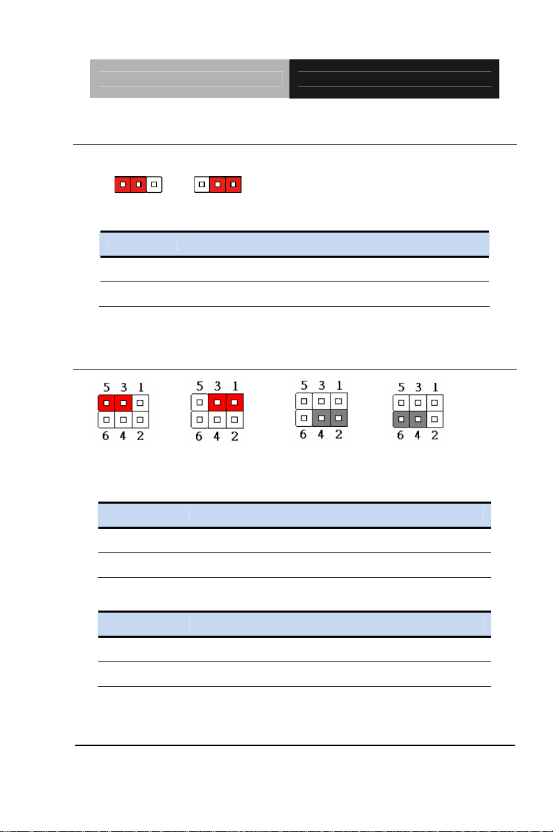
2.7 LVDS Voltage Selection (JP2)
123
+5V +3.3V
JP2 Function
1-2 +5V
2-3 +3.3V (Default)
123
2.8 AT/ATX Selection and LVDS Backlight Control Voltage
Selection (JP3)
+5V LVDS Backlight +12V LVDS Backlight ATX Mode AT Mode
LVDS Backlight
JP3 Function
1-3 +12V
3-5 +5V (Default)
ATX/AT Mode
JP3 Function
2-4 ATX
4-6 AT(Default)
Chapter 2 Quick Installation Guide 2-11
Page 25
PC/104 Module PFM-CVS
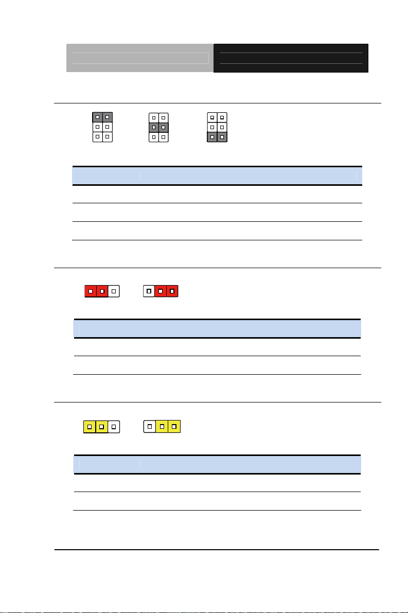
2.9 COM2 +5V/Ring/+12V Selection (JP6)
12
34
56
+12V Ring +5V
JP6 Function
1-2 +12V
3-4 Ring (Default)
5-6 +5V
12
34
56
12
34
56
2.10 PCI-104 VIO Voltage Selection (JP7)
123
+5V +3.3V
JP7 Function
1-2 +5V
2-3 +3.3V (Default)
123
2.11 Clear CMOS (JP8)
123
123
Normal Clear CMOS
JP8 Function
1-2 Normal (Default)
2-3 Clear CMOS
Chapter 2 Quick Installation Guide 2-12
Page 26

PC/104 Module PFM-CVS
2.12 PC/104 -5V/-12V Voltage Selection (JP11) Reserved
-12V -5V GND
JP11 Function
1 -12V
2 -5V
3 GND
2.13 Backlight Brightness Control Connector (CN2)
Pin Pin Name Signal T ype Signal Level
1 LVDS Voltage select OUT
2 LVDS Backlight control OUT
3 GND GND
4 GND GND
5 LVDS Backlight Enable OUT
Note: LVDS Voltage can be set to +5V or +12V by JP3.
Chapter 2 Quick Installation Guide 2-13
Page 27
PC/104 Module PFM-CVS
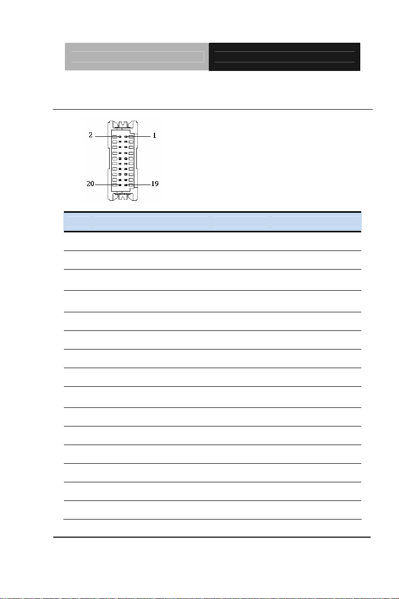
2.14 Internal LVDS Connector (CN3)
Pin Pin Name Signal T ype Signal Level
1 LVDS_BKLEN OUT
2 LVDS_BKLCTL OUT
3 LVDS Voltage PWR
4 LVDS Voltage PWR
5 LVDS_CLKN OUT
6 LVDS_TX2 OUT
+3.3V/
+5V
+3.3V/
+5V
7 LVDS_CLKP OUT
8 LVDS_TX#2 OUT
9 LVDS Voltage PWR
10 GND GND
11 LVDS_TX0 OUT
12 LVDS_TX3 OUT
13 LVDS_TX#0 OUT
14 LVDS_TX#3 OUT
15 GND GND
Chapter 2 Quick Installation Guide 2-14
+3.3V/
+5V
Page 28
PC/104 Module PFM-CVS
16 GND GND
17 LVDS_TX1 OUT
18 LVDS_DDCDAT I/O +3.3V
19 LVDS_TX#1 OUT
20 LVDS_DDCCLK I/O +3.3V
2.15 SATA Power Connector (CN5)
Pin Pin Name Signal T ype Signal Level
1 +5V PWR +5V
2 GND GND GND
2.16 PCI-104 Connector (CN6)
Standard PCI-104 Slot
2.17 Front Panel Connector (CN7)
Pin Pin Name Signal T ype Signal Level
1 POWER BUTTON IN
Chapter 2 Quick Installation Guide 2-15
Page 29
PC/104 Module PFM-CVS
2 POWRR BUTTON# IN
3 External Buzzer(+) OUT
4 External Buzzer(-) OUT
5 HDD LED OUT
6 HDD LED# OUT
7 POWER LED OUT
8 POWER LED# OUT
9 RESET IN
10 RESET# IN
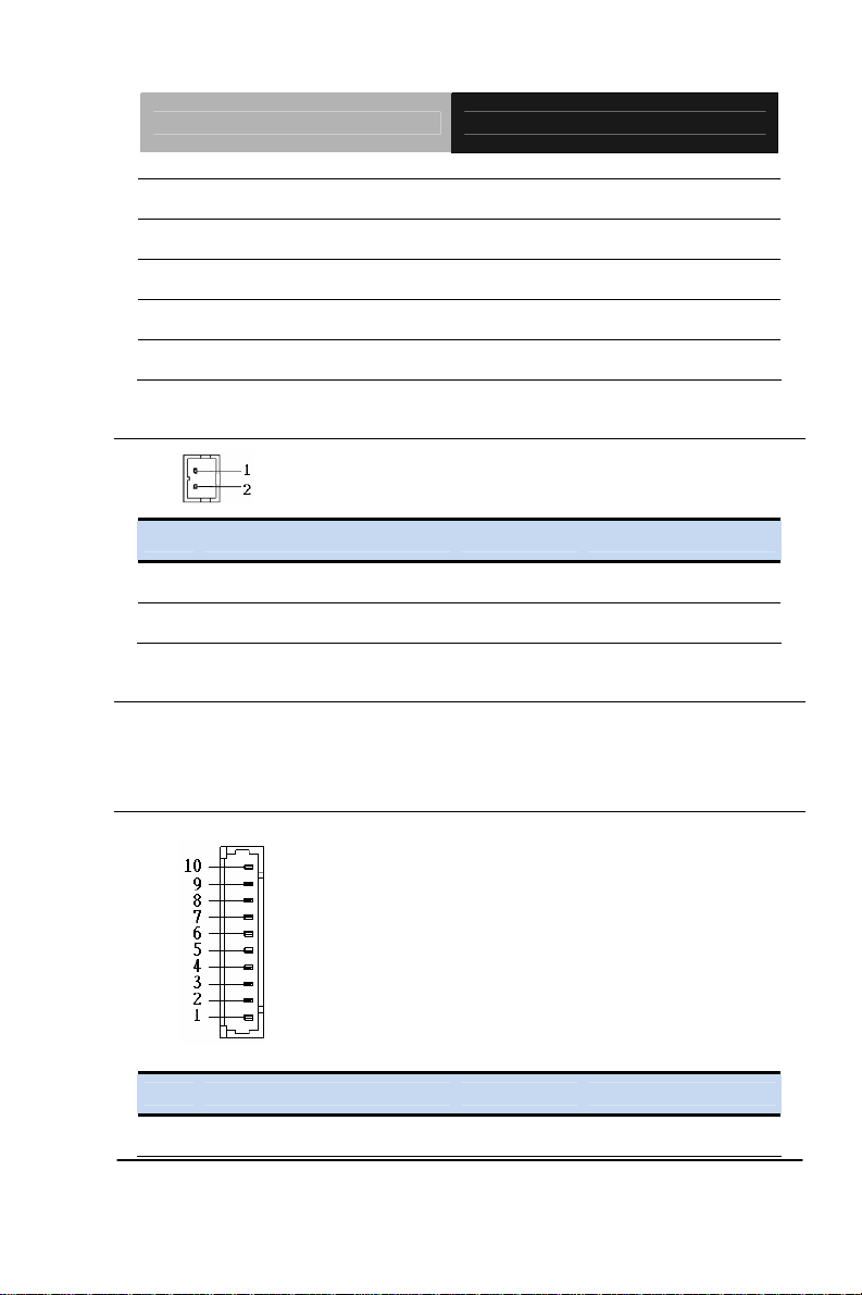
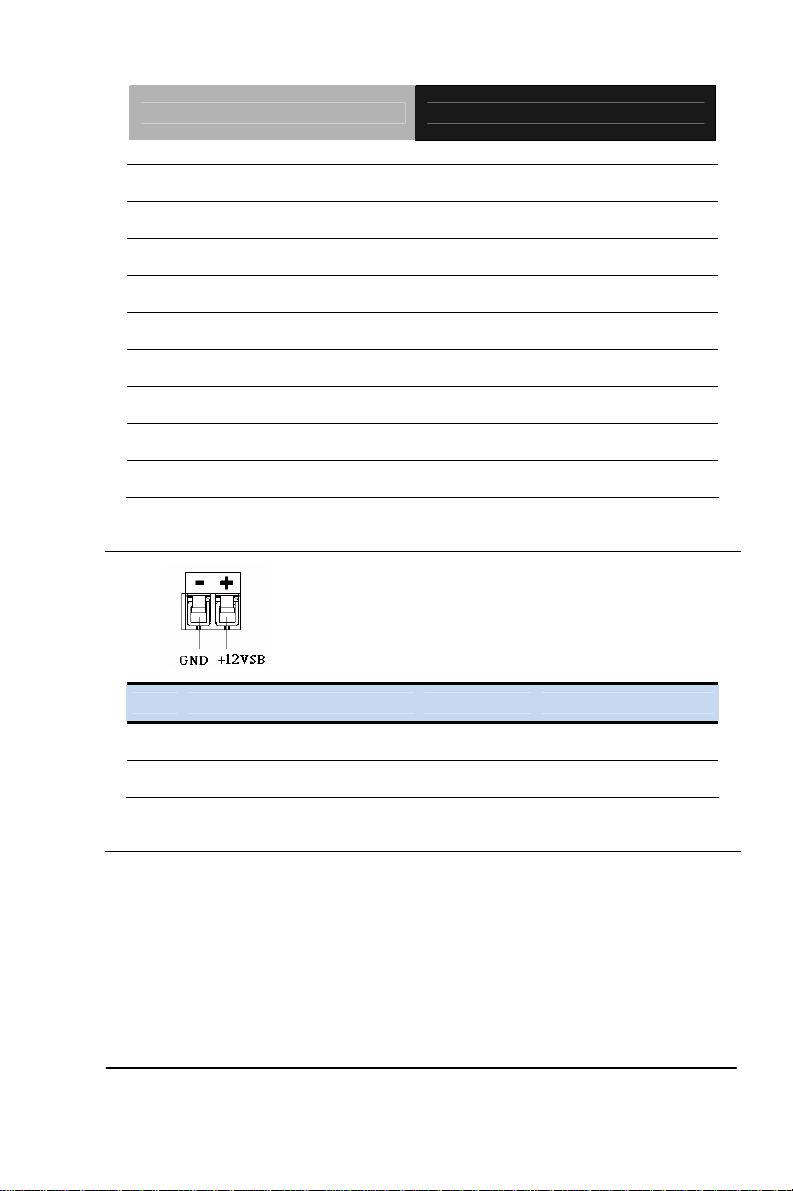
2.18 +12VSB Power Input Connector (CN9)
Pin Pin Name Signal T ype Signal Level
1 +12VSB PWR +12V
2 GND GND
2.19 PC/104/ ISA Connector (CN11)
Standard PC/104 / ISA Slot
Chapter 2 Quick Installation Guide 2-16
Page 30
PC/104 Module PFM-CVS
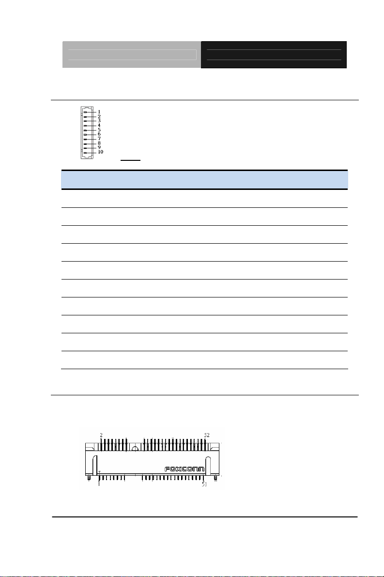
2.20 Digital I/O Connector (CN12)
Note: The DIO function has no ESD protection. It is only for
Pin Pin Name Signal type Signal Level
1 GPI0 IN
2 GPI1 IN
3 GPI2 IN
4 GPI3 IN
5 GPO0 OUT
6 GPO1 OUT
7 GPO2 OUT
8 GPO3 OUT
9 +3.3V PWR +3.3V
10 GND GND
non-isolation function.
2.21 Mini PCI Express/mSATA Connector (CN14) (Optional)
Standard Mini PCI Express Connector (52Pins)
Chapter 2 Quick Installation Guide 2-17
Page 31

PC/104 Module PFM-CVS
Pin Pin Name Signal T ype Signal Level
1 WAKE# I/O
2 +3V3_MC PWR +3.3V
3 Reserved
4 GND GND
5 Reserved
6 +1.5V PWR +1.5V
7 MC_CLKREQ# I/O
8 Reserved
9 GND GND
10 Reserved
11 PCIE_MC_CKLN OUT
12 Reserved
13 PCIE_MC_CKLP OUT
14 Reserved
15 GND GND
16 Reserved
17 Reserved
18 GND GND
19 Reserved
20 W_DISABLE#
21 GND GND
22 BUF_PLTRST# IN
23 PCIE_RXN1 DIFF
Chapter 2 Quick Installation Guide 2-18
Page 32

PC/104 Module PFM-CVS
24 +3V3_MC PWR +3.3V
25 PCIE_RXP1 DIFF
26 GND GND
27 GND GND
28 +1.5V PWR +1.5V
29 GND GND
30 SMBCLK_SBY I/O
31 PCIE_TXN1 DIFF
32 SMBDAT_SBY I/O
33 PCIE_TXP1 DIFF
34 GND GND
35 GND GND
36 USBP4- DIFF
37 GND GND
38 USBP4+ DIFF
39 +3V3_MC PWR +3.3V
40 GND GND
41 +3V3_MC PWR +3.3V
42 Reserved
43 GND GND
44 Reserved
45 Reserved
46 Reserved
47 Reserved
Chapter 2 Quick Installation Guide 2-19
Page 33

PC/104 Module PFM-CVS
48 +1.5V PWR +1.5V
49 Reserved
50 GND GND
51 Reserved
52 +3V3_MC PWR +3.3V
Standard mSATA Connector (52 Pins)
Pin Pin Name Signal T ype Signal Level
1 WAKE# I/O
2 +3V3_MC PWR +3.3V
3 Reserved
4 GND GND
5 Reserved
6 +1.5V PWR +1.5V
7 MC_CLKREQ# I/O
8 Reserved
9 GND GND
10 Reserved
11 PCIE_MC_CKLN OUT
12 Reserved
Chapter 2 Quick Installation Guide 2-20
Page 34

PC/104 Module PFM-CVS
13 PCIE_MC_CKLP OUT
14 Reserved
15 GND GND
16 Reserved
17 Reserved
18 GND GND
19 Reserved
20 W_DISABLE#
21 GND GND
22 BUF_PLTRST# IN
23 SATA_RXP1 DIFF
24 +3V3_MC PWR +3.3V
25 SATA_RXN1 DIFF
26 GND GND
27 GND GND
28 +1.5V PWR +1.5V
29 GND GND
30 SMBCLK_SBY I/O
31 SATA_TXN1 DIFF
32 SMBDAT_SBY I/O
33 SATA_TXP1 DIFF
34 GND GND
35 GND GND
36 USBP4- DIFF
Chapter 2 Quick Installation Guide 2-21
Page 35

PC/104 Module PFM-CVS
37 GND GND
38 USBP4+ DIFF
39 +3V3_MC PWR +3.3V
40 GND GND
41 +3V3_MC PWR +3.3V
42 Reserved
43 NC
44 Reserved
45 Reserved I/O
46 Reserved
47 Reserved I/O
48 +1.5V PWR +1.5V
49 Reserved I/O
50 GND GND
51 Reserved I/O
52 +3V3_MC PWR +3.3V
2.22 Battery Connector (BT1)
Pin Pin Name Signal Type Signal Level
1 RTCBAT PWR +3.3V
2 GND GND
Chapter 2 Quick Installation Guide 2-22
Page 36

PC/104 Module PFM-CVS
2.23 SATA Connector (SATA1)
Pin Pin Name Signal Type Signal Level
1 GND GND
2 SATA_TXP0 DIFF
3 SATA_TXN0 DIFF
4 GND GND
5 SATA_RXN0 DIFF
6 SATA_RXP0 DIFF
7 GND GND
2.24 CRT Connector (VGA1)
Pin Pin Name Signal Type Signal Level
1 VSYNC OUT
2 HSYNC OUT
Chapter 2 Quick Installation Guide 2-23
Page 37

PC/104 Module PFM-CVS
3 GND GND
4 SCL I/O +5V
5 SDA I/O +5V
6 GND GND
7 BLUE OUT
8 GND GND
9 GREEN OUT
10 GND GND
11 RED OUT
12 GND GND
13 VCC PWR +5V
2.25 COM1 RS-232 Connector (COM1)
Pin Pin Name Signal Type Signal Level
1 DCD1 IN
2 DSR1 IN
3 RXD1 IN
4 RTS1 OUT ±9V
5 TXD1 OUT ±9V
6 CTS1 IN
Chapter 2 Quick Installation Guide 2-24
Page 38

PC/104 Module PFM-CVS
7 DTR1 OUT ±9V
8 RI1 IN
9 GND GND
2.26 COM2 RS-232/422/485 Connector (COM2)
RS-232
Pin Pin Name Signal Type Signal Level
1 DCD2 IN
2 DSR2 IN
3 RXD2 IN
4 RTS2 OUT ±9V
5 TXD2 OUT ±9V
6 CTS2 IN
7 DTR2 OUT ±9V
8 RI2 IN
9 GND GND
RS-422
Pin Pin Name Signal Type Signal Level
1 TX- OUT ±5V
Chapter 2 Quick Installation Guide 2-25
Page 39

PC/104 Module PFM-CVS
2 N.C
3 RX+ IN
4 N.C
5 TX+ OUT ±5V
6 N.C
7 RX- IN
8 +5V/+12V PWR +5V/+12V
9 GND GND
RS-485
Pin Pin Name Signal Type Signal Level
1 B (Data-) I/O ±5V
2 N.C
3 N.C
4 N.C
5 A (Data+) I/O ±5V
6 N.C
7 N.C
8 +5V/+12V PWR +5V/+12V
9 GND GND
2.27 COM3 RS-232 Connector (COM3)
Chapter 2 Quick Installation Guide 2-26
Page 40

PC/104 Module PFM-CVS
Pin Pin Name Signal Type Signal Level
1 DCD3 IN
2 DSR3 IN
3 RXD3 IN
4 RTS3 OUT ±9V
5 TXD3 OUT ±9V
6 CTS3 IN
7 DTR3 OUT ±9V
8 RI3 IN
9 GND GND
2.28 COM4 RS-232 Connector (COM4)
Pin Pin Name Signal Type Signal Level
1 DCD4 IN
2 DSR4 IN
3 RXD4 IN
4 RTS4 OUT ±9V
5 TXD4 OUT ±9V
6 CTS4 IN
7 DTR4 OUT ±9V
Chapter 2 Quick Installation Guide 2-27
Page 41

PC/104 Module PFM-CVS
8 RI4 IN
9 GND GND
2.29 USB2.0 Connector (USB1)
Pin Pin Name Signal Type Signal Level
1 USB_VCC0 PWR +5V
2 USBP0- OUT
3 USBP0+ OUT
4 GND GND
5 GND GND
2.30 USB2.0 Connector (USB2)
Pin Pin Name Signal Type Signal Level
1 USB_VCC0 PWR +5V
2 USBP1- OUT
3 USBP1+ OUT
4 GND GND
5 GND GND
Chapter 2 Quick Installation Guide 2-28
Page 42

PC/104 Module PFM-CVS
2.31 USB2.0 Connector (USB3)
Pin Pin Name Signal Type Signal Level
1 USB_VCC1 PWR +5V
2 USBP2- OUT
3 USBP2+ OUT
4 GND GND
5 GND GND
2.32 USB2.0 Connector (USB4)
Pin Pin Name Signal Type Signal Level
1 USB_VCC1 PWR +5V
2 USBP3- OUT
3 USBP3+ OUT
4 GND GND
5 GND GND
Chapter 2 Quick Installation Guide 2-29
Page 43

PC/104 Module PFM-CVS
2.33 FAN Connector (FAN1) Reserved
Pin Pin Name Signal Type Signal Level
1 GND GND
2 FAN_CTL OUT
3 FAN_TAC IN
2.34 LAN Connector (LAN1)
Pin Pin Name Signal Type Signal Level
1 LAN1_TX1+ DIFF.
2 LAN1_TX1- DIFF.
3 LAN1_RX1+ DIFF.
4 LAN1_RX1- DIFF.
5 GND GND
6 GND GND
7 LAN1_TX2+ DIFF.
8 LAN1_TX2- DIFF.
9 LAN1_RX2+ DIFF
Chapter 2 Quick Installation Guide 2-30
Page 44

PC/104 Module PFM-CVS
10 LAN1_RX2- DIFF
2.35 DDR3 SODIMM Connector (DIMM1)
Standard DDR3 SODIMM Specification
Chapter 2 Quick Installation Guide 2-31
Page 45

PC/104 Module PFM-CVS
Below Table for China RoHS Requirements
产品中有毒有害物质或元素名称及含量
AAEON Main Board/ Daughter Board/ Backplane
有毒有害物质或元素
部件名称
印刷电路板
及其电子组件
外部信号
连接器及线材
O:表示该有毒有害物质在该部件所有均质材料中的含量均在
SJ/T 11363-2006 标准规定的限量要求以下。
X:表示该有毒有害物质至少在该部件的某一均质材料中的含量超出
SJ/T 11363-2006 标准规定的限量要求。
备注:此产品所标示之环保使用期限,系指在一般正常使用状况下。
铅
(Pb)汞 (Hg)镉 (Cd)
× ○ ○ ○ ○ ○
× ○ ○ ○ ○ ○
六价铬
(Cr(VI))
多溴联苯
(PBB)
多溴二苯醚
(PBDE)
Chapter 2 Quick Installation Guide 2-32
Page 46

PC/104 Module PFM-CVS
Chapter
3
AMI
BIOS Setup
Chapter 3 AMI BIOS Setup 3-1
Page 47

PC/104 Module PFM-CVS
3.1 System Test and Initialization
These routines test and initialize board hardware. If the routines
encounter an error during the tests, you will either hear a few short
beeps or see an error message on the screen. There are two kinds
of errors: fatal and non-fatal. The system can usually continue the
boot up sequence with non-fatal errors.
System configuration verification
These routines check the current system configuration stored in the
CMOS memory and BIOS NVRAM. If system configuration is not
found or system configuration data error is detected, system will
load optimized default and re-boot with this default system
configuration automatically.
There are four situations in which you will need to setup system
configuration:
1. You are starting your system for the first time
2. You have changed the hardware attached to your system
3. The system configuration is reset by Clear-CMOS jumper
4. The CMOS memory has lost power and the configuration
information has been erased.
The PFM-CVS CMOS memory has an integral lithium battery
backup for data retention. However, you will need to replace the
complete unit when it finally runs down.
Chapter 3 AMI BIOS Setup 3-2
Page 48

PC/104 Module PFM-CVS
3.2 AMI BIOS Setup
AMI BIOS ROM has a built-in Setup program that allows users to
modify the basic system configuration. This type of information is
stored in battery-backed CMOS RAM and BIOS NVRAM so that it
retains the Setup information when the power is turned off.
Entering Setup
Power on the computer and press <Del>or <F2> immediately. This
will allow you to enter Setup.
Main
Set the date, use tab to switch between date elements.
Advanced
Enable disable boot option for legacy network devices.
Chipset
Host bridge parameters.
Boot
Enables/disable quiet boot option.
Security
Set setup administrator password.
Save&Exit
Exit system setup after saving the changes.
Chapter 3 AMI BIOS Setup 3-3
Page 49

PC/104 Module PFM-CVS
Setup Men
u
Setup submenu: Main
Chapter 3 AMI BIOS Setup 3-4
Page 50

PC/104 Module PFM-CVS
Setup submenu: Advanced
Chapter 3 AMI BIOS Setup 3-5
Page 51

PC/104 Module PFM-CVS
ACPI Settings
Options summary :
S3 (Suspend to RAM) Optimal Default, Failsafe DefaultSuspend mode
Select the ACPI state used for System Suspend
Chapter 3 AMI BIOS Setup 3-6
Page 52

PC/104 Module PFM-CVS
CPU Configuration
Options summary :
Disabled Hyper-Threading
Enabled Optimal Default, Failsafe Default
En/Disable CPU Hyper-Threading function
Chapter 3 AMI BIOS Setup 3-7
Page 53

PC/104 Module PFM-CVS
IDE Configuration (IDE)
Chapter 3 AMI BIOS Setup 3-8
Page 54

PC/104 Module PFM-CVS
IDE Configuration (AHCI)
Options summary :
Disabled SATA Controllers
En/Disable SATA Controller.
IDE: Configure SATA controllers as legacy IDEAHCI: Configure SATA controllers to
operate in AHCI mode
En/Disable Hot Plug feature.
Enabled Default
IDE Default SATA Mode
AHCI
Disabled Hot Plug
Enabled Optimal Default, Failsafe Default
Chapter 3 AMI BIOS Setup 3-9
Page 55

PC/104 Module PFM-CVS
USB Configuration
Options summary :
Legacy USB Support
Enables BIOS Support for Legacy USB Support. When enabled, USB can be
functional in legacy environment like DOS.
AUTO option disables legacy support if no USB devices are connected
Device Name (Emulation
Type)
If Auto. USB devices less than 530MB will be emulated as Floppy and remaining as
Floppy and remaining as hard drive. Forced FDD option can be used to force a HDD
formatted drive to boot as FDD(Ex. ZIP drive)
Enabled Optimal Default, Failsafe Default
Disabled
Auto
Auto Optimal Default, Failsafe Default
Floppy
Forced FDD
Hard Disk
CDROM
Chapter 3 AMI BIOS Setup 3-10
Page 56

PC/104 Module PFM-CVS
F81866 Super IO Configuration
Chapter 3 AMI BIOS Setup 3-11
Page 57

PC/104 Module PFM-CVS
Serial Port
Con
figuration
Chapter 3 AMI BIOS Setup 3-12
Page 58

PC/104 Module PFM-CVS
Chapter 3 AMI BIOS Setup 3-13
Page 59

PC/104 Module PFM-CVS
Chapter 3 AMI BIOS Setup 3-14
Page 60

PC/104 Module PFM-CVS
Options summary :
Disabled Serial Port
Allows BIOS to En/Disable correspond serial port.
Change Settings
(Serial Port 1)
Allows BIOS to Select Serial Port resource.
Change Settings
(Serial Port 2)
Allows BIOS to Select Serial Port resource.
Change Settings
(Serial Port 3)
Allows BIOS to Select Serial Port resource.
Change Settings
(Serial Port 4)
Allows BIOS to Select Serial Port resource.
Power Failure
Select the action system to take when restoring from power loss.
En/Disable ERP power saving function.
Enabled Default
Auto Default
IO=3F8h; IRQ=4;
IO=3F8h; IRQ=3,4;
IO=2F8h; IRQ=3,4;
Auto Default
IO=2F8h; IRQ=3;
IO=3F8h; IRQ=3,4;
IO=2F8h; IRQ=3,4;
Auto Default
IO=3E8h; IRQ=11;
IO=3E8h; IRQ=10,11;
IO=2E8h; IRQ=10,11;
Auto Default
IO=2E8h; IRQ=10;
IO=3E8h; IRQ=10,11;
IO=2E8h; IRQ=10,11;
Keep last state Default
Always on
Always off
Disabled Default ERP Function
Enabled
Chapter 3 AMI BIOS Setup 3-15
Page 61

PC/104 Module PFM-CVS
F81866 H/W Monitor
Chapter 3 AMI BIOS Setup 3-16
Page 62

PC/104 Module PFM-CVS
Digital IO
Options summary :
Input Default DIO_P#1~4
Allows BIOS to select input/output function to corresponding DIO ping.
Allows BIOS to select input/output function to corresponding DIO ping.
Allows BIOS to select high/low voltage level to output to corresponding DIO ping.
Output
Input DIO_P#5~8
Output Default
Low DIO_P#1~8 Direction
Hi Default
Chapter 3 AMI BIOS Setup 3-17
Page 63

PC/104 Module PFM-CVS
Setup submenu: Chipset
Chapter 3 AMI BIOS Setup 3-18
Page 64

PC/104 Module PFM-CVS
Host Bridge
Chapter 3 AMI BIOS Setup 3-19
Page 65

PC/104 Module PFM-CVS
Graphics Configuration
Chapter 3 AMI BIOS Setup 3-20
Page 66

PC/104 Module PFM-CVS
Options summary :
Size
Select the amount of system memory used by the Internal graphics device.
IGFX - Boot Type
Select boot display device.
En/Disable LVDS interface
LCD Panel Type
Select panel native resolution.
Select backlight control type
LCDS Backlight Level 0~100% Default 80%
Select backlight control output value
128MB Fixed Graphics Memory
256MB Default
VBIOS Default Default
CRT
LFP
No LVDS Active LFP
LVDS Default
VBIOS Default Default
640x480 18bit
800x600 18bit
1024x768 18bit
1366x768 18bit
1280x768 18bit
PWM Inverted Backlight Control
PWM Normal Default
Chapter 3 AMI BIOS Setup 3-21
Page 67

PC/104 Module PFM-CVS
South Bridge
Options summary :
ATX Type Default Power Mode
Select Power Mode:
ATX Type: Normal ACPI support
AT Type: Suspend/Sleep disabled, and Always On when restoring from power
failure.
Enabling/Disabling PCI Express root ports
PCI Express Root Port x
Enabling/Disabling PCI Express root ports
AT Type
Disabled PCI Express Root Port 0
Enabled Default
Disabled
Enabled
Auto Default
Chapter 3 AMI BIOS Setup 3-22
Page 68

PC/104 Module PFM-CVS
Setup submenu: Boot
Options summary :
Disabled Quiet Boot
Enabled Default
En/Disable showing boot logo.
Disabled Default Launch PXE OpROM
Enabled
En/Disable PXE boot from LAN
Chapter 3 AMI BIOS Setup 3-23
Page 69

PC/104 Module PFM-CVS
BBS Priorities
Chapter 3 AMI BIOS Setup 3-24
Page 70

PC/104 Module PFM-CVS
Security
Change User/Supervisor Password
You can install a Supervisor password, and if you install a supervisor password, you
can then install a user password. A user password does not provide access to
many of the features in the Setup utility.
If you highlight these items and press Enter, a dialog box appears which lets you
enter a password. You can enter no more than six letters or numbers. Press
Enter after you have typed in the password. A second dialog box asks you to
retype the password for confirmation. Press Enter after you have retyped it
correctly. The password is required at boot time, or when the user enters the Setup
utility.
Chapter 3 AMI BIOS Setup 3-25
Page 71

PC/104 Module PFM-CVS
Removing the Password
Highlight this item and type in the current password. At the next dialog box press
Enter to disable password protection.
Chapter 3 AMI BIOS Setup 3-26
Page 72

PC/104 Module PFM-CVS
Setup submenu: Exit
Chapter 3 AMI BIOS Setup 3-27
Page 73

PC/104 Module PFM-CVS
Chapter
4
Driver
Inst
allation
Chapter 4 Driver Installation 4 - 1
Page 74

PC/104 Module PFM-CVS
The PFM-CVS comes with a CD-ROM that contains all drivers and
utilities that meet your needs.
Follow the sequence below to install the drivers:
Step 1 – Install Chipset Driver
Step 2 – Install VGA Driver
Step 3 – Install LAN Driver
Step 4 – Install Serial Port Driver (Optional)
Step 5 – Install Rapid Storage Technology
Step 6 – Install AHCI for XP Installation
Please read instructions below for further detailed installations.
Chapter 4 Driver Installation 4 - 2
Page 75

PC/104 Module PFM-CVS
4.1 Installation:
Insert the PFM-CVS CD-ROM into the CD-ROM Drive. And install
the drivers from Step 1 to Step 6 in order.
Step 1 – Install Chipset Driver
1. Click on the Step 1 – Chipset folder and double click on
the Setup.exe file
2. Follow the instructions that the window shows
3. The system will help you install the driver automatically
Step 2 – Install VGA Driver
1. Click on the Step 2 – VGA folder and select the OS your
system is
2. Double click on the .exe file located in each OS folder
3. Follow the instructions that the window shows
4. The system will help you install the driver automatically
Step 3 – Install LAN Driver
1. Click on the STEP3 – LAN folder and select the OS your
system is
2. Double click on the setup.exe file located in each OS
folder
3. Follow the instructions that the window shows
4. The system will help you install the driver automatically
Chapter 4 Driver Installation 4 - 3
Page 76

PC/104 Module PFM-CVS
Step 4 – Inst all Serial Port Driver (Optional)
For Wind
ows® XP 32-bit
1. Click on the STEP4 - Serial Port Driver (Optional) folder
and select the OS folder of WINXP_32
2. Double click on the patch.bat file
3. The system will help you install the driver automatically
4. Check the driver installation in the device manager
Chapter 4 Driver Installation 4 - 4
Page 77

PC/104 Module PFM-CVS
For Windows
®
7 32-bit/ 64-bit
1. Modify the UAC (User Account Control) setting to Never
notify
Chapter 4 Driver Installation 4 - 5
Page 78

PC/104 Module PFM-CVS
2. Restart the operating system.
Chapter 4 Driver Installation 4 - 6
Page 79

PC/104 Module PFM-CVS
3. Click on the STEP4 - Serial Port Driver (Optional) folder
and select the OS folder.
4. Right click on the patch.bat file and select Run as
administrator
5. The system will help you install the driver automatically.
6. Check the driver installation in the device manager.
Chapter 4 Driver Installation 4 - 7
Page 80

PC/104 Module PFM-CVS
Step 5 – Install Rapid Storage Technology
1. Click on the Step5 - Rapid Storage Technology folder
and select the OS your system is
2. Double click on the setup.exe file located in each OS
folder
3. Follow the instructions that the window shows
4. The system will help you install the driver automatically
Step 6 – Install AHCI for XP Installation
Note: BIOS Setting Requirement : “BIOS SettingAdvanced Launch
Storage OpROM : Enable to enable HDD”
Chapter 4 Driver Installation 4 - 8
Page 81

PC/104 Module PFM-CVS
Step 1: Copy the files below from “Driver CD” -> “Step6 - AHCI for XP
installation” to Disk.
Step 2: Setup OS
Step 3: Press “F6”
Chapter 4 Driver Installation 4 - 9
Page 82

PC/104 Module PFM-CVS
Step 4: Choose “S”
Step 5: Choose “Intel(R) NM10 Express Chipset”
Chapter 4 Driver Installation 4 - 10
Page 83

PC/104 Module PFM-CVS
Step 6: It will show the model number you select and then press “ENTER”
Step 7: Setup is starting Windows
Chapter 4 Driver Installation 4 - 11
Page 84

PC/104 Module PFM-CVS
A
Appendix
Programming the
atchdog Timer
W
Appendix A Programming the Watchdog Timer A-1
Page 85

PC/104 Module PFM-CVS
A.1 Programming
PFM-CVS utilizes FINTEK 81866 chipset as its wat ch dog timer
controller. Below are the procedures to complete its configuration
and the AAEON initial watchdog timer program is also
attached based on which you can develop customized
program to fit your application.
Configuring Sequence Description
After the hardware reset or power-on reset, the FINTEK 81866
enters the normal mode with all logical devices disabled
except KBC. The initial state (enable bit ) of this logical device
(KBC) is determined by the state of pin 121 (DTR1#) at the falling
edge of the system reset during power-on reset.
Appendix A Programming the Watchdog Timer A-2
Page 86

PC/104 Module PFM-CVS
There are three steps to complete the configuration setup: (1) Enter
the MB PnP Mode; (2) Modify the data of configuration re gisters; (3)
Exit the MB PnP Mode. Undesired result may occur if the MB PnP
Mode is not exited normally.
(1) Enter the MB PnP Mode
To enter the MB PnP Mode, four special I/O write operations are to
be performed during Wait for Key st ate. To ensure the initial state of
the key-check logic, it is necessary to p erform four write opera-tio ns
to the Special Address port (2EH). Two different enter keys are
provided to select configuration ports (2Eh/2Fh) of the next step.
(2) Modify the Data of the Regist ers
All configuration registers can be accessed after entering the MB
PnP Mode. Before accessing a selected register, the content of
Index 07h must be changed to the LDN to which the register
belongs, except some Global registers.
(3) Exit the MB PnP Mode
Write exit key 0xAA to the index port.
Appendix A Programming the Watchdog Timer A-3
Page 87

PC/104 Module PFM-CVS
Watch Dog Timer 1, 2, 3 Control Register (Index=F5h,F6h,FAh
Default=00h)
Appendix A Programming the Watchdog Timer A-4
Page 88

PC/104 Module PFM-CVS
A.2 F81866 Watchdog Timer Initial Program
Main(){
aaeonSuperIOOpen();
aaeonWdtSetCountMode(BOOLbMinute);//Setwdtcountmode
aaeonWdtSetTimeoutCount(BYTEtTimeout);//Setwdttimer
aaeonWdtSetEnable(BOOLbEnable);//Enablewdt
aaeonSuperIOClose();
}
VoidaaeonSuperIOOpen(){ //ConfigF81866Entrykey
aaeonioWritePortByte(F81866_INDEX,0x87);
aaeonioWritePortByte(F81866_INDEX,0x87);
}
VoidaaeonWdtSetCountMode(BOOLbMinute){
BYTEWDT_CONTROL=f81866ReadByte(F81866_WDT_CONTROL_REG);
if(bMinute)
f81866WriteByte(F81866_WDT_CONTROL_REG,WDT_CONTROL|0x08);
else
f81866WriteByte(F81866_WDT_CONTROL_REG,WDT_CONTROL&0xF7);
}
Appendix A Programming the Watchdog Timer A-5
Page 89

PC/104 Module PFM-CVS
VoidaaeonWdtSetTimeoutCount(BYTEtTimeout){
f81866SetLdn(0x07);
f81866WriteByte(F81866_WDT_TIME_REG,tTimeout);
}
VoidaaeonWdtSetEnable(BOOLbEnable){
f81866SetLdn(0x07);
if(bEnable){
f81866WriteByte(0x30,0x01);
WDT_BASE_ADDR=
(f81866ReadByte(F81866_WDT_BASEADDR_REG_MSB)<<8)
|f81866ReadByte(F81866_WDT_BASEADDR_REG_LSB);
WDT_STATUS=f81866ReadByte(F81866_WDT_CONTROL_REG);
f81866WriteByte(F81866_WDT_CONTROL_REG,WDT_STATUS|0x20);
WDT_STATUS=f81866ReadByte(F81866_WDT_PME_REG);
f81866WriteByte(F81866_WDT_PME_REG,WDT_STATUS|0x01);
}else{
f81866WriteByte(0x30,0x00);
WDT_BASE_ADDR=0;
WDT_STATUS=f81866ReadByte(F81866_WDT_CONTROL_REG);
f81866WriteByte(F81866_WDT_CONTROL_REG,WDT_STATUS&0xDF);
WDT_STATUS=f81866ReadByte(F81866_WDT_PME_REG);
f81866WriteByte(F81866_WDT_PME_REG,WDT_STATUS&0xFE);
}
}
Appendix A Programming the Watchdog Timer A-6
Page 90

PC/104 Module PFM-CVS
VoidaaeonSuperIOClose(){
aaeonioWritePortByte(F81866_INDEX,0xaa);
}
Appendix A Programming the Watchdog Timer A-7
Page 91

PC/104 Module PFM-CVS
Appendix
B
I/O Information
Appendix B I/O Information B-1
Page 92

PC/104 Module PFM-CVS
B.1 I/O Address Map
Appendix B I/O Information B-2
Page 93

PC/104 Module PFM-CVS
Appendix B I/O Information B-3
Page 94

PC/104 Module PFM-CVS
st
MB Memory Address Map
B.2 1
Appendix B I/O Information B-4
Page 95

PC/104 Module PFM-CVS
B.3 IRQ Mapping Chart
Appendix B I/O Information B-5
Page 96

PC/104 Module PFM-CVS
Appendix B I/O Information B-6
Page 97

PC/104 Module PFM-CVS
B.4 DMA Channel Assignments
Appendix B I/O Information B-7
Page 98

PC/104 Module PFM-CVS
Appendix
C
Mating Connector
Appendix C Mating Connector C - 1
Page 99

PC/104 Module PFM-CVS
C.1 List of Mating Connectors and Cables
The table notes mating connectors and available cables.
Connector
Label
Function
Mating Connector
Vendor Model number
Available
Cable
Cable P/N
CN2 Backlight
Brightness
Control
(Dummy)
CN3 Internal
LVDS
CN5 SATA Power CATCH H732-02 CATCH 1702150155
CN7 Front Panel
CN7 Front Panel
CN7 Front Panel
CN9 +12VSB
CN12 Digital I/O
CN12 Digital I/O
LAN1
VGA1 CRT
COM1
Appendix C Mating Connector C - 2
(Dummy)
(External
10Pins
Header)
(External
2Pins
Buzzer)
Power Input
(Dummy)
(External10
Pins
Connector)
LAN
Connector
Connector
COM1
RS232
Connector
CATCH H738-05 CATCH 1705050153
HIROSE DF13-20S-1.25C Great
Ideal
CATCH H752-10 CATCH 1701010150
CATCH H752-10 CATCH 1701100155
CATCH H752-10 CATCH 1703020156
N/A N/A CATCH 1702002010
CATCH H752-10 CATCH 1701010150
CATCH H752-10 CATCH 1700100408
CATCH H820-2-10 CATCH 1700100201
CATCH H752-13 CATCH 1709150151
CATCH H752-09 CATCH 1701090150
1704200200
Page 100

COM2
COM3
COM4
USB1
USB2
USB3
USB4
PC/104 Module PFM-CVS
COM2
RS232/422/
485
Connector
COM3
RS232
Connector
COM4
RS232
Connector
USB2.0
Connector
USB2.0
Connector
USB2.0
Connector
USB2.0
Connector
CATCH H752-09 CATCH 1701090150
CATCH H752-09 CATCH 1701090150
CATCH H752-09 CATCH 1701090150
CATCH H752-05 CATCH 1700050207
CATCH H752-05 CATCH 1700050207
CATCH H752-05 CATCH 1700050207
CATCH H752-05 CATCH 1700050207
Appendix C Mating Connector C - 3
 Loading...