

Page 1

PC 104 CPU Module PFM-540I
AMD® Geode
AMD LX 800 +CS 5536
RTL8139DL for 10/100Mbps
18/24-bit TFT LCD Panel
2 COM, 4 USB, 1 IrDA
PFM-540I
LX 800 Processor
PFM-540I Manual Rev.A 1st Ed.
NOV. 2006
Page 2

PC 104 CPU Module PFM-540I
Copyright Notice
This document is copyrighted, 2006. All rights are reserved. The
original manufacturer reserves the right to make improvements
to the products described in this manual at any time without
notice.
No part of this manual may be reproduced, copied, translated,
or transmitted in any form or by any means without the prior
written permission of the original manufacturer. Information
provided in this manual is intended to be accurate and reliable.
However, the original manufacturer assumes no responsibility
for its use, or for any infringements upon the rights of third
parties that may result from its use.
The material in this document is for product information only
and is subject to change without notice. While reasonable
efforts have been made in the preparation of this document to
assure its accuracy, AAEON assumes no liabilities resulting
from errors or omissions in this document, or from the use of the
information contained herein.
AAEON reserves the right to make changes in the product
design without notice to its users.
i
Page 3

PC 104 CPU Module PFM-540I
Acknowledgments
All other products’ name or trademarks are properties of their
respective owners.
Award is a trademark of Award Software International, Inc.
CompactFlash™ is a trademark of the Compact Flash
Association.
Intel
Microsoft Windows
AMD Geode ® is a registered trademark of Advanced Micro
ITE is a trademark of Integrated Technology Express, Inc.
IBM, PC/AT, PS/2, and VGA are trademarks of International
SoundBlaster is a trademark of Creative Labs, Inc.
®
, Pentium® M, and Celeron® M are trademarks of Intel®
Corporation.
®
is a registered trademark of Microsoft Corp.
Devices, Inc.
Business Machines Corporation.
All other product names or trademarks are properties of their
respective owners.
ii
Page 4

PC 104 CPU Module PFM-540I
Packing List
Before you begin installing your card, please make sure that the
following materials have been shipped:
9681540I00
Cable Kit for PFM-540I
1701160201 VGA cable x 1
1701260201 Printer Port Cable x 1
1709100201 USB Cable x 1
1700100200 LAN Cable x 1
1700060152 Keyboard & Mouse Cable x 1
1701440350 44-pin IDE Cable x 1
1701100207 RS-232 Cable x 2
1701340703 Floppy Disk Cable x 1
9657666600
Jumper Cap
Quick Installation Guide
Utility CD
PFM-540I
If any of these items should be missing or damaged, please
contact your distributor or sales representative immediately.
iii
Page 5

PC 104 CPU Module PFM-540I
Contents
Chapter 1 General Information
1.1 Introduction................................................................ 1-2
1.2 Features....................................................................1-3
1.3 Specifications............................................................ 1-4
Chapter 2 Quick Installation Guide
2.1 Safety Precautions.................................................... 2-2
2.2 Location of Connectors and Jumpers .......................2-3
2.3 Mechanical Drawing..................................................2-5
2.4 List of Jumpers..........................................................2-7
2.5 List of Connectors .....................................................2-8
2.6 Setting Jumpers ........................................................2-9
2.7 CFD Master/ Slave Selection (JP1) ..........................2-10
2.8 RS-232 Ring/5V Selection (JP2)...............................2-10
2.9 LCD Clock Selection and Clear CMOS (JP3)........... 2-10
2.10 Front Panel Connector (CN1) .................................2-11
2.11 PS2 Keyboard/Mouse Connector (CN2).................2-11
2.12 Option Power Connector (CN3).............................. 2-12
2.13 USB 3-4 Connector (CN4) ......................................2-12
2.14 VGA Display Connector (CN5)................................ 2-12
2.15 USB 1-2 Connector (CN6) ......................................2-13
2.16 PC 104 Connector (CN7)........................................2-13
2.17 LPT Port Connector (CN8)......................................2-13
iv
Page 6

PC 104 CPU Module PFM-540I
2.18 IDE Connector (CN9).............................................. 2-14
2.19 COM1 Connector (CN10)........................................ 2-15
2.20 Floppy Connector (CN11).......................................2-16
2.21 Power Connector (CN12)........................................2-17
2.22 COM 2 Connector (CN13)....................................... 2-17
2.23 Ethernet Connector (CN14) ....................................2-17
2.24 LCD Connector (CN15)...........................................2-18
2.25 Battery Connector (BAT1).......................................2-20
2.26 DDR 1 SODIMM Slot (SODIMM1).......................... 2-20
Chapter 3 Award BIOS Setup
3.1 System Test and Initialization. ..................................3-2
3.2 Award BIOS Setup.................................................... 3-3
Chapter 4 Driver Installation
4.1 Software Drivers........................................................ 4-2
4.2 Necessary to know....................................................4-3
4.3 Installing VGA Driver.................................................4-4
4.4 Installing AES Driver .................................................4-5
4.5 Installing PCI to ISA Bridge Driver............................ 4-6
4.6 Installing Ethernet Driver...........................................4-7
4.7 Ethernet Software Configuration...............................4-7
Appendix A Programming The Watchdog Timer
A.1 Programming .........................................................A-2
A.2 IT8712F-A Watchdog Timer Initial Program..........A-6
v
Page 7

PC 104 CPU Module PFM-540I
Appendix B I/O Information
B.1 I/O Address Map....................................................B-2
B.2 Memory Address Map............................................B-3
B.3 IRQ Mapping Chart................................................B-4
B.4 DMA Channel Assignments...................................B-4
Appendix C Mating Connector
C.1 List of Mating Connectors and Cables.................. C-2
vi
Page 8

PC 104 CPU Module PFM-540I
Information
Chapter
1
General
Chapter 1 General Information 1- 1
Page 9

PC 104 CPU Module PFM-540I
1.1 Introduction
AAEON Technology, a leading company in embedded boards
manufacturing with a full range of PC/104 CPU Modules,
launches an economic version PC/104 CPU Module-PFM-540I.
Its compact size and rich functionality ensures the most cost
effective and compatible module to coincide with your existing
system planning devices.
PFM-540I adopts an AMD Geode LX800 processor that is more
cost effective compared to other PC/104 CPU modules on the
market. This model supports DDR 333 SODIMM Memory up to
1GB (DDR 400 optional). Although PFM-540I is a small board,
it offers the full functions customers demand. The chipset of
PFM-540I deploys AMD LX800 and CS5536 that makes this
board achieve high performance. It features one
10/100Base-TX Ethernet port, four USB 2.0 ports, two serial
ports, one parallel port, IR interface, watchdog timer and includes
PC/104 expansion.
PFM-540I is a RoHS compliant product that is fanless and fully
supports ISA and CFD. For Operating Systems, it supports
regular embedded OS, such as WinCE, and WinXP Embedded,
Windows XP Professional for easy compatibility with customers’
existing OS systems.
Chapter 1 General Information 1- 2
Page 10

PC 104 CPU Module PFM-540I
1.2 Features
AMD Geode LX800 (500MHz) Processor
Supports Onboard DDR SDRAM, Max. 1GB for DDR333
and 512MB for DDR400
Supports 18/24-bit TFT LCD panel
Supports CFD Type I, ATA-33
Supports 4 USB 2.0 ports, 2 COM ports and 1 Parallel port
Supports one 10/100Base-TX Ethernet
Supports +5V/AT only
Lead-free & ROHS Compliance
Chapter 1 General Information
1 - 3
Page 11

PC 104 CPU Module PFM-540I
1.3 Specifications
System
Processor AMD Geode LX 800 (500MHz)
Processor
System Memory 200-pin Onboard DDR SDRAM
SODIMM x 1, Max. 1GB for DDR333
and 512MB for DDR 400 (Please refer
to the Quick Installation Guide 2.26
DDR1 SODIMM Slot for details)
Chipset AMD LX 800 + CS5536
I/O Chipset IT8712F-A
Ethernet Realtek RTL8139DL, 10/100Mbps,
RJ-45 x 1
BIOS AWARD 512KB Flash ROM
Watchdog Timer IT8712F-A
RTC IT8712F-A
Solid Storage Disk CompactFlash™ Type I x 1
Expansion Interface PC/104 x 1
Power Requirement +5V/AT
Board Size 3.55”(L) x 3.775”(W) (90mm x 96mm)
Operating Temperature 32˚F~ 140˚F (0˚C ~ 60˚C)
Chapter 1 General Information 1- 4
Page 12

PC 104 CPU Module PFM-540I
Display
Chipset AMD LX 800
Memory Shared system memory up to 254 MB
Resolution Up to 1920 x 1440 @ 32bpp for CRT
Up to 1024 x 768 @ 24bpp for LCD
LCD Interface Up to 18/24-bit TTL TFT LCD
I/O
MIO EIDE x 1 (UDMA-33 x 1); Floppy Disk
Drive x 1; Keyboard & Mouse x 1;
RS-232 x 1; RS-232/422/485 x 1;
Parallel x 1
IDE Interface ATA-33 x 1 channel, 44-pin header
USB Four USB 2.0 Ports—Two 5x2 pin
headers support four USB ports
IR Interface IrDA
Chapter 1 General Information
1 - 5
Page 13

PC 104 CPU Module PFM-540I
d
f
r
r
e
p
Installation
Chapter
2
Quick
Guide
Part No. 2007540I10 Printed in Taiwan, Nov. 2006
The Quick Installation Guide is derive
rom Chapter 2 of user manual. For othe
chapters and further installation
instructions, please refer to the use
manual CD-ROM that came with th
roduct.
Chapter 2 Quick Installation Guide 2 - 1
Notice:
Page 14
PC 104 CPU Module PFM-540I
2.1 Safety Precautions
Always completely disconnect the power cord
from your board whenever you are working on
it. Do not make connections while the power is
on, because a sudden rush of power can
damage sensitive electronic components.
Always ground yourself to remove any static
charge before touching the board. Modern
electronic devices are very sensitive to static
electric charges. Use a grounding wrist strap at
all times. Place all electronic components on a
static-dissipative surface or in a static-shielded
bag when they are not in the chassis
Chapter 2 Quick Installation Guide 2 - 2
Page 15
PC 104 CPU Module PFM-540I
2.2 Location of Connectors and Jumpers
Component Side
Chapter 2 Quick Installation Guide 2- 3
Page 16
PC 104 CPU Module PFM-540I
Solder Side
Chapter 2 Quick Installation Guide 2 - 4
Page 17
PC 104 CPU Module PFM-540I
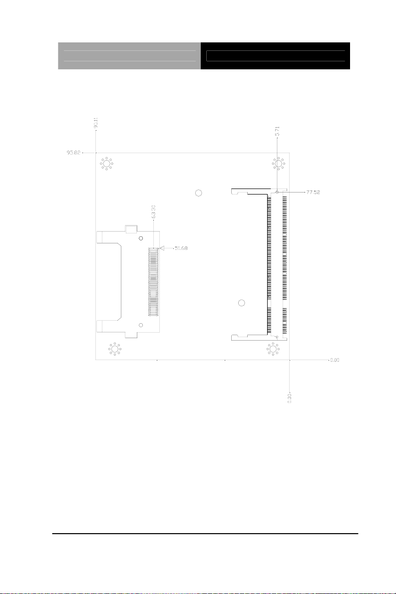
2.3 Mechanical Drawing
Component Side
Chapter 2 Quick Installation Guide 2- 5
Page 18
PC 104 CPU Module PFM-540I
Solder Side
Chapter 2 Quick Installation Guide 2 - 6
Page 19

PC 104 CPU Module PFM-540I
2.4 List of Jumpers
The board has a number of jumpers that allow you to configure your
system to suit your application.
The table below shows the function of each of the board's jumpers:
Jumpers
Label Function
JP1 CFD Master/Slave Selection
JP2 RS-232 Ring/5V Selection
JP3 LCD Clock Selection and Clear COMS
Chapter 2 Quick Installation Guide 2- 7
Page 20

PC 104 CPU Module PFM-540I
2.5 List of Connectors
The board has a number of connectors that allow you to configure
your system to suit your application. The table below shows the
function of each board's connectors:
Note: For further information about mating connectors, please refer
to the appendix of manual.
Connectors
Label Function
CN1 Front Panel Connector
CN2 PS2 Keyboard/Mouse Connector
CN3 Option Power Connector
CN4 USB Connector
CN5 VGA Display Connector
CN6 USB Connector
CN7 PC104 Connector
CN8
CN9
CN10
CN11 Floppy Connector
CN12 Power Connector
CN13 COM2 Connector
CN14
CN15
BAT1
Chapter 2 Quick Installation Guide 2 - 8
LPT Port Connector
IDE Connector
COM1 Connector
Ethernet Connector
LCD Connector
Battery Connector
Page 21

PC 104 CPU Module PFM-540I
CFD1 Type1 Compact Flash Slot
SODIMM1 DDR1 SODIMM Slot
2.6 Setting Jumpers
You configure your card to match the needs of your application by
setting jumpers. A jumper is the simplest kind of electric switch. It
consists of two metal pins and a small metal clip (often protected by
a plastic cover) that slides over the pins to connect them. To “close”
a jumper you connect the pins with the clip.
To “open” a jumper you remove the clip. Sometimes a jumper will
have three pins, labeled 1, 2 and 3. In this case you would connect
either pins 1 and 2 or 2 and 3.
3
2
1
Open C ed Closed 2-3los
OFF
ON ON 2-3
A pair of needle-nose pliers may be helpful when working with
jumpers.
If you have any doubts about the best hardware configuration for
your application, contact your local distributor or sales
representative before you make any change.
Generally, you simply need a standard cable to make most
connections.
Chapter 2 Quick Installation Guide 2- 9
Page 22

PC 104 CPU Module PFM-540I
2.7 CFD Master/Slave Selection (JP1)
JP1 Function
1-2 Slave
2-3 Master (Default)
2.8 RS-232 Ring/5V Selection (JP2)
JP2 Function
COM1
1-3 +5V
3-5 Ring (Default)
COM2
2-4 +5V
4-6 Ring (Default)
2.9 LCD Clock Selection and Clear CMOS (JP3)
JP3 Function
LCD Clock
1-3 Normal (Default)
3-5 Reverse
CMOS
2-4 Protected (Default)
Chapter 2 Quick Installation Guide 2 - 10
Page 23

PC 104 CPU Module PFM-540I
4-6 Clear
2.10 Front Panel Connector (CN1)
Pin Signal Pin Signal
1 Power LED (+) 2 Power LED (-)
3 N.C. 4 Speaker (+)
5
7 IDE LED(+) 8
9 N.C. 10 Reset(+)
11 Reset(-) 12 N.C.
13 Lan Speed LED(+) 14 Lan Speed LED(-)
15 Lan Active LED(+) 16 Lan Active LED(-)
17 N.C. 18 IrDA(+5V)
19 IrDA(N.C.) 20 IrDA(RX)
21
Speaker(-)
IrDA(GND)
6 N.C.
IDE LED(-)
22 IrDA(TX)
2.11 PS2 Keyboard/Mouse Connector (CN2)
Pin Signal Pin Signal
1 KB_DATA 2 KB_CLK
3
5 MS_DATA 6 MS_CLK
GND
4 +5V
Chapter 2 Quick Installation Guide 2- 11
Page 24

PC 104 CPU Module PFM-540I
2.12 Option Power Connector (CN3)
Pin Signal
1 -12V
2 -5V
3 GND
2.13 USB 3-4 Connector (CN4)
Pin Signal Pin Signal
1 +5V 2 GND
3 USBD3- 4 GND
5 USBD3+ 6 USBD4+
7 GND 8 USBD49 GND 10 +5V
2.14 VGA Display Connector (CN5)
Pin Signal Pin Signal
1 RED 2 +5V
3 GREEN 4 GND
5 BLUE 6 N.C.
7 N.C. 8 DDCDAT
9 GND 10 HSYNC
Chapter 2 Quick Installation Guide 2 - 12
Page 25

PC 104 CPU Module PFM-540I
11 GND 12 VSYNC
13 GND 14 DDCCLK
15 GND 16 GND
2.15 USB 1-2 Connector (CN6)
Pin Signal Pin Signal
1 +5V 2 GND
3 USBD1- 4 GND
5 USBD1+ 6 USBD2+
7 GND 8 USBD29 GND 10 +5V
2.16 PC 104 Connector (CN7)
As standard.
Note: PFM-540I does not support ISA card with DMA or Master mode in
PC/104 interface.
2.17 LPT Port Connector (CN8)
Pin Signal Pin Signal
1 #STROBE 2 #AFD
3 DATA0 4 #ERROR
Chapter 2 Quick Installation Guide 2- 13
Page 26

PC 104 CPU Module PFM-540I
5 DATA1 6 #INIT
7 DATA2 8 #SLIN
9 DATA3 10 GND
11 DATA4 12 GND
13 DATA5 14 GND
15 DATA6 16 GND
17 DATA7 18 GND
19 #ACK 20 GND
21 BUSY 22 GND
23
25 SELECT 26 N.C.
PE
24 GND
2.18 IDE Connector (CN9)
Pin Signal Pin Signal
1
3 DATA7 4
5 DATA6 6
7 DATA5 8
9 DATA4 10
11 DATA3 12
13 DATA2 14
15 DATA1 16
17 DATA0 18
Chapter 2 Quick Installation Guide 2 - 14
#RESET
2 GND
DATA8
DATA9
DATA10
DATA11
DATA12
DATA13
DATA14
DATA15
Page 27

PC 104 CPU Module PFM-540I
19 GND 20 N.C.
21 REQ 22 GND
23 #IOW 24 GND
25 #IOR 26 GND
27 IOREADY 28 GND
29 #DACK 30 GND
31 IRQ 32 N.C.
33 ADDR1 34 DETECT
35 ADDR0 36 ADDR2
37 #CS0 38 #CS1
39 HDDLED 40 GND
41 +5V 42 +5V
43 GND 44 N.C.
Note: The IDE interface on PFM-540I only supports two IDE devices. If
you use a CF card, there is only one IDE device usable.
2.19 COM1 Connector (CN10)
Pin Signal Pin Signal
1 DCD 2 RXD
3 TXD 4 DTR
5 GND 6 DSR
7 RTS 8 CTS
9 RI/5V 10 N.C.
Chapter 2 Quick Installation Guide 2- 15
Page 28

PC 104 CPU Module PFM-540I
2.20 Floppy Connector (CN11)
Pin Signal Pin Signal
1 GND 2
3 GND 4 N.C.
5 GND 6 N.C.
7 GND 8
9 GND 10 #MOTOR A
11 GND 12 #DRIVE SELECT B
13 GND 14 #DRIVE SELECT A
15 GND 16 #MOTOR B
17 GND 18 #DIR
19 GND 20 #STEP
21 GND 22 #WRITE DATA
23 GND 24 #WRITE GATE
25 GND 26 #TRACK0
27 GND 28 #WRITE PROTECT
29 N.C. 30 #READ DATA
31 GND 32 #HDSEL
#DENSEL
#INDEX
33 N.C. 34 #DISK CHANGE
Chapter 2 Quick Installation Guide 2 - 16
Page 29

PC 104 CPU Module PFM-540I
2.21 Power Connector (CN12)
Pin Signal Pin Signal
1 +5V 2 GND
3 GND 4 +12V
2.22 COM 2 Connector (CN13)
Pin Signal Pin Signal
1 DCD(485/422_TX-) 2
3 TXD(485/422_TX+) 4
5 GND 6
7 RTS 8
9 RI/5V 10
RXD(422_RX+)
DTR(422_RX-)
DSR
CTS
N.C.
2.23 Ethernet Connector (CN14)
Pin Signal Pin Signal
1 RX- 2
3 N.C. 4
5 CHASSIS_GND 6
7 N.C. 8
9
TX+
10
RX+
N.C.
CHASSIS_GND
N.C.
TX-
Chapter 2 Quick Installation Guide 2- 17
Page 30

PC 104 CPU Module PFM-540I
2.24 LCD Connector (CN15)
24-bit TTL
Pin Signal Pin Signal
1 +5V 2
3 GND 4
5 +3.3V 6
7 ENBKL 8
9 BLUE0
11 BLUE2
13 BLUE4
15 BLUE6
17
19
21
23
25 RED0
27 RED2
29 RED4
31 RED6
GREEN0 18 GREEN1
GREEN2 20 GREEN3
GREEN4 22 GREEN5
GREEN6 24 GREEN7
10 BLUE1
12 BLUE3
14 BLUE5
16 BLUE7
26 RED1
28 RED3
30 RED5
32 RED7
+5V
GND
+3.3V
GND
33 GND
35 CLOCK
37 DE
39 N.C.
Chapter 2 Quick Installation Guide 2 - 18
34 GND
36 VSYNC
38 HSYNC
40 ENAVEE
Page 31

PC 104 CPU Module PFM-540I
18-bit TTL
Pin Signal Pin Signal
1
3
5
7
9
11
13
15
17
19
21
23
25
27
29
31
+5V
GND
+3.3V
ENBKL
N.C 10 N.C
BLUE0 12 BLUE1
BLUE2 14 BLUE3
BLUE4 16 BLUE5
N.C 18 N.C
GREEN0 20 GREEN1
GREEN2 22 GREEN3
GREEN4 24 GREEN5
N.C 26 N.C
RED0 28 RED1
RED2 30 RED3
RED4 32 RED5
2
4
6
8
+5V
GND
+3.3V
GND
33
35
37
39
GND 34 GND
CLOCK 36 VSYNC
DE 38 HSYNC
N.C 40 ENAVEE
Chapter 2 Quick Installation Guide 2- 19
Page 32

PC 104 CPU Module PFM-540I
2.25 Battery Connector (BAT1)
Pin Signal Pin Signal
1 +3V 2
GND
2.26 DDR1 SODIMM Slot (SODIMM1 )
Standard SODIMM Slot
Note from AMD:
Memory configurations supported. Only one DIMM or SODIMM is
supported as long as the configuration requirements are met.
Devices Max Memory1Max GLIU
Frequency
4 512M 400MHz
8 1G 400MHz
4 512M 333MHz
8 1G 333MHz
16 2G 333MHz
1: Maximum memory is assuming 1Gbit devices.
GLCP 4C00000Fh
Upper Bits/Lower Bits
F2F100FFh/ 56960004h
F2F100FFh/ 56960004h
F2F100FFh/ 56960004h
F2F100FFh/ 56960004h
F2F100FFh/ 56960004h
GLMC
2000001 Ah
Bits【26:24】
4
4
3
3
3
Chapter 2 Quick Installation Guide 2 - 20
Page 33

PC 104 CPU Module PFM-540I
Chapter
3
Award
BIOS Setup
Chapter 3 Award BIOS Setup 3-1
Page 34

PC 104 CPU Module PFM-540I
3.1 System Test and Initialization
These routines test and initialize board hardware. If the
routines encounter an error during the tests, you will either
hear a few short beeps or see an error message on the
screen. There are two kinds of errors: fatal and non-fatal. The
system can usually continue the boot up sequence with
non-fatal errors. Non-fatal error messages usually appear on
the screen along with the following instructions:
Press <F1> to RESUME
Write down the message and press the F1 key to continue
the boot up sequence.
System configuration verification
These routines check the current system configuration
against the values stored in the CMOS memory. If they do
not match, the program outputs an error message. You will
then need to run the BIOS setup program to set the
configuration information in memory.
There are three situations in which you will need to change
the CMOS settings:
1. You are starting your system for the first time
2. You have changed the hardware attached to your system
3. The CMOS memory has lost power and the configuration
information has been erased.
The PFM-540I CMOS memory has an integral lithium battery
backup for data retention. However, you will need to replace
the complete unit when it finally runs down.
Chapter 3 Award BIOS Setup 3-2
Page 35

PC 104 CPU Module PFM-540I
3.2 Award BIOS Setup
Awards BIOS ROM has a built-in Setup program that allows
users to modify the basic system configuration. This type of
information is stored in battery-backed CMOS RAM so that it
retains the Setup information when the power is turned off.
Entering Setup
Power on the computer and press <Del> immediately. This
will allow you to enter Setup.
Standard CMOS Features
Use this menu for basic system configuration. (Date, time,
IDE, etc.)
Advanced BIOS Features
Use this menu to set the advanced features available on your
system.
Chapter 3 Award BIOS Setup 3-3
Page 36

PC 104 CPU Module PFM-540I
Advanced Chipset Features
Use this menu to change the values in the chipset registers
and optimize your system performance.
Integrated Peripherals
Use this menu to specify your settings for integrated
peripherals. (Primary slave, secondary slave, keyboard,
mouse etc.)
Power Management Setup
Use this menu to specify your settings for power
management. (HDD power down, power on by ring, KB wa ke
up, etc.)
PnP/PCI Configurations
This entry appears if your system supports PnP/PCI.
PC Health Status
This menu allows you to set the shutdown temperature for
your system.
Frequency/Voltage Control
Use this menu to specify your settings for auto detect
DIMM/PCI clock and spread spectrum.
Load Fail-Safe Defaults
Use this menu to load the BIOS default values for the
minimal/stable performance for your system to operate.
Chapter 3 Award BIOS Setup 3-4
Page 37

PC 104 CPU Module PFM-540I
Load Optimized Defaults
Use this menu to load the BIOS default values that are
factory settings for optimal performance system operations.
While AWARD has designated the custom BIOS t o maximize
performance, the factory has the right to change these
defaults to meet their needs.
Set Supervisor/User Password
Use this menu to set Supervisor/User Passwords.
Save and Exit Setup
Save CMOS value changes to CMOS and exit setup.
Exit Without Saving
Abandon all CMOS value changes and exit setup.
You can refer to the “ AAEON BIOS Item
Description.pdf” file in the CD for the meaning of each
setting in this chapter.
Chapter 3 Award BIOS Setup 3-5
Page 38

PC 104 CPU Module PFM-540I
Chapter
4
Driv
Installation
Chapter 4 Driver Installation 4 - 1
er
Page 39

PC 104 CPU Module PFM-540I
4.1 Software Drivers
This chapter describes the operation and installation of the display
drivers supplied on the Supporting CD-ROM that are shipped with
your product. The onboard VGA adapter is based on the AMD LX
VGA Flat Panel/CRT controller. This controller offers a large set of
extended functions and higher resolutions. The purpose of the
enclosed software drivers is to take advantage of the extended
features of the AMD LX VGA Flat Panel/CRT controller.
Hardware Configuration
Some of the high-resolution drivers provided in this package will
work only in certain system configurations. If a driver does not
display correctly, try the following:
1. Change the display controller to CRT-only mode, rather than flat
panel or simultaneous display mode. Some high-resolution
drivers will display correctly only in CRT mode.
2. If a high-resolution mode does not support your system, try to
use a lower-resolution mode. For example, 1024 x 768 mode will
not work on some systems, but 800 x 600 mode supports the
most.
Chapter 4 Driver Installation 4 - 2
Page 40

PC 104 CPU Module PFM-540I
4.2 Necessary to Know
The instructions in this manual assume that you understand
elementary concepts of MS-DOS and the IBM Personal Computer.
Before you attempt to install any driver from the Supporting
CD-ROM, you should:
Know how to copy files from a CD-ROM to a directory on the
hard disk
Understand the MS-DOS directory structure
If you are uncertain about any of these concepts, please refer
to the DOS or OS/2 user reference guides for more
information before you proceed with the installation.
Before you begin
The Supporting CD-ROM contains different drivers for
corresponding Windows OS, please choose the specific driver for
your Windows OS.
Chapter4 Drivers Installation 4 - 3
Page 41

PC 104 CPU Module PFM-540I
4.3 Installing VGA Driver
Win XP / Win XPe VGA
Place the Driver CD-ROM into your CD-ROM drive and follow the
steps below to install.
1. Click on Start button.
2. Click on Settings button.
3. Click on Control Panel button.
4. Click on System button.
5. Select Hardware and click on Device Manager….
6. Double click on Video Controller (VGA Compatible).
7. Click on Update Driver….
8. Click on Next.
9. Select Search for a suitable driver…, then click on Next.
10. Select Specify a location, then click on Next.
11. Click on Browse.
12. Select “lx_win” file from CD-ROM (Drivers/Step 1 –
LX_Graphics) then click on Open.
13. Click on OK.
14. Click on Next.
15. Click on Yes.
16. Click on Finish.
Note: The user must install this system driver before install other
device drivers.
Chapter 4 Driver Installation 4 - 4
Page 42

PC 104 CPU Module PFM-540I
4.4 Installing AES Driver
Win XP / Win XPe Geode LX AES Crypto
Place the Driver CD-ROM into your CD-ROM drive and follow the
steps below to install.
1. Click on Start button.
2. Click on Settings button.
3. Click on Control Panel button.
4. Click on System button.
5. Select Hardware and click on Device Manager….
6. Double click on Entertainment Encryption/Decryption
Controller.
7. Click on Update Driver….
8. Click on Next.
9. Select Search for a suitable driver…, then click on Next.
10. Select Specify a location, then click on Next.
11. Click on Browse.
12. Select “GeodeLX_XP_WDM_AES_v2.01.00” file from
CD-ROM (Driver/Step 2 – AES) then click on Open.
13. Click on OK.
14. Click on Next.
15. Click on Yes.
16. Click on Finish.
Chapter4 Drivers Installation 4 - 5
Page 43

PC 104 CPU Module PFM-540I
4.5 Installing PCI to ISA Bridge Driver
Win XP / Win XPe System
Place the Driver CD-ROM into your CD-ROM drive and follow the
steps below to install.
1. Click on Start button.
2. Click on Settings button.
3. Click on Control Panel button.
4. Click on System button.
5. Select Hardware and click on Device Manager….
6. Double click on Other PCI Bridge Device
7. Click on Update Driver….
8. Click on Next.
9. Select Search for a suitable driver…, then click on Next.
10. Select Specify a location, then click on Next.
11. Click on Browse.
12. Select “Ite” file from CD-ROM (Drivers/Step 3 – PCI to ISA
Bridge) then click on open.
13. Click on OK.
14. Click on Next.
15. Click on Finish.
Chapter 4 Driver Installation 4 - 6
Page 44

PC 104 CPU Module PFM-540I
4.6 Installing Ethernet Driver
1. Click on the Step 4 –Install Lan folder.
2. Double click on the Setup file located in the folder.
3. Follow the instructions that the window shows.
4. The system will help you install the driver automatically.
4.7 Ethernet Software Configuration
The onboard Ethernet interface supports all major network
operating systems. I/O addresses and interrupts are easily
configured via the Insyde BIOS Setup. To configure the medium
type, to view the current configuration, or to run diagnostics, please
refer to the following instruction:
1. Power the main board on. Ensure that the RSET8139.EXE file
is located in the working drive.
2. At the prompt, type RSET8139.EXE and press <ENTER>.
The Ethernet configuration program will then be displayed.
3. This simple screen shows all the available options for the
Ethernet interface. Just highlight the option you wish to
change by using the Up and DOWN keys. To change a
selected item, press <ENTER>, and a screen will appear with
the available options. Highlight your option and press
<ENTER>. Each highlighted option has a helpful message
Chapter4 Drivers Installation 4 - 7
Page 45

PC 104 CPU Module PFM-540I
guide displayed at the bottom of the screen for additional
information.
4. After you have made your selections and the configuration is
what you want, press <ESC>. A prompt will appear asking if
you want to save the configuration. Press "Y" if you want to
save.
There are three very useful diagnostic functions offered in the
Ethernet Setup Menu as follows:
1. Run EEPROM test
2. Run Diagnostics on Board
3. Run Diagnostics on Network
Each option has its own display screen, which shows the format
and result of any diagnostic tests undertaken.
Chapter 4 Driver Installation 4 - 8
Page 46

PC 104 CPU Module PFM-540I
A
Programming the
Watchdog Timer
Appendix
Appendix A Programming the Watchdog Timer A-1
Page 47

PC 104 CPU Module PFM-540I
A.1 Programming
PFM-540I utilizes IT8712F-A chipset as its watchdog timer
controller.
Below are the procedures to complete its configuration and the
AAEON intial watchdog timer program is also attached based on
which you can develop customized program to fit your application.
Configuring Sequence Description
After the hardware reset or power-on reset, the IT8712F-A enters
the normal mode with all logical devices disabled except KBC. The
initial state (enable bit ) of this logical device (KBC) is determined
by the state of pin 121 (DTR1#) at the falling edge of the system
reset during power-on reset.
Appendix A Programming the Watchdog Ti mer A-2
Page 48

PC 104 CPU Module PFM-540I
There are three steps to complete the configuration setup: (1) Enter
the MB PnP Mode; (2) Modify the data of configuration registers; (3)
Exit the MB PnP Mode. Undesired result may occur if the MB PnP
Mode is not exited normally.
(1) Enter the MB PnP Mode
To enter the MB PnP Mode, four special I/O write operations are to
be performed during Wait for Key state. To ensure the initial state of
the key-check logic, it is necessary to perform four write opera -tions
to the Special Address port (2EH). Two different enter keys are
provided to select configuration ports (2Eh/2Fh) of the next step.
(2) Modify the Data of the Registers
All configuration registers can be accessed after entering the MB
PnP Mode. Before accessing a selected register, the content of
Index 07h must be changed to the LDN to which the register
belongs, except some Global registers.
(3) Exit the MB PnP Mode
Set bit 1 of the configure control register (Index=02h) to 1 to exit the
MB PnP Mode.
Appendix A Programming the Watchdog Timer A-3
Page 49

PC 104 CPU Module PFM-540I
WatchDog Timer Configuration Registers
Configure Control (Index=02h)
This register is write only. Its values are not sticky; that is to say, a
hardware reset will automatically clear the bits, and does not
require the software to clear them.
WatchDog Timer Control Register (Index=71h, Default=00h)
Appendix A Programming the Watchdog Ti mer A-4
Page 50

PC 104 CPU Module PFM-540I
WatchDog Timer Configuration Register (Index=72h,
Default=00h)
WatchDog Timer Time-out Value Register (Index=73h,
Default=00h)
Appendix A Programming the Watchdog Timer A-5
Page 51

PC 104 CPU Module PFM-540I
A.2 IT8712F-A Watchdog Timer Initial Program
.MODEL SMALL
.CODE
Main:
CALL Enter_Configuration_mode
CALL Check_Chip
mov cl, 7
call Set_Logic_Device
;time setting
mov cl, 10 ; 10 Sec
dec al
Watch_Dog_Setting:
;Timer setting
mov al, cl
mov cl, 73h
call Superio_Set_Reg
;Clear by keyboard or mouse interrupt
mov al, 0f0h
mov cl, 71h
call Superio_Set_Reg
;unit is second.
mov al, 0C0H
mov cl, 72h
call Superio_Set_Reg
Appendix A Programming the Watchdog Ti mer A-6
Page 52

PC 104 CPU Module PFM-540I
; game port enable
mov cl, 9
call Set_Logic_Device
Initial_OK:
CALL Exit_Configuration_mode
MOV AH,4Ch
INT 21h
Enter_Configuration_Mode PROC NEAR
MOV SI,WORD PTR CS:[Offset Cfg_Port]
MOV DX,02Eh
MOV CX,04h
Init_1:
MOV AL,BYTE PTR CS:[SI]
OUT DX,AL
INC SI
LOOP Init_1
RET
Enter_Configuration_Mode ENDP
Exit_Configuration_Mode PROC NEAR
MOV AX,0202h
CALL Write_Configuration_Data
Appendix A Programming the Watchdog Timer A-7
Page 53

PC 104 CPU Module PFM-540I
RET
Exit_Configuration_Mode ENDP
Check_Chip PROC NEAR
MOV AL,20h
CALL Read_Configuration_Data
CMP AL,87h
JNE Not_Initial
MOV AL,21h
CALL Read_Configuration_Data
CMP AL,12h
JNE Not_Initial
Need_Initial:
STC
RET
Not_Initial:
CLC
RET
Check_Chip ENDP
Read_Configuration_Data PROC NEAR
MOV DX,WORD PTR CS:[Cfg_Port+04h]
OUT DX,AL
Appendix A Programming the Watchdog Ti mer A-8
Page 54

PC 104 CPU Module PFM-540I
MOV DX,WORD PTR CS:[Cfg_Port+06h]
IN AL,DX
RET
Read_Configuration_Data ENDP
Write_Configuration_Data PROC NEAR
MOV DX,WORD PTR CS:[Cfg_Port+04h]
OUT DX,AL
XCHG AL,AH
MOV DX,WORD PTR CS:[Cfg_Port+06h]
OUT DX,AL
RET
Write_Configuration_Data ENDP
Superio_Set_Reg proc near
push ax
MOV DX,WORD PTR CS:[Cfg_Port+04h]
mov al,cl
out dx,al
pop ax
inc dx
out dx,al
ret
Superio_Set_Reg endp.Set_Logic_Device proc near
Set_Logic_Device proc near
Appendix A Programming the Watchdog Timer A-9
Page 55

PC 104 CPU Module PFM-540I
push ax
push cx
xchg al,cl
mov cl,07h
call Superio_Set_Reg
pop cx
pop ax
ret
Set_Logic_Device endp
;Select 02Eh->Index Port, 02Fh->Data Port
Cfg_Port DB 087h,001h,055h,055h
DW 02Eh,02Fh
END Main
Note: Interrupt level mapping
0Fh-Dh: not valid
0Ch: IRQ12
.
.
03h: IRQ3
02h: not valid
01h: IRQ1
00h: no interrupt selected
Appendix A Programming the Watchdog Ti mer A-10
Page 56

PC 104 CPU Module PFM-540I
I/O Information
Appendix
B
Appendix B I/O Information B - 1
Page 57

PC 104 CPU Module PFM-540I
B.1 I/O Address Map
Appendix B I/O Information B - 2
Page 58

PC 104 CPU Module PFM-540I
B.2 1st MB Memory Address Map
Appendix B I/O Informaion B - 3
Page 59

PC 104 CPU Module PFM-540I
B.3 IRQ Mapping Chart
B.4 DMA Channel Assignments
Appendix B I/O Information B - 4
Page 60

PC 104 CPU Module PFM-540I
x Appendi
Mating Connecotor
C
Appendix C Mating Connector C - 1
Page 61

PC 104 CPU Module PFM-540I
C.1 List of Mating Connectors and Cables
The table notes mating connectors and available cables.
Connector
Label
CN1
CN2
CN3
CN4
CN5
Function
Front
Panel
Connector
PS2
Keyboard/
Mouse
Connector
Option
Power
Connector
USB
Connector
VGA
Display
Mating Connector
Vendor Model no
Neltron
Neltron
Dupont
Neltron
Neltron
2226A-XX N/A
2026B--XX Keyboard & Mouse
2541-1H
2026B--XX USB Cable
2026B--XX CRT Cable
Available Cable AAEON Cable
P/N
1700060152
Cable
N/A
1709100201
1701160201
Connector
CN6
CN8
Appendix C Mating Connector C - 2
USB
Connector
LPT Port
Connector
Neltron
Keentop
2026B--XX USB Cable
1014
Series
Parallel Port Cable
1709100201
1701260201
Page 62

CN9
CN10
CN11
CN12
PC 104 CPU Module PFM-540I
IDE
Connector
COM1
Connector
Floppy
Connector
Power
Keentop
1014
IDE Cable
1701440350
Series
Keentop
1014
Serial Port Cable
1701100207
Series
Keentop
1014
Series
Floppy Disk Drive
Cable
1701340703
Ever 2542H-04 N/A
Connector
CN13
COM2
Connector
CN14
Ethernet
Connector
CN15
LCD
Connector
BAT1 Battery
Connector
Keentop
1014
Serial Port Cable
1701100207
Series
Keentop
1014
Ethernet Cable
1700100200
Series
HO TIEN 1255H N/A
HRS DF14-MS-1
N/A
.25C
Appendix C Mating Connector C - 3
 Loading...