

Page 1
99IoT (Shenzhen) Co., Ltd.
User_Manual
User Manual of AF-W12xTx Wi-Fi Module
1
/ 12
For more details, please visit www.sz99iot.com
Design Manual of AF-W12xTx Module Hardware
1.2 Basic characteristics of module...........................................................................2
1.3 Module type ........................................................................................................2
1.5 Block diagram of hardware.................................................................................4
2.2 Reset pin..............................................................................................................5
2.3 Reference circuit design......................................................................................6
6.2 Directions for module layout ............................................................................10
V1.1 2017.08
Contents
1 Introduction...............................................................................................................2
1.1 Abstract ............................................................................................................... 2
1.4 Sketch map of module.........................................................................................3
2 Design issues of hardware ........................................................................................ 5
2.1 Power design .......................................................................................................5
3 Application programming interface..........................................................................7
4 Log serial port ...........................................................................................................8
5 Communication serial port........................................................................................9
6 RF design and layout issues......................................................................................9
6.1 RF selecting resistor.......................................................................................... 9
6.3 Advice on module layout ..................................................................................11
7 Purchase and support ..............................................................................................12
Patent statements
2017 99 IoT (Shenzhen) Co., Ltd. reserves all rights for this document. Any part of the
document is not allowed to be reproduced, stored in any retrieval system or transmitted in any
form that has not been unified in written form by 99 IoT (Shenzhen) Co., Ltd.
Page 2
99IoT (Shenzhen) Co., Ltd.
User_Manual
User Manual of AF-W12xTx Wi-Fi Module
2
/ 12
For more details, please visit www.sz99iot.com
1 Introduction
Supporting Simple Configuration intelligent networking function (APP is provided)
Supporting Amazon, Baidu cloud, Jingdong cloud, Ali cloud
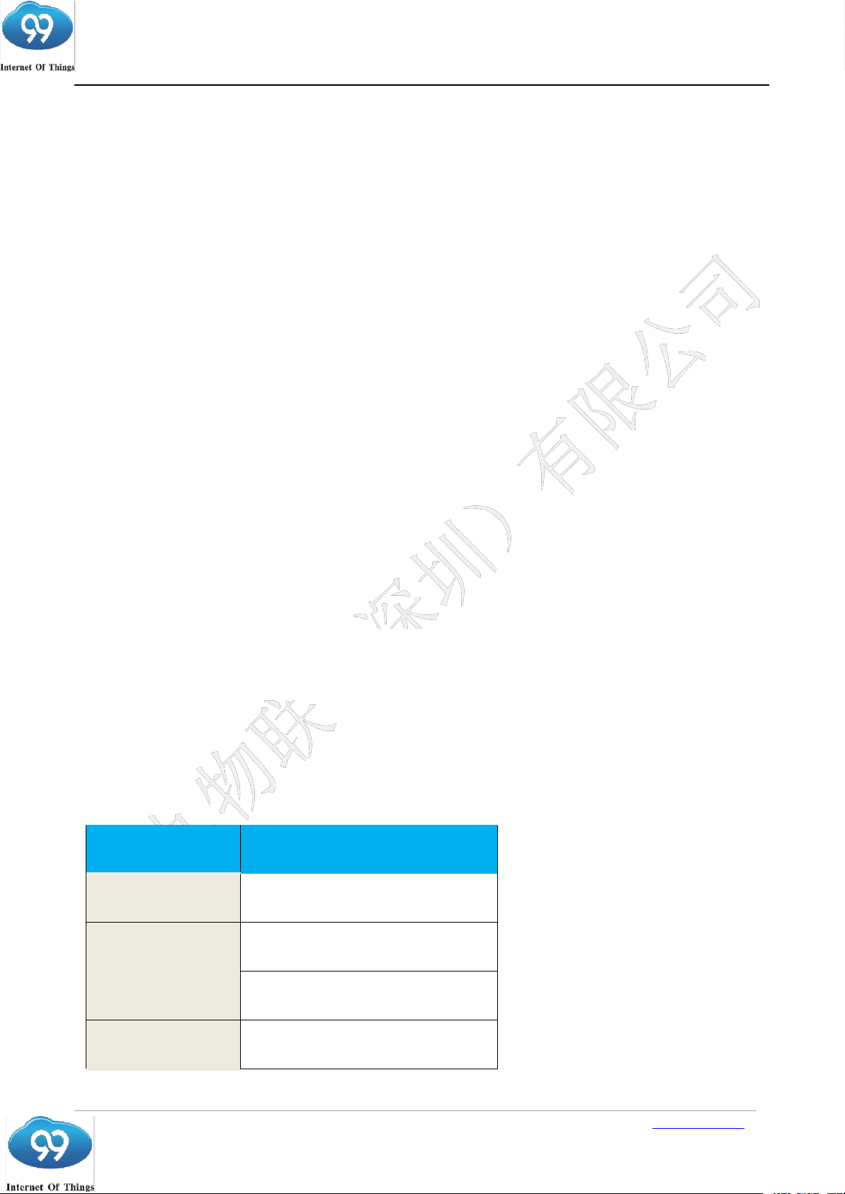
Module name
Module description
AF-W121TI
PCB onboard antenna
AF-W121TO
IPEX outer antenna (optional)
AF-W123TI
PCB onboard antenna
AF-W123TO
IPEX outer antenna (optional)
1.1 Abstract
The document mainly lists the issues that need attention in all stages during the use of
99 IoT Wi-Fi module AF-W12xTx design by users in order to reduce design costs and
increase product stability as far as possible.
AF-W12xTx is a complete and self-contained WiFi network solution module that can
run either in MCU+WIFI mode or as a slave on other master MCU. The sensor and
other applied specific devices can be integrated through GPIO port.
1.2 Basic characteristics of module
Standard: 802.11 b/g/n 1x1
Working mode: STA, AP, STA+AP
Complete IoT solution (SDK, Cloud service, APP)
Each module has unique global MAC ID
Antenna: outer antenna, IPEX antenna interface, onboard antenna
Working ambient temperature: -20 to 85℃
1.3 Module type
Page 3
99IoT (Shenzhen) Co., Ltd.
User_Manual
User Manual of AF-W12xTx Wi-Fi Module
3
/ 12
For more details, please visit www.sz99iot.com
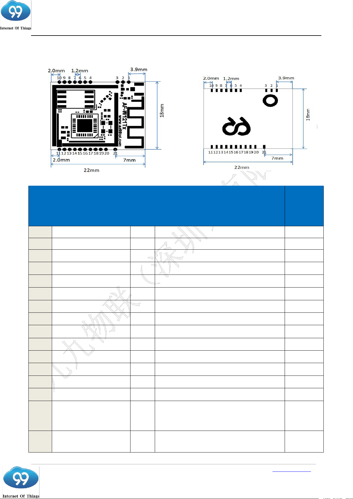
1.4
引脚 名称 /主功能 类型 可选功能
Pin Name/ main function Type Optional functions
其它功能
Other
functions
1
GND
2
Wi-Fi-ANTENA
3
GND
4
NC/GND
5
CHIP_EN(RESET)
I
Reset
6
GPIOA_14
I/O
PWM0/ SWD_CLK
7
GPIOA_15
I/O
PWM1/ SWD_DATA
8
GPIOA_0
I/O
PWM2/EXT_32K/WL_LED
9
GPIOA_12
I/O
PWM3
10
GND
11
VDD33
12
GND
13
VBAT_MEAS
14
GPIOA_5
I/O
SDIO_SIDEBAND_INT/ PWM4
15
GPIOA_18
I/O
UART0_RXD/SPI1_CLK /SPI0_CLK
I2C1_SCL /
/
SD_D2/ TIMER4_TRIG/
I2S_MCK
16
GPIOA_19
I/O
UART0_CTS/SPI1_CS/SPI0_CS
I2C0_SDA/SD_D3/TIMER5_TRIG
I2S_SD_TX
Sketch map of module
Page 4
99IoT (Shenzhen) Co., Ltd.
User_Manual
User Manual of AF-W12xTx Wi-Fi Module
4
/ 12
For more details, please visit www.sz99iot.com
17
GPIOA_22
I/O
UART0_RTS / SPI1_MISO/
SPI0_MISO / I2C0_SCL
SD_D0 / PWM5 / I2S_WS
18
GPIOA_23
I/O
UART0_TXD/ SPI1_MOSI/
SPI0_MOSI / I2C1_SDA
SD_D1 / PWM0
19
GPIOA_30
I/O
UART2_Log_TXD/ I2C0_SDA/
PWM3 / RTC_OUT
20
GPIOA_29
I/O
UART2_Log_RXD / I2C0_SCL
PWM4
21
GND
Note:
1.5
Block diagram of hardware
AF-W121Tx/AF-W
123Tx
Backup register forpower
save SRAM16B
P
MU
3.3V
Inp
ut
256
K
SRA
M
ARMCM4F-M
CU
125MHZ ormor
e
512
K
R
OM
Digit
al
Sensor
ExternalFLAS
H
2M(Upto
128M
)
GDM
A
12
VBAT_MEA
GTIMER
6set
s
SPI
Master/Salve
I2C
Master/Salve
SDIO/USB
Device
SoC
ON
2.4G
HZ
S
witch
Bus
WIFI-802.11b/
g/nMAC
GPIOs *
11
PWM *
6
I2S
RTC
SW
D
UART *
2
ADC
AP
/
CloudServer
1. PIN19, 20 are for the use when Wi-Fi debugs LOG information input and output
port.
2. PIN19 of module AF-W121Tx needs to be pulled up to 3.3V externally, or floating,
or to ensure that power-on time isn’t low level.
3. Please keep CHIP_EN or other pins floating if they are not used.
Page 5

99IoT (Shenzhen) Co., Ltd.
User_Manual
User Manual of AF-W12xTx Wi-Fi Module
5
/ 12
For more details, please visit www.sz99iot.com
2 Design issues of hardware
(1)Input pin of main power supply is [PIN11], module supply voltage is DC 3.0~3.6, filter
capacitor of 4.7-10uF needs to be placed near its location; loading capability of 3.3V
(4)[PIN13] is ADC input pin, which can be used to detect battery voltage.
(1) [PIN5] is module reset pin: CHIP_EN(RESET), needs to be pulled up by connecting
resistor of 100KΩ to power supply of 3.3V. The module will be in shutdown mode for
low level.
(3) If other MCU is needed to reset-control the module through the pin, a low pulse signal is
【ONSEMI/MAX809STR/SOT23/LM1117-3.3】. It can also be monitored by other
2.1 Power design
As shown in Figure 1.4 above
power supply, the power supply with rated output current ≥500mA is recommended.
(2)Use of DC/DC powerchip: voltage output meets 3.3V and the maximum current output
meets 500mA, input capacitor is as close as possible to voltage input pin, thickening
ground wire width or grounded copper area, punching more via holes for different layers.
(3)For LDO design, the voltage output meets 3.3V and the maximum current output meets
500mA, paying attention to device junction temperature, the formula of power
consumption is PD=(Vin-Vout) * Iload + Vin * IGND, in which Vin is input voltage,
Vout is output voltage, Iload is load current, IGND is ground current.
Reset PIN
2.2
As shown in Figure 1.4 above
( 2 ) If the module is not controlled by other MCU, the decoupling capacitor of 100nF is
recommended to be added near its location to enhance the stability of the system.
needed and the duration of low level is at least 10ms.
(4) If the voltage of power supply is unstable (lower than 3.0V), it may cause module halt.
It is recommended to add Brown out reset circuit, and the recommended chip is as
follows:
(master control) MCU.
Page 6

99IoT (Shenzhen) Co., Ltd.
User_Manual
User Manual of AF-W12xTx Wi-Fi Module
6
/ 12
For more details, please visit www.sz99iot.com
2.3 Reference circuit design
Reference circuit design of module AF-W121Tx/AF-W123Tx, 5V to 3.3V conversion
5V to 3.3V conversion, LDO reference circuit design
Reset reference circuit design
Page 7

99IoT (Shenzhen) Co., Ltd.
User_Manual
User Manual of AF-W12xTx Wi-Fi Module
7
/ 12
For more details, please visit www.sz99iot.com
UART level switching circuit
Default: R64, UART 3V3 IO
UART T/RX
when UART T/R
3 Application programming interface
(3) The module uses SWD port for programming debugging, the PINs (module PIN6, 7)
LED flashes when
The pin will pull low up
(1) Users can use simulation tool and build environment for debugging.
(2) SWD port can be used to achieve DPA programming (master computer software does not
open temporarily).
need to be connected are shown in following figure:
Page 8

99IoT (Shenzhen) Co., Ltd.
User_Manual
User Manual of AF-W12xTx Wi-Fi Module
8
/ 12
For more details, please visit www.sz99iot.com
Log serial port
(3) Serial port pinboard is used to achieve AT Conmand operation by connecting
(4) Serial port pinboard is used to achieve firmware programming by connecting
abovementioned PIN.
4
(1) PIN19 is a boot PIN:
Level Function
0 Download image from UART
1 Boot from Flash
(2) Serial port pinboard is used to observe output log by connecting abovementioned PIN to
find abnormity of module software conveniently.
abovementioned PIN.
Page 9

99IoT (Shenzhen) Co., Ltd.
User_Manual
User Manual of AF-W12xTx Wi-Fi Module
9
/ 12
For more details, please visit www.sz99iot.com
5 Communication serial port
6.1 RF selecting resistor
R4
R3
R5
R5 selects onboard antenna.
In general, it is recommended to communicate with other MCU through this serial port,
the pins which need to be connected are shown in following figure: [PIN16], [PIN17]
are optional. These two pins are used to achieve fluid control.
6 RF design and layout issues
Selecting RF antenna through
above selection of 0Ω resistor:
R3 selects [pin5] RF pin;
R4 selects IPEX outer antenna
pedestal;
Page 10

99IoT (Shenzhen) Co., Ltd.
User_Manual
User Manual of AF-W12xTx Wi-Fi Module
10
/ 12
For more details, please visit www.sz99iot.com
6.2 Directions for module layout
(2) The module must be placed vertically with the onboard antenna top located
layout forbidden area.
(1) When using onboard antenna, layout forbidden area is seen in the figure
below;
or the module is placed horizontally with component side up;
(3) When the module is placed vertically, the clear height of module’s both
sides is at least over 12mm;
When the module is placed horizontally, the clear height under the module is
over 6mm;
Cable and other metals are prohibited above the module;
(4) Neither can copper be cladded nor can metal devices, sensors, interference
sources or other materials that have an impact on signal be placed under the
Layout forbidden area
Page 11

99IoT (Shenzhen) Co., Ltd.
User_Manual
User Manual of AF-W12xTx Wi-Fi Module
11
/ 12
For more details, please visit www.sz99iot.com
Layout forbidden area
Layout forbidden area
6.3 Advice on module layout
PCB is hollowed under the antenna.
12mm
2mm
Layout forbidden area
12mm
2mm
2mm
12
m
m
Layout forbidden area
2
m
12mm
When users use the module with onboard PCB antenna, they can put the module in the
following areas of the baseboard, or place the antenna of module outside the
baseboard, so the module onboard antenna has a larger clearance area compared to the
bottom to reduce the impact of metal devices on PCB antenna and wireless signals. Or
Page 12

99IoT (Shenzhen) Co., Ltd.
User_Manual
User Manual of AF-W12xTx Wi-Fi Module
12
/ 12
For more details, please visit www.sz99iot.com
Updating description of historical versions
Revision
Release Data
Summary
V1.0
2017/03/10
First draft
V1.1
2017/08/15
Adding module layout description,
firmware download description
Created by: Frank Wong
Date:8/15/2017
7 Purchase and support
Tel. 0755-88602663
E-mail: sales@sz99iot.com
Frank@sz99iot.com
Address: 609C north block, Cangsong Building, Tairan Seven Road, Futian District, Shenzhen
Website: www.sz99iot.com
*RF warning for Mobile device:
This equipment complies with FCC radiation exposure limits set forth for an uncontrolled environment. This equipment
should be installed and operated with minimum distance 20cm between the radiator & your body.
§ 15.19 Labelling requirements.
This device complies with part 15 of the FCC Rules. Operation is subject to the following two conditions: (1) This
device may not cause harmful interference, and (2) this device must accept any interference received, including
interference that may cause undesired operation.
§ 15.21 Information to user.
Any Changes or modifications not expressly approved by the party responsible for compliance could void
the user's authority to operate the equipment.
Page 13

99IoT (Shenzhen) Co., Ltd.
User_Manual
User Manual of AF-W12xTx Wi-Fi Module
13
/ 12
For more details, please visit www.sz99iot.com
§ 15.105 Information to the user.
Note: This equipment has been tested and found to comply with the limits for a
Class B digital device, pursuant to part 15 of the FCC Rules. These limits are designed to provide reasonable
protection against harmful interference in a residential installation. This equipment generates uses and can
radiate radio frequency energy and, if not installed and used in accordance with the instructions, may cause
harmful interference to radio communications. However, there is no guarantee that interference will not occur
in a particular installation. If this equipment does cause harmful interference to radio or television reception,
which can be determined by turning the equipment off and on, the user is encouraged to try to correct the
interference by one or more of the following measures:
-Reorient or relocate the receiving antenna.
-Increase the separation between the equipment and receiver.
-Connect the equipment into an outlet on a circuit different from that to which the receiver is connected.
-Consult the dealer or an experienced radio/TV technician for help.
 Loading...