

4D systems gen4-uLCD-50D-SB, gen4-uLCD-50D, gen4-uLCD-50D-AR, gen4-uLCD-50DT-PI, gen4-uLCD-50D-CLB Datasheet
...Page 1
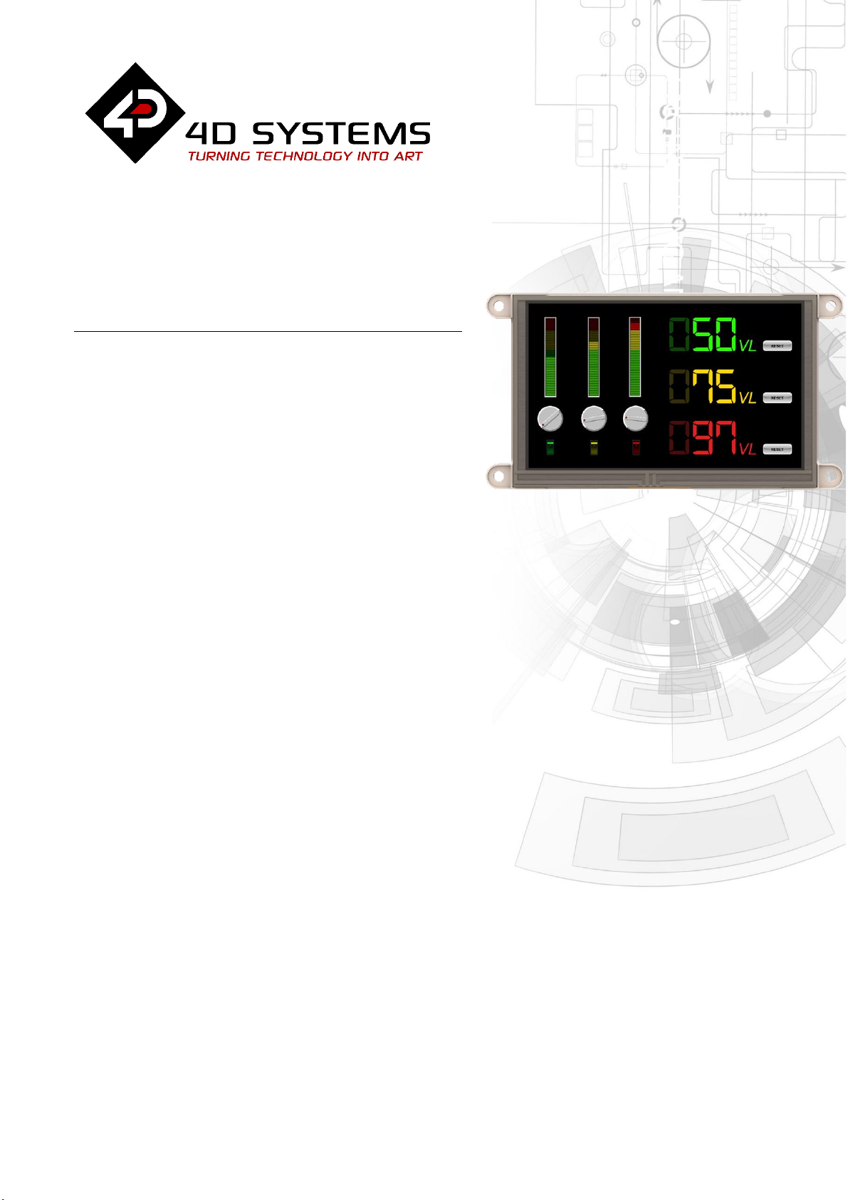
gen4-uLCD-50D (Non-touch)
gen4-uLCD-50DT (Resistive touch)
gen4-uLCD-50D-CLB (Non-touch w/ CLB)
gen4-uLCD-50DCT-CLB (Capacitive touch w/CLB)
gen4-uLCD-50Dxx-xxx-SB (Super Bright variants)
W W W . 4 D S Y S T E M S . C O M . A U
gen4-HMI Display Module Series
DATASHEET
DOCUMENT DATE: 05th AUGUST 2019
DOCUMENT REVISION: 1.8
Uncontrolled Copy when printed or downloaded.
Please refer to the 4D Systems website for the latest
Revision of this document
Page 2
Table of Contents
Table of Contents
1. Description ...................................................................................................................4
2. Features .......................................................................................................................4
3. Hardware Overview ......................................................................................................5
4. Hardware Interface - Pins ..............................................................................................7
4.1. Serial Ports – TTL Level Serial ......................................................................................7
4.2. General Purpose I/O ...................................................................................................8
4.3. System Pins ................................................................................................................9
4.4. Alternate Pin Function Overview ................................................................................9
4.5. SPI ..............................................................................................................................10
4.6. I2C ..............................................................................................................................10
4.7. Pulse Out ....................................................................................................................11
4.8. PWM Out ....................................................................................................................11
4.9. Pin Counter.................................................................................................................11
4.10. Quadrature In .............................................................................................................12
4.11. Analog Inputs .............................................................................................................12
5. Module Features ........................................................................................................ 13
5.1. DIABLO16 Processor ...................................................................................................13
5.2. Audio ..........................................................................................................................13
5.3. SD/SDHC Memory Cards .............................................................................................13
5.4. FAT16 .........................................................................................................................13
5.5. Application PCB Support .............................................................................................14
5.6. RF / EMI Shielding Support .........................................................................................14
6. Display/Module Precautions ....................................................................................... 15
7. Hardware Tools .......................................................................................................... 15
7.1. 4D Programming Cable/Adaptor .................................................................................15
8. Software Overview - Language .................................................................................... 16
9. 4D Systems - Workshop 4 IDE ...................................................................................... 17
9.1. Workshop4 - Designer ................................................................................................17
9.2. Workshop4 – ViSi........................................................................................................17
9.3. Workshop4 – ViSi Genie..............................................................................................18
9.4. Workshop4 – Serial .....................................................................................................18
9.5. PmmC/Firmware Programming ..................................................................................19
10. Starter Kit ................................................................................................................... 20
gen4-uLCD-50D Page 2 of 29 www.4dsystems.com.au
Page 3
Table of Contents
11. Display Module Part Numbers ..................................................................................... 20
12. Cover Lens Bezel – Tape Spec ...................................................................................... 20
13. Mechanical Details (Resistive Touch) ........................................................................... 21
14. Mechanical Details (Capacitive Touch) ......................................................................... 22
15. Schematic Details (HW REV 1.2 ) ................................................................................. 23
16. Schematic Details (HW REV 1.3) .................................................................................. 24
17. Schematic Details (HW REV 1.5) .................................................................................. 25
18. Specifications ............................................................................................................. 26
19. Hardware Revision History .......................................................................................... 28
20. Datasheet Revision History ......................................................................................... 28
21. Legal Notice ................................................................................................................ 29
22. Contact Information ................................................................................................... 29
gen4-uLCD-50D Page 3 of 29 www.4dsystems.com.au
Page 4
gen4-HMI Display Modules
1. Description
The gen4 5.0” Diablo16 Integrated Display Module is
part of the latest gen4 Range of modules Designed and
Manufactured by 4D Systems.
The gen4 series was designed specifically for ease of
integration and use, with careful consideration for
space requirements and functionality.
This specific gen4 module features a 5.0” colour TFT
LCD display, with Resistive Touch (DT), or Capacitive
Touch (DCT). It is powered by the feature-rich 4D
Systems Diablo16 Graphics Processor, which offers an
array of functionality and options for any Designer /
Integrator / User.
The Diablo16 processor features include 16
customisable GPIO, capable of PWM, Serial, I2C, SPI,
Pulse Out, Quadrature Input, and Analog Input.
The 5.0” Diablo16 Integrated Display Module features
a TFT LCD Display, is capable of Touch Detection,
microSD memory Storage, GPIO and Communications,
along with multiple millisecond resolution timers, and
Audio Generation.
The gen4 Range is 100% compatible with the
Workshop4 IDE and its 4 different development
environments, providing the User with a wealth of
options for programming and controlling their system.
Anything designed to run on other 4D Systems display
modules featuring Picaso or Diablo16 Graphic
Processors can be run on this gen4 Integrated Display
Module, with little or no required modifications.
Please contact 4D Systems Support Team for
assistance if migrating from a previous model.
The gen4 Range of Integrated Display Modules
features a 30 pin ZIF socket, designed for a 30 pin FPC
cable, for easy and simple connection to an application
or mother board, or for connecting to accessory
boards for a range of functionality advancements.
The gen4 series of modules has been designed to
minimise the impact of display related circuitry, and
provide a platform suitable for integration into a
product. Application boards can sit flush on the back
of the gen4 if required, as the display related
electronics sit inside the plastic mounting base, leaving
the application board surface clear for User circuitry.
2. Features
• Powerful 5.0” Intelligent LCD-TFT display module
powered by DIABLO16.
• 800 x 480 Resolution, RGB 65K true to life colours,
TFT Screen with integrated 4-wire Resistive Touch
Panel (DT) or Capacitive Touch Panel (DCT).
• 6 banks of 32750 bytes of Flash memory for User
Application Code and Data.
• 32Kb of SRAM purely for the User.
• 16 General Purpose I/O pins for user interfacing,
which include 4 configurable Analog Inputs.
• The GPIO is variously configurable for alternative
functions such as:
◦ 3x I2C channels available.
◦ 1x SPI dedicated for SD Card and 3x
configurable SPI channels available.
◦ 1x dedicated and 3x configurable TTL Serial
comm ports available.
◦ Up to 6 GPIO can be used as Pin Counters.
◦ Up to 6 GPIO for PWM (simple and Servo).
◦ Up to 10 GPIO for Pulse Output.
◦ Up to 14 GPIO can be configured for
Quadrature Encoder Inputs (2 channels).
• 30pin FPC connection, for all signals, power,
communications, GPIO and programming.
• On-board latch type micro-SD memory card
connector for multimedia storage and data logging
purposes.
• DOS compatible file access (FAT16 format) as well as
low level access to card memory.
• Dedicated PWM Audio pin driven by WAV files from
micro-SD card, and for sound generation, for an
external amplifier.
• Display full colour images, animations, icons and
video clips.
• Supports all available Windows fonts.
• 4.0V to 5.5V range operation (single supply).
• Module dimensions: (D): 142.8 x 77.9 x 6.6mm.
(D-CLB): 140.7 x 93.8 x 7.4mm.
(DT): 142.8 x 77.9 x 7.8mm.
(DCT-CLB): 140.7 x 93.8 x 8.2mm.
• Weighing: ~85 g (D), ~117 g (D-CLB), ~104 g (DT),
~125 g (DCT-CLB).
• 4x mounting tabs with 4.2mm holes for mechanical
mounting using M4 screws (D/DT Models only).
• RoHS, REACH and CE compliant.
gen4-uLCD-50D Page 4 of 29 www.4dsystems.com.au
Page 5
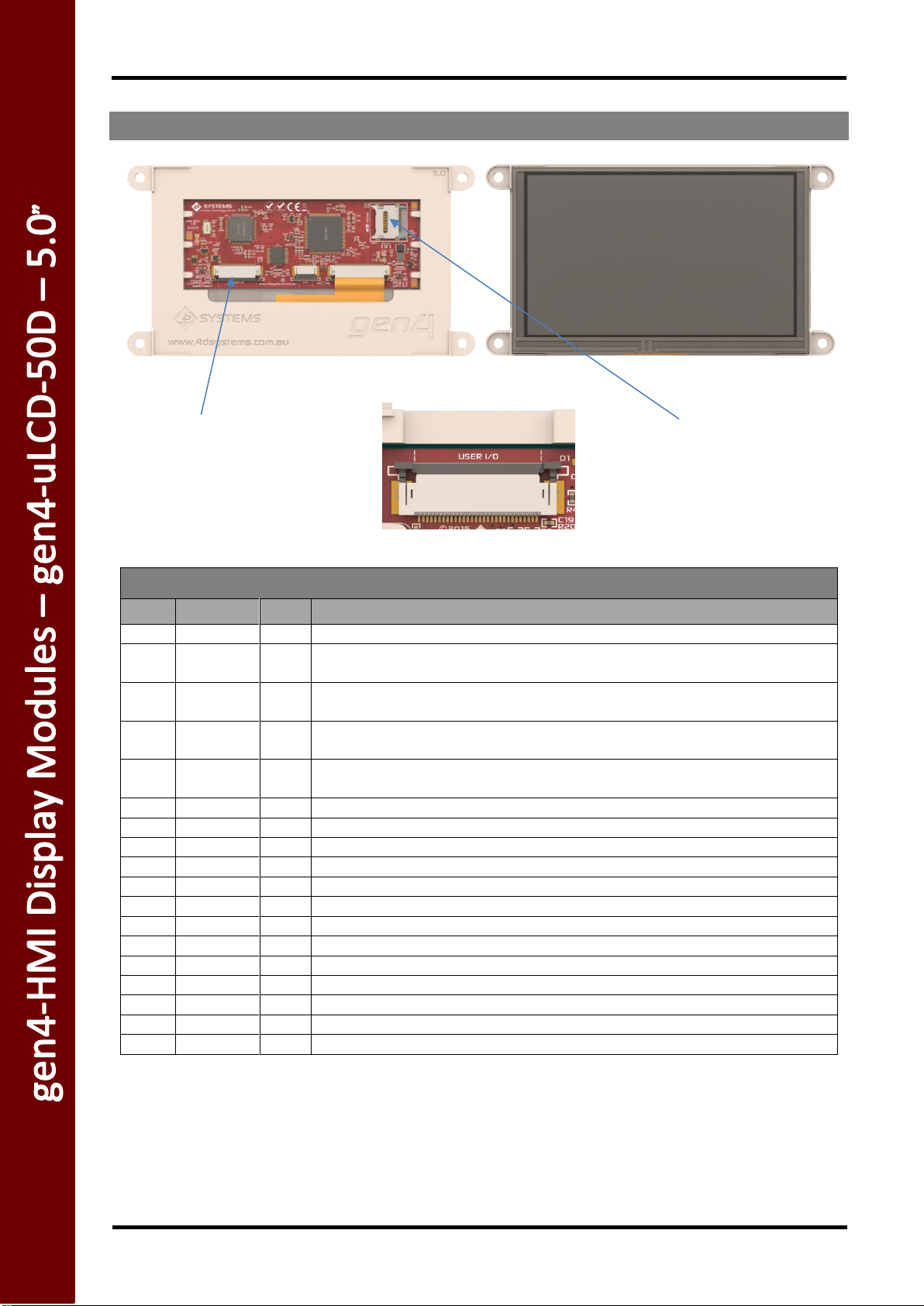
USER I/O – 30 Way FPC
Pin
Symbol
I/O
Description
1
GND
P
Supply Ground
2
PA3
I/O/A
General Purpose I/O pin with Analog Capability. This pin has a range of 0-3.3V
when used as an Analog Input, and is 3.3V tolerant only. Also used for Bus Read
3
PA2
I/O/A
General Purpose I/O pin with Analog Capability. This pin has a range of 0-3.3V
when used as an Analog Input, and is 3.3V tolerant only. Also used for Bus Write
4
PA1
I/O/A
General Purpose I/O pin with Analog Capability. This pin has a range of 0-3.3V
when used as an Analog Input, and is 3.3V tolerant only.
5
PA0
I/O/A
General Purpose I/O pin with Analog Capability. This pin has a range of 0-3.3V
when used as an Analog Input, and is 3.3V tolerant only.
6
PA9
I/O
General Purpose Input/Output, 3.3V Level - 5V Tolerant
7
PA8
I/O
General Purpose Input/Output, 3.3V Level - 5V Tolerant
8
PA7
I/O
General Purpose Input/Output, 3.3V Level - 5V Tolerant
9
PA6
I/O
General Purpose Input/Output, 3.3V Level - 5V Tolerant
10
PA5
I/O
General Purpose Input/Output, 3.3V Level - 5V Tolerant
11
PA4
I/O
General Purpose Input/Output, 3.3V Level - 5V Tolerant
12
PA10
I/O
General Purpose Input/Output, 3.3V Level - 5V Tolerant
13
PA11
I/O
General Purpose Input/Output, 3.3V Level - 5V Tolerant
14
PA12
I/O
General Purpose Input/Output, 3.3V Level - 5V Tolerant
15
PA13
I/O
General Purpose Input/Output, 3.3V Level - 5V Tolerant
16
PA14
I/O
General Purpose Input/Output, 3.3V Tolerant only. Special I2C Pin.
17
PA15
I/O
General Purpose Input/Output, 3.3V Tolerant only. Special I2C Pin.
18
NC
-
Not Connected
PIN 1
PIN 30
USER I/O – 30 way ZIF Socket
0.5mm pitch Upper Contact
15.5mm wide FPC Cable
Latch Type microSD Socket
3. Hardware Overview
gen4-HMI Display Modules
gen4-uLCD-50D Page 5 of 29 www.4dsystems.com.au
Continued overleaf…
Page 6
gen4-HMI Display Modules
USER I/O – 30 Way FPC (continued)
Pin
Symbol
I/O
Description
19
AUDIO_OUT
O
Audio Output, Filtered PWM, to feed into external amplifier
20
AUDENB
O
Audio Amplifier Enable, to enable/disable external amplifier
21
GND
P
Supply Ground
22
RESET
I
Master Reset signal. Internally pulled up to 3.3V via a 10K resistor. An active
Low pulse greater than 2 micro-seconds will reset the module. If the module
needs to be reset externally, only use open collector type circuits. This pin is
not driven low by any internal conditions. The host should control this pin via
one of its port pins using an open collector/drain arrangement.
23
RX0
I
Asynchronous Serial Receive pin, TTL level. Connect this pin to the Transmit
(Tx) signal of other serial devices. Used in conjunction with the TX pin for
programming this microLCD. This pin is tolerant up to 5.0V levels.
24
TX0
O
Asynchronous Serial Transmit pin, TTL level. Connect this pin to the Receive
(Rx) signal of other serial devices. Used in conjunction with the RX pin for
programming this microLCD. This pin is tolerant up to 5.0V levels.
25
GND
P
Supply Ground
26
5V IN
P
Main Voltage Supply +ve input pin. Reverse polarity protected. Range is 4.0V
to 5.5V, nominal 5.0V.
27
5V IN
P
Main Voltage Supply +ve input pin. Reverse polarity protected. Range is 4.0V
to 5.5V, nominal 5.0V.
28
NC
-
Not Connected
29
NC
-
Not Connected
30
GND
P
Supply Ground
I = Input, O = Output, P = Power
gen4-uLCD-50D Page 6 of 29 www.4dsystems.com.au
Page 7
gen4-HMI Display Modules
4. Hardware Interface - Pins
This section describes in detail the hardware interface
pins of the device.
4.1. Serial Ports – TTL Level Serial
The DIABLO16 Processor has three hardware
asynchronous serial ports (COM1 – COM3) that can be
configured on a variety of the processors GPIO pins.
TX/RX0 (COM0) is dedicated and its pins are fixed. All
of the DIABLO16’s serial ports can be used to
communicate with external serial devices.
TX/RX0 are referred to as COM0, and is the only one
used for programming the DIABLO16 itself.
The primary features are:
Full-Duplex 8 bit data transmission and
reception.
Data format: 8 bits, No Parity, 1 Stop bit.
Independent Baud rates from 300 baud up to
600K baud.
Single byte transmits and receives or a fully
buffered service. The buffered service feature
runs in the background capturing and
buffering serial data without the user
application having to constantly poll any of
the serial ports. This frees up the application
to service other tasks.
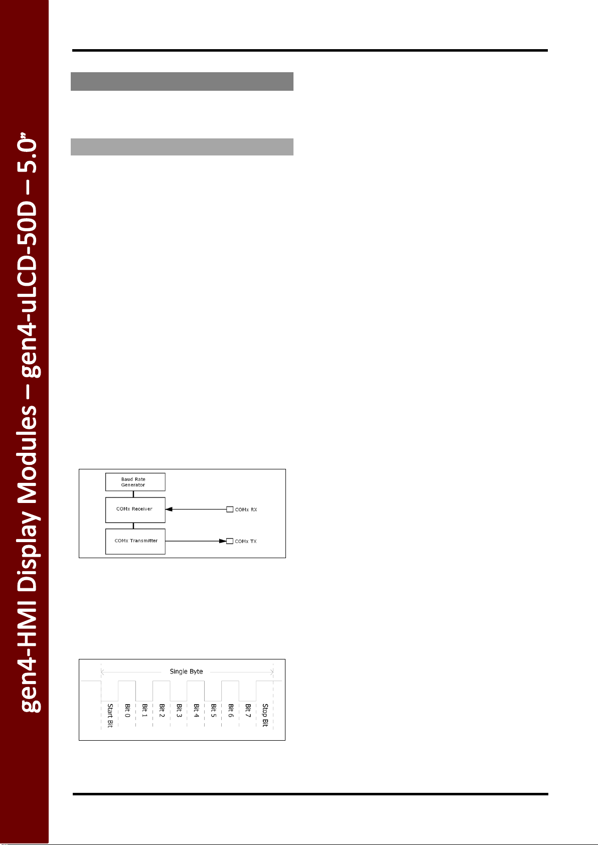
A single byte serial transmission consists of the start
bit, 8-bits of data followed by the stop bit. The start bit
is always 0, while a stop bit is always 1. The LSB (Least
Significant Bit, Bit 0) is sent out first following the start
bit. Figure below shows a single byte transmission
timing diagram.
COM0 is also the primary interface for User program
downloads, and configuration PmmC /Driver
programming. Once the compiled 4DGL application
program (EVE byte-code) is downloaded and the user
code starts executing, the serial port is then available
to the user application.
TX0 pin (Serial Transmit COM0):
Dedicated Asynchronous Serial port COM0 transmit
pin, TX0. Connect this pin to external serial device
receive (Rx) signal. This pin is 5.0V tolerant.
RX0 pin (Serial Receive COM0):
Dedicated Asynchronous Serial port COM0 receive pin,
RX0. Connect this pin to external serial device transmit
(Tx) signal. This pin is 5.0V tolerant.
TX1 pin (Serial Transmit COM1):
Asynchronous Serial port COM1 transmit pin, TX1.
Connect this pin to external serial device receive (Rx)
signal. This pin is 5.0V tolerant. This can be configured
to 1 of the GPIO pins, see table following.
RX1 pin (Serial Receive COM1):
Asynchronous Serial port COM1 receive pin, RX1.
Connect this pin to external serial device transmit (Tx)
signal. This pin is 5.0V tolerant. This can be configured
to 1 of the GPIO pins, see table following.
TX2 pin (Serial Transmit COM2):
Asynchronous Serial port COM2 transmit pin, TX2.
Connect this pin to external serial device receive (Rx)
signal. This pin is 5.0V tolerant. This can be configured
to 1 of the GPIO pins, see table following.
RX2 pin (Serial Receive COM2):
Asynchronous Serial port COM2 receive pin, RX2.
Connect this pin to external serial device transmit (Tx)
signal. This pin is 5.0V tolerant. This can be configured
to 1 of the GPIO pins, see table following.
TX3 pin (Serial Transmit COM3):
Asynchronous Serial port COM3 transmit pin, TX3.
Connect this pin to external serial device receive (Rx)
signal. This pin is 5.0V tolerant. This can be configured
to 1 of the GPIO pins, see table following.
RX3 pin (Serial Receive COM3):
Asynchronous Serial port COM3 receive pin, RX3.
Connect this pin to external serial device transmit (Tx)
signal. This pin is 5.0V tolerant. This can be configured
to 1 of the GPIO pins, see table following.
gen4-uLCD-50D Page 7 of 29 www.4dsystems.com.au
Page 8
gen4-HMI Display Modules
DIABLO16 Serial TTL Comm Port
Configuration Options
TX1
RX1
TX2
RX2
TX3
RX3
PA0
✓ ✓ ✓
PA1
✓✓ ✓✓ ✓✓
PA2
✓ ✓
✓
PA3
✓ ✓ ✓ ✓ ✓
✓
PA4
✓ ✓ ✓ ✓ ✓
✓
PA5
✓ ✓ ✓ ✓ ✓
✓
PA6
✓ ✓ ✓ ✓ ✓
✓
PA7
✓ ✓ ✓ ✓ ✓
✓
PA8
✓ ✓ ✓ ✓ ✓
✓
PA9
✓ ✓ ✓ ✓ ✓
✓
PA10
✓ ✓ ✓ PA11
✓ ✓
✓
PA12
✓ ✓ ✓ ✓ ✓
✓
PA13
✓ ✓ ✓ ✓ ✓
✓
PA14
PA15
DIABLO16 Alternate Pin Configurations
General Purpose I/O
Digital Input Digital Output Bus Read Bus Write Analog Read
PA0
✓ ✓ ✓ ✓ ✓
PA1
✓ ✓ ✓ ✓ ✓
PA2
✓ ✓ ✓ ✓ ✓
PA3
✓ ✓ ✓ ✓ ✓
PA4
✓ ✓ ✓ ✓
PA5
✓ ✓ ✓ ✓
PA6
✓ ✓ ✓ ✓
PA7
✓ ✓ ✓ ✓
PA8
✓ ✓ ✓ ✓
PA9
✓ ✓ ✓ ✓
PA10
✓ ✓ ✓
✓
PA11
✓ ✓ ✓
✓
PA12
✓ ✓ ✓ ✓
PA13
✓ ✓ ✓ ✓
PA14
✓ ✓
✓
PA15
✓ ✓
✓
4.2. General Purpose I/O
There are 16 general purpose Input/Output (GPIO)
pins available to the user. These provide flexibility of
individual bit operations along with serving
collectively for byte wise operations using the BUS
functions
Please refer to the 'DIABLO16-4DGL-Internal-
Functions.pdf' document for information on how to
set the DIABLO16 pin mappings.
As per the table, not all GPIO can be configured to be
every serial port, or RX/TX.
Serial ports output at the level of TTL 3.3V, however
are 5V tolerant, so can accept communications from
5V devices.
Please refer to the separate document titled
'DIABLO16-4DGL-Internal-Functions.pdf' for more
information.
PA0-PA3:
General purpose I/O pins, or can serve as Analog Input
pins. Each pin can be individually set for INPUT or
OUTPUT or ANALOG. Power-Up Reset default is all
INPUTS. Digital GPIO can source/sink 10mA. For more
information, the Specifications section.
These pins have a 0 to 3.3V range, and have 12 bit
resolution.
For more information, see Section 4.11 ‘Analog
Inputs’.
PA4-PA11:
General purpose I/O pins. Each pin can be individually
set for INPUT or OUTPUT. Power-Up Reset default is
all INPUTS. When set as Digital Inputs, the pins are 5V
tolerant. Digital GPIO can source/sink 10mA. For more
information, see the Specifications Section.
gen4-uLCD-50D Page 8 of 29 www.4dsystems.com.au
Page 9
gen4-HMI Display Modules
DIABLO16 Alternate Pin Configurations
I/O Support Functions
Pulse Out PWM Out Pin Counter Quadrature In
PA0 ✓
✓ PA1
✓
✓ PA2 ✓
✓ PA3 ✓
✓ PA4
✓ ✓ ✓
✓
PA5
✓ ✓ ✓
✓
PA6
✓ ✓ ✓
✓
PA7
✓ ✓ ✓
✓
PA8
✓ ✓ ✓
✓
PA9
✓ ✓ ✓
✓
PA10
✓
PA11
✓
PA12
✓ PA13
✓
PA14
PA15
PA12-PA13:
PA12 and PA13 are reserved for the capacitive touch
controller on the DCT-CLB model. These pins should
not be connected else Touch performance may be
degraded. There are 4.7K pullup resistors on each of
these GPIO. Avoid these pins in normal situations on
this DCT-CLB model. Using these pins on non-touch
(D/D-CLB) and resistive touch (DT) modules is however
OK, or in situations where touch is not required. These
pins are 5V tolerant.
PA14-PA15:
General purpose I/O pins. Each pin can be individually
set for INPUT or OUTPUT. Power-Up Reset default is
all INPUTS. When set as Digital Inputs, the pins are
3.3V tolerant. Digital GPIO can source/sink 10mA.
Under special situations, these pins can be utilised for
a high speed I2C interface. Please refer to table in
section 4.4 and information in section 4.6.
Note: Digital GPIO pins are 5.0V tolerant, except PA14PA15, which are 3.3V tolerant only. PA0-PA3 are 3.3V
tolerant only. All pins output at 3.3V levels.
4.4. Alternate Pin Function Overview
Most of the GPIO pins have an alternate function other
than being for General Purpose I/O.
GPIO pins can be configured to be SPI, I2C, Serial or a
range of other functions.
Note: Not all pins can be configured to be any of the
alternate pin functions. Please refer to the tables.
Please refer to the following tables which illustrate
which pins can be associated alternative functions.
4.3. System Pins
+5V IN (Module Voltage Input)
Module supply voltage input pins. Both of these pins
should be connected to a stable supply voltage in the
range of 4.0 Volts to 5.5 Volts DC. Nominal operating
voltage is 5.0 Volts. Note backlight brightness will be
lower for voltages under 5.0V.
GND (Module Ground)
Device ground pins. At least two pins should be
connected to ground.
RESET (Module Master Reset)
Module Master Reset pin. An active low pulse of
greater than 2μs will reset the module. Internally
pulled up to 3.3V via a 10K resistor. Only use open
collector type circuits to reset the device if an external
reset is required.
AUDENB (Audio Enable Output)
Output dedicated to enable or disable and external
amplifier, where required.
AUDIO (PWM Audio Output)
Output specifically for Audio. This pin is a PWM output
from the DIABLO16 Processor. This pin is a 3.3V level
PWM output to drive an external amplifier with
DIABLO16 generated Audio, via an external filtering
circuit to turn digital PWM into Analog. Note that
AUDENB must be enabled in DIABLO16 for any input
signal to be heard.
The previous table illustrates which of the GPIO can be
used for the four different I/O Support Functions.
Note: Once a pin is allocated to an alternate function,
another pin cannot also be allocated to the same
alternate function.
Please refer to the separate document titled
'DIABLO16-4DGL-Internal-Functions.pdf' for more
information on how to set the alternate pin
configurations.
The Alternate pin functions have been broken up into
a few tables for simplification. There are
communication based functions, and I/O support
based functions.
gen4-uLCD-50D Page 9 of 29 www.4dsystems.com.au
Page 10

DIABLO16 Alternate Pin Configurations
SPI Communications
SPI1 SDO SPI1 SDI SPI1 SCK SPI2 SDO SPI2 SDI SPI2 SCK SPI3 SDO SPI3 SDI SPI3 SCK
PA0
✓ ✓ ✓
PA1
✓✓ ✓✓✓ ✓✓✓ ✓
PA2
✓
✓
✓
PA3
✓ ✓ ✓ ✓ ✓ ✓ ✓ ✓ ✓
PA4
✓ ✓ ✓ ✓ ✓ ✓ ✓ ✓ ✓
PA5
✓ ✓ ✓ ✓ ✓ ✓ ✓ ✓ ✓
PA6
✓ ✓ ✓ ✓ ✓ ✓ ✓ ✓ ✓
PA7
✓ ✓ ✓ ✓ ✓ ✓ ✓ ✓ ✓
PA8
✓ ✓ ✓ ✓ ✓ ✓ ✓ ✓ ✓
PA9
✓ ✓ ✓ ✓ ✓ ✓ ✓ ✓ ✓
PA10
✓
✓
✓
PA11
✓ ✓ ✓
PA12
✓ ✓ ✓ ✓ ✓ ✓ ✓ ✓ ✓
PA13
✓ ✓ ✓ ✓ ✓ ✓ ✓ ✓ ✓
PA14
PA15
DIABLO16 Alternate Pin Configurations
I2C Communications
I
2
C1 SDA
I
2
C1 SCL
I
2
C2 SDA
I
2
C2 SCL
I
2
C3 SDA
I
2
C3 SCL
PA0
✓ ✓ ✓ ✓ ✓
✓
PA1
✓ ✓ ✓ ✓ ✓ ✓ PA2
✓ ✓ ✓ ✓ ✓
✓
PA3
✓ ✓ ✓ ✓ ✓
✓
PA4
✓ ✓ ✓ ✓ ✓ ✓ PA5
✓ ✓ ✓ ✓ ✓
✓
PA6
✓ ✓ ✓ ✓ ✓
✓
PA7
✓ ✓ ✓ ✓ ✓
✓
PA8
✓ ✓ ✓ ✓ ✓
✓
PA9
✓ ✓ ✓ ✓ ✓
✓
PA10
✓ ✓ ✓ ✓ ✓
✓
PA11
✓ ✓ ✓ ✓ ✓
✓
PA12
✓ ✓ ✓ ✓ ✓
✓
PA13
✓ ✓ ✓ ✓ ✓
✓
PA14
SPECIAL SPECIAL SPECIAL
PA15
SPECIAL SPECIAL SPECIAL
Further information is available in the next sections for
each of the alternative pin functions.
Note: Quadrature In requires 2 Pins
The following table illustrates which of the GPIO can
be used for the three different SPI channels available.
The following table illustrates which of the GPIO can
be used for the three different I2C channels available.
gen4-HMI Display Modules
SPECIAL – please see Section 4.6
4.5. SPI
There are 3 user configurable SPI channels available
for mapping to GPIO, for use by the user for the target
application. All 3 SPI channels are Master only, and
cannot be configured to be slaves at this time.
The SPI Bus speed is configurable using the SPIx_Init()
Function in 4DGL, and allows various speeds from
78.125Khz to 17.5Mhz.
Please refer to the table on the previous page for
details on which GPIO can be configured for SPI.
Note: The additional SPI channel (SPI0) is dedicated to
memory cards and cannot be reconfigured for
alternate uses.
To map an SPI channel to a set of GPIO pins, the
following 4DGL functions are used:
SPIx_SCK_pin(pin); // Map the SCK pin
SPIx_SDI_pin(pin); // Map the SDI pin
SPIx_SDO_pin(pin); // Map the SDO pin
Where ‘SPIx’ is substituted with SPI1, SPI2 or SPI3
accordingly, and ‘pin’ is the target GPIO pin compatible
with that particular pin function.
Chip Select for use with SPI can be any other unused
GPIO pin, configured as a Digital Output. The lowering
and raising of the selected CS (GPIO) pin is done
manually by the user is the 4DGL application.
Please refer to the separate document titled
'DIABLO16-4DGL-Internal-Functions.pdf' for more
information on how to use the SPI functions, along
with the separate document titled ‘DIABLO16-
Processor-Datasheet-REVx.x.pdf’.
gen4-uLCD-50D Page 10 of 29 www.4dsystems.com.au
4.6. I2C
There are 3 user configurable I2C channels available for
mapping to GPIO, for use by the user for the target
application. All 3 I2C channels are Master only, and
cannot be configured to be slaves at this time.
Please refer to the table on the previous page for
details on which GPIO can be configured for I2C.
To map an I2C Channel to a set of GPIO pins, the
following 4DGL function is used:
I2Cx_Open(Speed, SCLpin, SDApin);
Page 11

gen4-HMI Display Modules
Where ‘I2Cx’ is substituted with I2C1, I2C2 or I2C3
accordingly, ‘Speed’ is the desired I2C Bus speed, and
‘SCLpin’ and ‘SDApin’ are the target GPIO pins
compatible with that particular pin function.
Note: The normal I2C pins are PA0 to PA13, however
use of these pins has a few limitations.
a) There is no slew rate control at I2C_MED
b) I2C_FAST is not truly 1MHz.
If either of these restrictions need to be addressed, a
special case of SCLpin = PA14 and SDApin = PA15 exists
ONLY for speeds I2C_MED (which uses slew rate
control) and I2C_FAST (which is truly 1MHz)
Please refer to the separate document titled
'DIABLO16-4DGL-Internal-Functions.pdf' for more
information on how to use the I2C functions, along
with the separate document titled ‘DIABLO16-
Processor-Datasheet-REVx.x.pdf’.
4.7. Pulse Out
Pulse Out is used to create a single pulse of set
duration on the selected pin of choice, which is
inverted in polarity to the current state of the pin.
This ‘inversion of polarity’ means if a Pin is currently
held HI, and Pulse Out is executed on that Pin, the pin
will pulse LO and then return to HI. Same with vice
versa, if currently LO and Pulse Out is executed on that
Pin, it will pulse HI and then return to LO.
This is available in both blocking and non-blocking
versions.
Please refer to the table on the previous page for
details on which GPIO can be configured to this.
Note: Each Pulse Out request needs at least a 1ms
lead time due to the scheduling of the event with the
internal 1ms timer.
To enable the Pulse Out function on a GPIO pin, the
following 4DGL functions are used:
pin_Pulseout(pin, value); //Non-Blocking
pin_PulseoutB(pin, value); //Blocking
Where ‘pin’ is the target GPIO pin compatible with that
particular pin function, and ‘value’ is the length of the
pulse in milliseconds.
Please refer to the separate document titled
'DIABLO16-4DGL-Internal-Functions.pdf' for more
information on how to use the Pulse Out functions,
along with the separate document titled ‘DIABLO16-
Processor-Datasheet-REVx.x.pdf’.
4.8. PWM Out
There are 6 PWM channels available to be configured
by the user, with 4 time bases available for selection.
The PWM can be configured to be used in Servo Mode,
or Simple Mode.
Please refer to the table on the previous page for
details on which GPIO can be configured for PWM.
Servo Mode allows a millisecond input value with
0.01ms resolution, which runs at a frequency of
approximately 50Hz or 50pps (20ms). The position of
the servo is determined by the width of the pulse.
Generally 1.5ms is 90 degrees, 1ms being 0 degrees
and 2ms being 180 degrees. Servos however vary, and
the DIABLO16 PWM control can be adjusted to suit
most applications.
Simple Mode allows a percentage input value with
resolution of 0.1%, which runs at a frequency of
approximately 70KHz.
To enable the PWM output on a GPIO pin, the
following 4DGL function is used:
PWM_Init(pin, mode, value);
Where ‘pin’ is the GPIO compatible with the particular
pin function, ‘mode’ is the type of PWM to generate,
and ‘value’ is the parameter which defined the PWM
pulse itself.
Please refer to the separate document titled
'DIABLO16-4DGL-Internal-Functions.pdf' for more
information on how to use the SPI functions, along
with the separate document titled ‘DIABLO16-
Processor-Datasheet-REVx.x.pdf’.
4.9. Pin Counter
There are 6 Pin Counter channels available to be
configured by the user, used to count incoming pulses
with the ability to call a user function on overflow. The
Pin Counter function is available for use in a variety of
modes.
The counters can be read and written at any time.
Please refer to the table in section 4.4 ‘Alternate Pin
Functions – Overview’ for details on which GPIO can
be configured for this.
To enable the Pin Counter function on a GPIO pin, the
following 4DGL function is used:
pin_Counter(pin, mode, OVFfunction);
gen4-uLCD-50D Page 11 of 29 www.4dsystems.com.au
Page 12

gen4-HMI Display Modules
Where ‘pin’ is the GPIO pin compatible with this
particular function, ‘mode’ is the type of trigger used
to count on such as Rising/Falling/Edge, and
‘OVFfunction’ is the user function to call when the
counter overflows, if desired.
Please refer to the separate document titled
'DIABLO16-4DGL-Internal-Functions.pdf' for more
information on how to use the Pin Counter functions,
along with the separate document titled ‘DIABLO16-
Processor-Datasheet-REVx.x.pdf’.
4.10. Quadrature In
There are two Quadrature Input channels available on
the DIABLO16 processor, which requires 2 GPIO pins
each.
Please refer to the table on the previous page for
details on which GPIO can be configured for
Quadrature Input.
Quadrature Input allows a quadrature encoder to be
connected, and the position counter and delta counter
can be read at any time.
To enable the Quadrature Input function on a set of
GPIO pins (2 pins required), the following 4DGL
function is used:
Qencoderx(PHApin, PHBpin, mode);
Where ‘Qencoderx’ is substituted for Quencoder1 or
Quencoder2 accordingly, ‘PHApin’ is the pin
connected to the A Phase of the Encoder, ‘PHBpin’ is
the pin connected to the B Phase of the Encoder, and
‘mode’ is not currently used so is to be set to zero (0).
Please refer to the separate document titled
'DIABLO16-4DGL-Internal-Functions.pdf' for more
information on how to use the Quadrature Input
functions, along with the separate document titled
‘DIABLO16-Processor-Datasheet-REVx.x.pdf’.
4.11. Analog Inputs
Please refer to the table in section 4.2 for details on
which GPIO can be configured to be analog inputs.
The analog inputs on the DIABLO16 have a range of 0
to 3.3V, each with a max resolution of 12-bits.
The analog inputs can be read using three modes,
standard mode, averaged mode or high speed mode.
Standard Mode results in a sample being immediately
read. Standard Mode can read over 40000 values per
second. Operates at 12-bit.
Averaged Mode results in a 16 sample being
immediately read and their average returned.
Averaged Mode can read approximately 20000 values
per second. Operates at 12-bit.
Highspeed Mode collects a user specified number of
samples at a user specified rate/frequency and can
execute a user function when complete. The updated
value updates approximately 250000 times across 1-4
channels. Operates at 10-bit.
To enable a GPIO to be used as an Analog Input for
Standard or Averaged modes, the following 4DGL
function is used to set the pin:
pin_Set(mode, pin);
Where ‘mode’ is the desired mode defined above,
either Standard or Averaged, and ‘pin’ is the GPIO
compatible with this function which is to become an
Analog Input.
For highspeed mode, the following 4DGL function is
used to set the pin and define the parameters:
ana_HS(rate, samples, 1buf, 2buf, 3buf, 4buf, func);
Where ‘rate’ is the number of samples per second,
‘samples’ is the number of samples to collect per
channel, ‘1buf’ ‘4buf’ are the buffer addresses for
the 4 channels, and ‘func’ is the user function to call
when the number of samples specified have been
collected.
Please refer to the separate document titled
'DIABLO16-4DGL-Internal-Functions.pdf' for more
information on the Analog Input functions, along with
the separate document titled ‘DIABLO16- Processor-
Datasheet-REVx.x.pdf’.
Note: Analog Inputs are 0-3.3V tolerant only. Do not
apply voltages outside of this range as you will
damage Diablo16.
gen4-uLCD-50D Page 12 of 29 www.4dsystems.com.au
Page 13

gen4-HMI Display Modules
5. Module Features
The gen4 series of Integrated Display Modules are
designed to accommodate most applications. Some of
the main features of the module are listed below.
5.1. DIABLO16 Processor
The module is designed around the DIABLO16
Graphics Controller from 4D-Labs.
The DIABLO16 is a smart Controller and the interface
to the TFT- LCD displays is almost plug-n-play.
All of the data and control signals are provided by the
chip to interface directly to the display.
Powerful graphics, text, image, animation and
countless more features are built right inside the chip.
The data sheet for the processor is available from the
http://www.4dsystems.com.au website:
“DIABLO16 Processor Datasheet”
5.2. Audio
Audio playback support in the DIABLO16 Processor
enables this module to play audio WAV files stored in
the micro-SD memory card. Filtered PWM audio is
generated and made available on the AUDIO pin of the
30 way ZIF connector, ready to interface with an audio
amplifier on your application board.
A simple instruction enables the user to
play/pause/stop audio files while continuing the
execution of the user application code, such as display
updates, touch recognition, communications, etc. The
audio system also allows real time pitch change of
audio samples.
For a complete list of audio commands please refer to
the separate document titled:
“DIABLO16 4DGL Internal Functions”
5.3. SD/SDHC Memory Cards
The module supports micro-SD memory cards via the
on-board latch type micro-SD connector. The memory
card is used for all multimedia file
retrieval such as images, animations
and movie clips. The memory card
can also be used as general purpose
storage for data logging applications. Support is
available for off-the-shelf micro-SD (< 4GB) and high
capacity HC memory cards (4GB and above). Memory
cards up to 32GB is size can be used, however it must
be noted that only a portion of this can be utilised by
the FAT16 file system. See section below for more
details.
Note: A microSD card capable of SPI is a requirement
for all 4D Systems’ display modules powered by
Goldelox, Picaso or Diablo16 Processors. If a non-SPI
compatible card is used, it will simply fail to mount, or
may cause intermittent issues resulting in lock ups and
crashing of the application. Please refer to the 4D
Systems website for microSD cards offered by 4D
Systems.
5.4. FAT16
All 4D Systems display modules featuring 4D Labs
processors use off-the-shelf standard SDHC/SD/microSD memory cards (SPI Compatible Only) with up to
4GB capacity usable with FAT16 formatting.
For any FAT file related operations, before the
memory card can be used it must first be formatted
correctly. Built into Workshop4 is a tool created by 4D,
called RMPET (please refer to the Tools menu, in any
Environment, inside the Workshop4 IDE). RMPET
allows the User to easily partition and format microSD
cards, to make their file system ready to be used with
4D Systems modules. The formatting of the card can
be done on any PC system with a card reader.
The DIABLO16 Processor also supports high capacity
HC memory cards (4GB and above). The available
capacity of SD-HC cards varies according to the way
the card is partitioned and the commands used to
access it. Refer to the 4D Systems RMPET tool in the
Workshop4 IDE.
A Max of 4GB can be utilised by the FAT16 file system.
The FAT partition is always first (if it exists). Any space
larger than 4GB will be RAW, and can still be utilised
by your 4D Systems module, using different functions.
Please refer to Application Notes.
gen4-uLCD-50D Page 13 of 29 www.4dsystems.com.au
Page 14

gen4-HMI Display Modules
5.5. Application PCB Support
The gen4 5.0” Diablo16 Integrated Display Module is
designed to accommodate a range of applications, and
therefore is suited for those wanting to make a
customised module, without the need for piggy-back
or daughter boards mounted on headers.
On the back of the gen4 module, the display related
circuitry will be found, which is recessed into the
plastic. The level of the plastic on the back of the gen4
module is higher than the tallest component on the
display circuit PCB, meaning an Application PCB can be
mounted on the back of the gen4, without affecting
the display related circuitry.
The image below (4.3” model depicted) shows a mock
Application PCB on the back of the gen4 display (Blue
area). It features a cut-out in the PCB so access to the
micro-SD socket on the gen4’s display board is
possible, however this may or may not be required
depending on the application and if the micro-SD
socket is utilised or requiring access once the
Application PCB is applied.
5.6. RF / EMI Shielding Support
As per what is written in section 5.5 (Application PCB
Support), there is an option for extended RF shielding
and EMI protection on this module.
On the back of the gen4’s display PCB, are grounded
plated ‘X pads’, which make contact with the metal
housing of the display.
Where the Application PCB is shown to sit in Section
5.5, can house a small metal shield of the same size.
This shield is used instead of, or underneath an
Application PCB, to aid the on-board electronics in the
prevention from potential RF or EMI signals.
On the top of the display PCB is more GND pads, which
can have a pogo pin or similar device mounted on
them, which can make contact with this metal shield.
The display electronics are then sandwiched between
the display’s metal housing, and the metal shield, all
connected together with a common ground.
NOTE: There are no guarantees these steps will
increase chances or grant access to EMI related
The 30 way FFC flex cable out of the gen4 into the
application board can either turn up through a slot in
the application board, or can travel down under the
gen4 plastic and emerge at the bottom, and then into
the application board (as depicted above).
The micro-SD socket is a latch type, so it is accessible
from the top, rather than a push/push or push/pull
style which is accessible from the side.
certifications, however the gen4 has the capability to
utilise shielding of the modules electronics, should the
need arise. This may or may not assist the User with
protecting the device against EMI/EMF/RF type noise,
depending on the source, strength and type of noise
present, however should aid in the protection.
gen4-uLCD-50D Page 14 of 29 www.4dsystems.com.au
Page 15

gen4-HMI Display Modules
6. Display/Module Precautions
Avoid having to display the same image/object on
the screen for lengthy periods of time. This can
cause a burn-in which is a common problem with
all types of display technologies. Blank the screen
after a while or dim it very low by adjusting the
contrast. Better still; implement a screen saver
feature.
Moisture and water can damage the display.
Moisture on the surface of a powered display
should not cause any problems, however if water
is to enter the display either from the front or
from the rear, or come in contact with the PCB,
damage will certainly occur. Wipe off any
moisture gently or let the display dry before
usage. If using this display module in an
environment where it can get wet, ensure an
appropriate enclosure is used.
Dirt from fingerprint oil and fat can easily stain the
surface of the display. Gently wipe off any stains
with a soft lint-free cloth.
The performance of the display will degrade
under high temperature and humidity. Avoid such
conditions when storing.
Do not tamper with the display flex cable that is
connected to the control board. This may affect
the connection between the display and the
driving circuitry and cause failure.
Displays are susceptible to mechanical shock and
any force exerted on the module may result in
deformed zebra stripes, a cracked display cell and
broken backlight
Always use the mounting holes on the module's
corner plates to mount the display where
possible.
Display modules have a finite life, which is
typically dictated by the display itself, more
specifically the backlight. The backlight contains
LED’s, which fade over time. In the Specifications
section is a figure for the typical life of the display,
and the criteria are listed.
Resistive Touch model features a touch sensitive
film over the display which is sensitive to
pressure. Take note when mounting the display
module in an enclosure that pressure is not
applied to the surface of the display by the
enclosure, or false touches will occur, or the touch
will simply not function at all.
7. Hardware Tools
The following hardware tools are required for full
control of the gen4 Integrated Display Modules.
7.1. 4D Programming Cable/Adaptor
The 4D programming interfaces are used to program a
new Firmware/PmmC, Display Driver and for
downloading compiled 4DGL code into the processor.
They even serve as an interface for communicating
serial data to the PC.
The 4D Programming Cable is a USB to Serial-TTL UART
converter cable incorporating the Silabs CP2102 USB
to Serial UART bridge IC.
4D Programming Cable
Please note, in conjunction with a Programming Cable
or a Programming Adaptor, the gen4 series of Display
Modules requires a simple interface board (gen4-IB),
as there is no 5 way male header on gen4 modules like
other 4D Systems modules.
The gen4 Interface boards (gen4-IB) ship with each
gen4 Display Module unless otherwise stated. Simply
connect the supplied 30 way FPC cable into the ZIF
connector on the gen4 Interface Board, and connect
the Programming Cable or Adaptor into the 5-way
header on the Interface Board. You are now ready to
program using a 4D Programming Cable. This can also
be used to interface to other devices such as a 4D
Arduino Adaptor Shield, breadboard etc.
gen4-uLCD-50D Page 15 of 29 www.4dsystems.com.au
Page 16

gen4-HMI Display Modules
An alternative to using a gen4-IB and a 4D
Programming Cable, is a single all in one board called
the 4D-UPA (4D Universal Programming Adaptor).
4D-UPA
The 4D-UPA minimizes the connections and modules
required for programming—creating a single module
with microUSB interface, and DIP style pads for GPIO
breakout of all the signals used on the gen4 Display
interface, which is useful for development or final
product use.
Note: In addition to these modules, the gen4-PA and
uUSB-PA5/uUSB PA5-II can still be used. Please be
reminded though that these still need a gen4-IB in
order to be used for programming.
Either the 4D Programming Cable or 4D-UPA
Programming Adaptor can be used for the gen4 series
of Display Modules. Using a non-4D programming
interface could damage your processor, and void your
Warranty.
These programming interfaces are available from 4D
Systems, www.4dsystems.com.au.
8. Software Overview - Language
The DIABLO16 processor belongs to a family of
processors powered by a highly optimised soft core
virtual engine called EVE (Extensible Virtual Engine).
EVE was designed and created by 4D Systems in the
early 2000’s, and should not be confused by FTDI’s
solution of EVE, which was developed a decent decade
or so later.
EVE is a proprietary, high performance virtualmachine with an extensive byte-code instruction set
optimised to execute compiled 4DGL programs.
4DGL (4D Graphics Language) was specifically
developed from ground up for the EVE engine core. It
is a high level language which is easy to learn and
simple to understand yet powerful enough to tackle
many embedded graphics applications.
4DGL is a graphics oriented language allowing rapid
application development, and the syntax structure
was designed using elements of popular languages
such as C, Basic, Pascal and others.
Programmers familiar with these languages will feel
right at home with 4DGL. It includes many familiar
instructions such as IF..ELSE..ENDIF, WHILE..WEND,
REPEAT..UNTIL, GOSUB..ENDSUB, GOTO, PRINT as
well as some specialised instructions SERIN, SEROUT,
GFX_LINE, GFX_CIRCLE and many more.
For detailed information pertaining to the 4DGL
language, please refer to the following documents:
“4DGL Programmers Reference Manual”
“DIABLO16 4DGL Internal Functions”
These are both available for download on the
Workshop4 Product Page of the 4D Systems website.
To assist with the development of 4DGL applications,
the Workshop4 IDE combines a full-featured editor, a
compiler, a linker and a downloader into a single PCbased application. It's all you need to code, test and
run your applications.
4DGL is available to be written in two of the four
environments offered by the Workshop 4 IDE,
Designer and ViSi. The other two environments, Serial
and ViSi-Genie do not directly use 4DGL by the User
(Except in Workshop4 Pro, for ViSi-Genie), however it
is present in the background. Serial is an application
which runs, and that is written in 4DGL. ViSi-Genie
automatically generates 4DGL itself based on what is
configured in the GUI. More information about each
follows.
gen4-uLCD-50D Page 16 of 29 www.4dsystems.com.au
Page 17

gen4-HMI Display Modules
9. 4D Systems - Workshop 4 IDE
Workshop 4 is a comprehensive software IDE that
provides an integrated software development
platform for all of the 4D family of processors and
modules. The IDE combines the Editor, Compiler,
Linker and Downloader to develop complete 4DGL
application code. All user application code is
developed within the Workshop 4 IDE.
The Workshop 4 IDE supports multiple development
environments for the user, to cater for different user
requirements and skill levels.
The Designer environment enables the user to
write 4DGL code in its natural form to program
the range of 4D Systems intelligent displays.
A visual programming experience, suitably called
ViSi, enables drag-and-drop type placement of
objects to assist with 4DGL code generation and
allows the user to visualise how the display will
look while being developed.
An advanced environment called ViSi-Genie
doesn’t require any 4DGL coding at all, it is all
done automatically for you. Simply lay the display
out with the objects you want, set the events to
drive them and the code is written for you
automatically. This can be extended with
additional features when a Workshop4 PRO
license is purchased from the 4D Systems website.
Extended Advanced features for Visi-Genie are
available in PRO version of WS4. Further details
explained in section 9.3.
A Serial environment is also provided to
transform the display module into a slave serial
module, allowing the user to control the display
from any host microcontroller or device with a
serial port.
The Workshop 4 IDE is available from the 4D Systems
website. www.4dsystems.com.au
For comprehensive manuals on the Workshop 4 IDE
Software, the language, and its environments, refer to
the documentation from the 4D Systems website, on
the Workshop 4 product page.
9.1. Workshop4 - Designer
Choose the Designer environment to write 4DGL code
in its raw form.
The Designer environment provides the user with a
simple yet effective programming environment where
pure 4DGL code can be written, compiled and
downloaded to the range of 4D Systems intelligent
display modules.
Designer is a very powerful environment, for those use
to developing without any form of GUI aid, or for those
developing complex systems where no aid is required.
9.2. Workshop4 – ViSi
ViSi was designed to make the creation of graphical
displays a more visual experience.
ViSi is a great software tool that allows the user to see
the instant results of their desired graphical layout.
Additionally, there is a selection of inbuilt dials, gauges
and meters that can simply be placed onto the
simulated module display. From here each object can
have its properties edited, and at the click of a button
all relevant 4DGL code associated with that object is
produced in the user program. The user can then write
4DGL code around these objects to utilise them in the
way they choose.
gen4-uLCD-50D Page 17 of 29 www.4dsystems.com.au
Page 18

gen4-HMI Display Modules
9.3. Workshop4 – ViSi Genie
ViSi-Genie is a breakthrough in the way 4D Systems’
graphic display modules are programmed. It is an
environment like no other, a code-less programming
environment that provides the user with a rapid visual
experience, enabling a simple GUI application to be
‘written’ from scratch in literally seconds.
ViSi-Genie does all the background coding, no 4DGL to
learn, it does it all for you.
Pick and choose the relevant objects to place on the
display, much like the ViSi Environment yet without
having to write a single line of code. Each object has
parameters which can be set, and configurable events
to animate and drive other objects or communicate
with external devices.
Simply place an object on the screen, position and size
it to suit, set the parameters such as colour, range,
text, and finally select the event you wish the object to
be associated with, it is that simple.
In seconds you can transform a blank display into a
fully animated GUI with moving sliders, animated
press and release buttons, and much more. All without
writing a single line of code!
ViSi-Genie provides the user with a feature rich rapid
development environment, second to none.
9.4. Workshop4 – Serial
The Serial environment in the Workshop 4 IDE
provides the user the ability to transform a 4D Systems
Intelligent Display, into a slave serial graphics
controller.
This enables the user to use their favourite
microcontroller or serial device as the Host, without
having to learn 4DGL or program in a separate IDE.
Once the display module is configured by the Serial
Environment (by downloading what is called the SPE
application to the module), commands can be sent
from the users host microcontroller to display
primitives, images, sound and video, and can even be
used to display ViSi generated graphics and widgets.
The Serial Environment should not be taken as being
basic in terms of its capabilities, as it has the full 4DGL
command set behind it, but available from the Host
rather than from programming the display module
itself using the Workshop4 IDE.
Virtually anything created in Designer or ViSi, can be
designed or controlled from the Serial Environment.
Please refer to the “Diablo16 Serial Command Set
Reference Manual” from the Workshop 4 product
page on the 4D Systems website for a complete listing
of all the supported Serial commands
ViSi-Genie’s functionality can be extended with the
purchase of a Workshop4 PRO License.
Workshop4 PRO adds a professional set of features to
the Visi-Genie environment called Genie-Magic. The
added features allow the user to add in 4DGL scripts,
which can be activated from the display itself, from an
interfacing Host, or from an external sensor or device.
These PRO set of features of Genie-Magic allow the
User to create an immensely powerful GUI system
with a fraction of the effort required by other systems.
gen4-uLCD-50D Page 18 of 29 www.4dsystems.com.au
Page 19

gen4-HMI Display Modules
9.5. PmmC/Firmware Programming
The DIABLO16 processor is a custom graphics
processor. All functionality including the high level
commands are built into the chip. This chip level
configuration is available as a PmmC (Personalitymodule-micro-Code) file, which can be likened to
traditional Firmware. There is also a Display Driver file,
which separates specific display settings from the
PmmC, unlike on the PICASO processor where
everything is combined.
A PmmC file contains all of the low level micro-code
information (analogy of that of a soft silicon) which
define the characteristics and functionality of the
device. The ability of programming the device with a
PmmC file provides an extremely flexible method of
customising as well as upgrading it with future
enhancements.
The Display Driver contains the initialisation and
parameters associated with the particular display that
is to be connected to the DIABLO16 processor, along
with product specific settings and parameters which
are required over and above what is found in the
PmmC.
The PmmC file and Display Driver file can only be
programmed into the device via the COM0 serial port
with the aid of Workshop 4, the 4D Systems IDE
software.
Solutions, which remove the need to use Workshop4
to program the display modules, are available for
commercial customers requiring batch programming
or production line programming. These solutions are
practical for production staff and minimize the chance
of unwanted or unauthorised modifications on the
production line.
Three solutions come with the Workshop4 IDE, which
can be separated out for production line computers if
required, ScriptC, PmmC Loader and Program Loader.
ScriptC is a command line interface which can be
controlled from a Batch Script or similar, useful for
repetitive loading or when controlled from an external
application. Example scripts are provided, showing
how to load PmmC, Display Drivers and Applications
using a batch script.
PmmC Loader is a GUI interface designed to download
PmmC’s and Drivers to 4D Systems Processor. It has
the ability to automatically update existing PmmC’s
and Drivers present on a module, or to manually
change or force download to a blank processor or
module, overwriting anything written in previously.
Program Loader is a GUI interface designed to
download Applications to either Flash or RAM, useful
for testing or production loading, without the need for
Workshop4 itself.
Please contact our Support Team for more
information on what we can provide. Some solutions
also exist for external processor based loading, if there
is a requirement for that. This solution is available
under NDA.
Using a non-4D programming interface could damage
your module, and void your Warranty.
gen4-uLCD-50D Page 19 of 29 www.4dsystems.com.au
Page 20

gen4-HMI Display Modules
10. Starter Kit
4D Systems highly recommends all first time buyers of
4D Systems’ displays, to purchase the Starter Kit when
purchasing their first 4D Systems display solution.
The Starter Kit provides all the hardware that is
required to get the User up and running.
Not all development environments and features will
be needed by every User. However, by purchasing the
display solution in a Starter Kit allows you to take full
advantage of all of the features of the 4D Systems
Display Solution and try out each of the 4D Woskshop4
Environments prior to settling with the preferred
feature-set.
The Designer environment can utilise every feature of
the display, however depending on the user
requirements, a micro-SD (uSD) card may not be
required. The uSD card is used when displaying
images/video/sound, along with datalogging to uSD,
and a programming cable or adaptor is required for
downloading compiled code and PmmC/Firmware
updates.
The ViSi environment is the same as Designer in terms
of feature utilisation, but is image based so requires a
uSD card, along with a programming cable.
The ViSi-Genie environment is also image based, and
therefore requires a uSD card and programming cable
also.
The Serial environment does not require either a uSD
or Programming cable to be used once the module has
been configured as a Serial device, however can utilise
both depending on the user requirements. The uSD
card can be used for such things as storage and display
of multimedia files, datalogging, and the Programming
cable for PmmC/Firmware updates, or changing to one
of the other three programming environments.
Starter Kits typically include:
gen4 Integrated Display Module
gen4 Interface Module (gen4-IB)
4D Universal Programming Adaptor (4D-UPA)
4GB micro-SD Card
5-way cable for easy connection to a
breadboard or host via the gen4-IB
150mm 30-way FFC cable for connecting
gen4 display to gen4-IB or 4D-UPA
Quick Start Guide
Please refer to the 4D Systems website for current
components included in the Starter Kit.
Simply select the Starter Kit option when purchasing
the chosen display module on the 4D Systems
shopping cart, or from your local distributor.
11. Display Module Part Numbers
The following is a breakdown on the part
numbers and what they mean.
Example:
gen4-uLCD-50D-CLB-SB
gen4 - gen4 Display Range
uLCD - microLCD Display Family
50 - Display size (5.0”)
D - Diablo16 Processor
T - Resistive Touch.
CT - Capacitive Touch
CLB - Cover Lens Bezel
SB - Super Bright Display
For part numbers which do not include T or CT,
these are non-touch variants.
Cover Lens Bezels (CLB) are glass fronts for the
display module with overhanging edges, which
allow the display module to be mounted directly
into a panel using special adhesive on the
overhanging glass. These are available for nontouch and capacitive touch only.
Resistive Touch models are not available in CLB,
as a CLB is made of glass and resistive touch relies
on mechanical flexing of a membrane to trigger
touch.
12. Cover Lens Bezel – Tape Spec
The perimeter of the CLB display modules features
double sided adhesive tape, designed to stick directly
onto a panel, enclosure, box etc without the need for
any mounting screws or hardware.
The tape used is 3M 9495LE tape, which uses the wellknown and strong 3M 300LSE adhesive.
The double sided adhesive has a thickness of 0.17mm
once the backing has been removed.
More information on this adhesive can be found on
the 3M website.
http://multimedia.3m.com/mws/media/771683O/3
mtm-double-coated-tapes-9474le-9495le.pdf
gen4-uLCD-50D Page 20 of 29 www.4dsystems.com.au
Page 21

13. Mechanical Details (Resistive Touch)
gen4-HMI Display Modules
gen4-uLCD-50D Page 21 of 29 www.4dsystems.com.au
Page 22

14. Mechanical Details (Capacitive Touch)
gen4-HMI Display Modules
gen4-uLCD-50D Page 22 of 29 www.4dsystems.com.au
Page 23

15. Schematic Details (HW REV 1.2 )
gen4-HMI Display Modules
gen4-uLCD-50D Page 23 of 29 www.4dsystems.com.au
Page 24

16. Schematic Details (HW REV 1.3)
gen4-HMI Display Modules
gen4-uLCD-50D Page 24 of 29 www.4dsystems.com.au
Page 25

17. Schematic Details (HW REV 1.5)
gen4-HMI Display Modules
gen4-uLCD-50D Page 25 of 29 www.4dsystems.com.au
Page 26

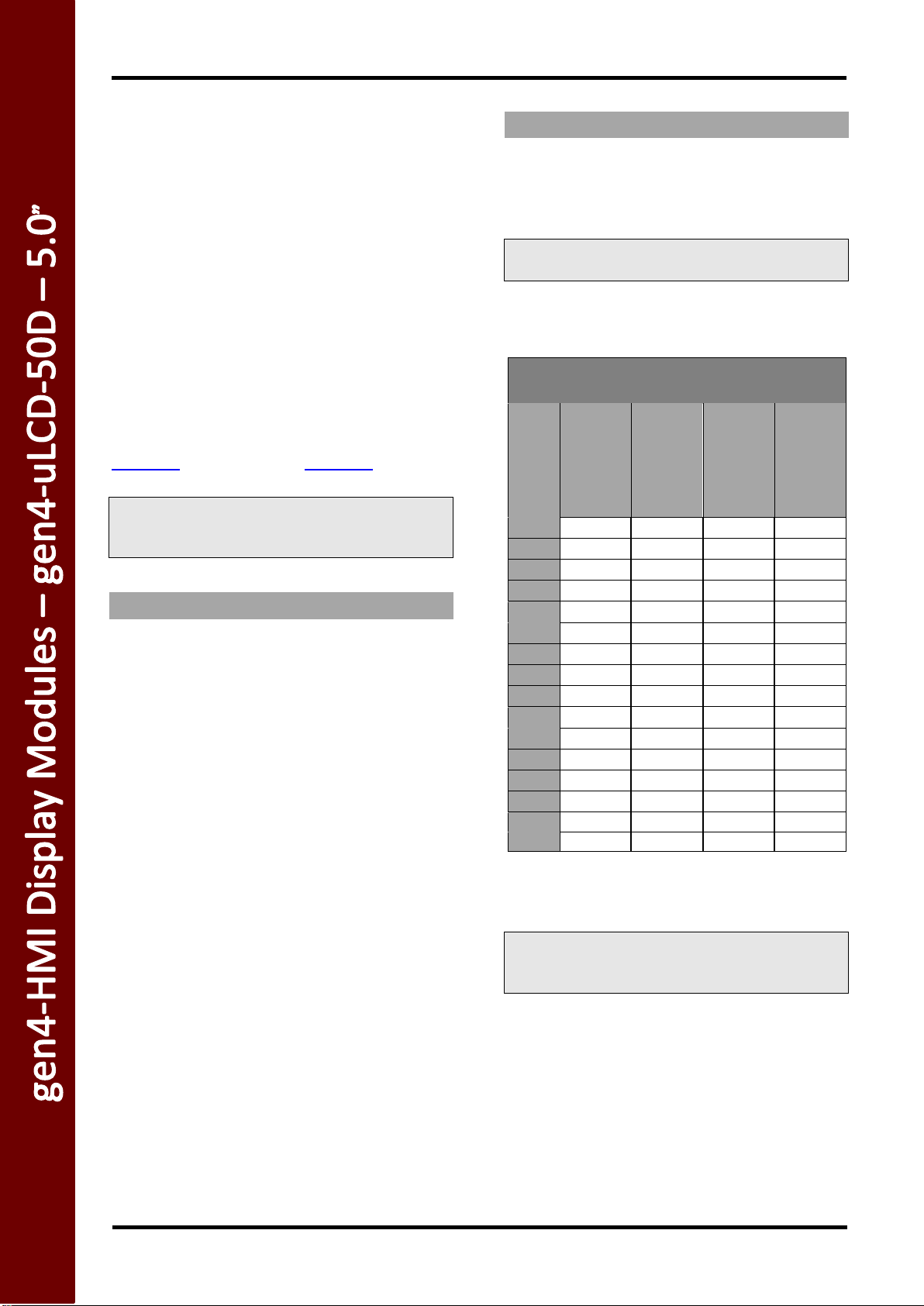
ABSOLUTE MAXIMUM RATINGS
Operating ambient temperature ................................................................................................... -20°C to +70°C
Storage temperature ...................................................................................................................... -30°C to +80°C
Voltage on any digital input pin with respect to GND ....................................................................... -0.3V to 6.0V
Voltage on VCC with respect to GND ................................................................................................. -0.3V to 6.0V
Maximum current sunk/sourced by any pin .............................................................................................. 10.0mA
Maximum current sunk/sourced by all ports ........................................................................................... 200.0mA
NOTE: Stresses above those listed here may cause permanent damage to the device. This is a stress rating only
and functional operation of the device at those or any other conditions above those indicated in the
recommended operation listings of this specification is not implied. Exposure to maximum rating conditions for
extended periods may affect device reliability.
RECOMMENDED OPERATING CONDITIONS
Parameter
Conditions
Min
Typ
Max
Units
Supply Voltage (VCC)
Stable external supply required
4.0
5.0
5.5
V
Processor voltage (VP)
--
3.3
--
V
Operating Temperature
-10
--
+60
°C
Input Low Voltage (VIL)
all pins 0 --
0.2VP
V
Input High Voltage (VIH)
non 5V tolerant pins
0.8VP
--
3.3
V
Input High Voltage (VIH)
PA4-PA13, RX0 and TX0 pins
0.8VP
--
5.5
V
Reset Pulse
External Open Collector
2.0
--
--
µs
Operational Delay
Power-Up or External Reset
500
--
3000
ms
GLOBAL CHARACTERISTICS BASED ON OPERATING CONDITIONS
Parameter
Conditions
Min
Typ
Max
Units
Supply Current (ICC)
gen4-uLCD-50D (Contrast = 15)
--
440
--
mA
gen4-uLCD-50D-CLB (Contrast = 15)
--
440
--
mA
gen4-uLCD-50DT (Contrast = 15)
--
440
--
mA
gen4-uLCD-50DCT-CLB (Contrast = 15)
--
445
--
mA
gen4-uLCD-50D-SB (Contrast = 15)
--
600
--
mA
gen4-uLCD-50D-CLB-SB (Contrast = 15)
--
600
--
mA
gen4-uLCD-50DT-SB (Contrast = 15)
--
600
--
mA
gen4-uLCD-50DCT-CLB-SB (Contrast = 15)
--
610
--
mA
Display Endurance
Hours of operation, measured to
when display is 50% original
brightness
30000
--
--
H
Touch Screen Endurance
(Resistive Touch)
Number of touches/hits with a
12.5mm tip at a rate of 2x per
second with 250gf force
--
1M
--
Touches
Slide stylus on screen, 100gf force,
60mm/s speed with a 0.8mm
polyacetal tip stylus pen
--
100K
--
Slides
18. Specifications
gen4-HMI Display Modules
gen4-uLCD-50D Page 26 of 29 www.4dsystems.com.au
Page 27

gen4-HMI Display Modules
Touch Screen Transparency
Resistive Touch
82
--
--
%
Capacitive Touch
90
--
--
%
Touch Screen Operational
Force (Resistive Touch)
Only use Finger or Stylus, do not
use anything sharp or metal
20
--
100
Gf
CLB Hardness
Cover Lens Bezel Glass Hardness
-- 6 --
H
LCD DISPLAY INFORMATION
Parameter
Conditions
Specification
Display Type TFT Transmissive LCD
Display Size 5.0” Diagonal
Display Resolution
800 x 480 (Landscape/Wide Viewing)
Display Brightness
gen4-uLCD-50D (Contrast = 15)
500 cd/m2
gen4-uLCD-50D-CLB (Contrast = 15)
485 cd/m2
gen4-uLCD-50DT (Contrast = 15)
400 cd/m2
gen4-uLCD-50DCT-CLB (Contrast = 15)
475 cd/m2
gen4-uLCD-50D-SB (Contrast = 15)
820 cd/m2
gen4-uLCD-50D-CLB-SB (Contrast = 15)
735 cd/m2
gen4-uLCD-50DT-SB (Contrast = 15)
650 cd/m2
gen4-uLCD-50DCT-CLB-SB (Contrast =
15)
705 cd/m2
Display Contrast Ratio
Typical
500:1
Display Viewing Angles
Above Centre
70 Degrees
Below Centre
50 Degrees
Left of Centre
70 Degrees
Right of Centre
70 Degrees
Display Viewing Direction
12 o’clock Display
(Optimal viewing is from above when in
Landscape/Wide mode)
Display Backlighting
gen4-uLCD-50Dxx-xxx Models
2x6 Parallel LED’s
gen4-uLCD-50Dxx-xxx-SB Models
3x6 Parallel LED’s
Pixel Pitch
0.135 x 0.135mm (Square pixels)
Pixel Density
Number of pixels in 1 row in
25.4mm
183 DPI/PPI
gen4-uLCD-50D Page 27 of 29 www.4dsystems.com.au
Page 28

Revision
Number
Date
Description
1.2
xx/10/2015
Initial Public Release Version
1.3
xx/03/2017
SB3 and R12 were added to be able to power up 7” SB Displays, existing
SB3 was renamed to SB4
1.5
xx/02/2019
Filters were added for better resistance to EMI/RF, CE-EMC certified
1.5
01/04/2019
Component Change Only - Regulator U3 changed to AP7361C-33ER-13
Revision
Number
Date
Description
0.1
xx/xx/2015
Internal Use Only
1.0
10/12/2015
Initial Public Release Version
1.1
22/12/2015
Cosmetic Changes to gen4 Datasheet range
1.2
13/06/2016
Drawing and Specification updates, other minor changes
1.3
28/09/2016
Addition of Super Bright variant information
1.4
05/05/2017
Addition of HW REV 1.2 and REV 1.3 schematics
1.5
17/10/2017
Addition of processor voltage information
1.6
09/04/2018
Addition of 4D-UPA
1.7
04/03/2019
Cosmetic Changes to gen4 Datasheet range, added HW REV 1.5 Schematics
1.8
05/08/2019
Updated the REV 1.5 Schematics
19. Hardware Revision History
20. Datasheet Revision History
gen4-HMI Display Modules
gen4-uLCD-50D Page 28 of 29 www.4dsystems.com.au
Page 29

gen4-HMI Display Modules
21. Legal Notice
Proprietary Information
The information contained in this document is the property of 4D Systems Pty. Ltd. and may be the subject of patents
pending or granted, and must not be copied or disclosed without prior written permission.
4D Systems endeavours to ensure that the information in this document is correct and fairly stated but does not
accept liability for any error or omission. The development of 4D Systems products and services is continuous and
published information may not be up to date. It is important to check the current position with 4D Systems. 4D
Systems reserves the right to modify, update or makes changes to Specifications or written material without prior
notice at any time.
All trademarks belong to their respective owners and are recognised and acknowledged.
Disclaimer of Warranties & Limitation of Liability
4D Systems makes no warranty, either expressed or implied with respect to any product, and specifically disclaims all
other warranties, including, without limitation, warranties for merchantability, non-infringement and fitness for any
particular purpose.
Information contained in this publication regarding device applications and the like is provided only for your
convenience and may be superseded by updates. It is your responsibility to ensure that your application meets with
your specifications.
Images and graphics used throughout this document are for illustrative purposes only. All images and graphics used
are possible to be displayed on the 4D Systems range of products, however the quality may vary.
In no event shall 4D Systems be liable to the buyer or to any third party for any indirect, incidental, special,
consequential, punitive or exemplary damages (including without limitation lost profits, lost savings, or loss of
business opportunity) arising out of or relating to any product or service provided or to be provided by 4D Systems,
or the use or inability to use the same, even if 4D Systems has been advised of the possibility of such damages.
4D Systems products are not fault tolerant nor designed, manufactured or intended for use or resale as on line control
equipment in hazardous environments requiring fail – safe performance, such as in the operation of nuclear facilities,
aircraft navigation or communication systems, air traffic control, direct life support machines or weapons systems in
which the failure of the product could lead directly to death, personal injury or severe physical or environmental
damage (‘High Risk Activities’). 4D Systems and its suppliers specifically disclaim any expressed or implied warranty
of fitness for High Risk Activities.
Use of 4D Systems’ products and devices in 'High Risk Activities' and in any other application is entirely at the buyer’s
risk, and the buyer agrees to defend, indemnify and hold harmless 4D Systems from any and all damages, claims, suits,
or expenses resulting from such use. No licenses are conveyed, implicitly or otherwise, under any 4D Systems
intellectual property rights.
22. Contact Information
For Technical Support: www.4dsystems.com.au/support
For Sales Support: sales@4dsystems.com.au
Website: www.4dsystems.com.au
Copyright 4D Systems Pty. Ltd. 2000-2019.
gen4-uLCD-50D Page 29 of 29 www.4dsystems.com.au
Page 30

Mouser Electronics
Authorized Distributor
Click to View Pricing, Inventory, Delivery & Lifecycle Information:
4D Systems:
SK-gen4-50DT-AR SK-gen4-50D-AR gen4-uLCD-50D gen4-uLCD-50D-AR SK-gen4-50DT-PI SK-gen4-50D-PI
gen4-uLCD-50DT-PI gen4-uLCD-50DT SK-gen4-50D gen4-uLCD-50D-PI gen4-uLCD-50DT-AR SK-gen4-50DT
gen4-uLCD-50DCT-CLB-PI gen4-uLCD-50D-SB-AR gen4-uLCD-50DCT-CLB-SB SK-gen4-50D-CLB-AR SK-gen450DT-SB-AR gen4-uLCD-50D-CLB-SB gen4-uLCD-50DT-SB-AR gen4-uLCD-50D-CLB-AR gen4-uLCD-50DCT-CLBSB-PI SK-gen4-50D-SB-AR gen4-uLCD-50D-CLB-SB-PI gen4-uLCD-50DT-SB SK-gen4-50D-CLB-SB-PI SK-gen450D-SB-PI SK-gen4-50DCT-CLB-SB-AR gen4-uLCD-50DCT-CLB gen4-uLCD-50D-SB gen4-uLCD-50D-CLB SKgen4-50DT-SB SK-gen4-50DCT-CLB-AR SK-gen4-50DT-SB-PI SK-gen4-50DCT-CLB-SB-PI SK-gen4-50D-SB SKgen4-50DCT-CLB-PI SK-gen4-50D-CLB-SB-AR gen4-uLCD-50DCT-CLB-AR SK-gen4-50DCT-CLB-SB gen4-uLCD50D-CLB-PI gen4-uLCD-50D-CLB-SB-AR gen4-uLCD-50DT-SB-PI SK-gen4-50DCT-CLB SK-gen4-50D-CLB-PI
gen4-uLCD-50DCT-CLB-SB-AR SK-gen4-50D-CLB SK-gen4-50D-CLB-SB gen4-uLCD-50D-SB-PI
 Loading...