


Yobon YB1253ST23X120, YB1253ST23X130, YB1253ST23X140, YB1253ST23X150, YB1253ST23X160 Schematic [ru]
...YB1253
300mA, Low Power, High PSRR LDO Regulator
Description
The YB1253 is a series of ultra-low-noise, high PSRR, and low quiescent current low dropout (LDO) linear regulators with 2.0% output voltage accuracy. The YB1253 regulators achieve a low 300mA dropout at
300mA load current of 3.6V output and are available in voltages ranging from 1.2V to 3.6V with 0.1 V per step (custom voltage is considerate at request).
The YB1253 regulators are optimized to work with low-ESR and low cost ceramic capacitors, reducing the amount of board space critical in portable devices. The
YB1253 requires only 1.0μF output capacitor for stability with any load and consumes less than 1μA in shutdown mode.
Built-in thermal shutdown and short-circuit current limit offer secure protection against fault operation. YB1253 regulators also include an auto-discharge function. The
YB1253 regulators are available in SOT-23
/ SOT-25 / SOT-89 packages.
Features
•High Accuracy Output Voltage : + 2%
•Wide Output Voltage Range : 1.2~3.6V
•Ultra-Low-Noise Low-Drop-Out
•Typical Output Current : 300 mA
•Low Quiescent Current: ~10μA
•300mV Dropout at 300mA 3.6V Output
•Stable with 1.0μF Ceramic Capacitor
•Only Need Input and Output Capacitors
•Thermal Protection Shutdown
•Auto discharge function
•Green Package (RoHS) Available
Applications
•PDA, Notebook, PC Computers
•DSC, Cellular phones
•PCMCIA Cards, PC Cameras
•USB Based Portable Devices
•GSM/GPRS/3G RF Transceiver
•Wireless LANs
•Bluetooth Portable Radios
•Battery-Powered Devices
Typical Application Circuitry
Input |
|
|
Input |
VIN VOUT |
Output |
|
VIN |
VOUT |
Output |
|
|||
|
|
|||||
|
Cin=1uF |
YB1253 |
Cout=1uF |
|||
Cin=1uF |
YB1253 |
|||||
Cout=1uF |
|
|
||||
ON |
EN |
|
|
GND |
|
|
|
|
|
|
|||
OFF |
|
GND |
|
|
|
|
Figure 1-2 : SOT-23 application circuit
Figure 1-1 : SOT-25 application circuit
YB1253 Rev. 1.5 |
www.yobon.com.tw |
1 |
YB1253
300mA, Low Power, High PSRR LDO Regulator
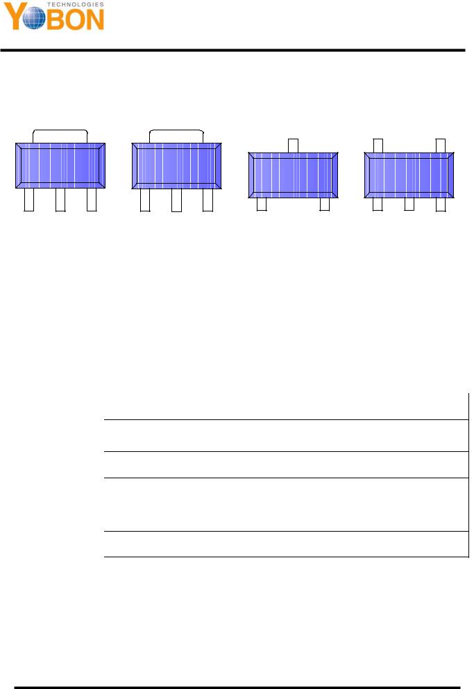
Pin Configuration
|
SOT-89 |
|
SOT-89R |
|
|
1 |
2 |
3 |
1 |
2 |
3 |
GND |
VIN |
VOUT |
VOUT |
GND |
VIN |
VIN |
|
VOUT |
|
NC |
3 |
|
5 |
|
4 |
SOT-23 |
|
|
SOT-25 |
|
1 |
2 |
1 |
2 |
3 |
GND |
VOUT |
VIN |
GND |
EN |
Figure 2 : pin configuration
Pin Description
Table 1
Pin Name |
Pin Function |
|
Unregulated Input Supply. Bypass with a capacitor to GND |
VIN |
|
|
|
GND |
Ground pin |
|
|
EN |
Pull high to enable the regulator |
|
|
NC |
No connection is required |
|
|
VOUT |
Regulated Output Voltage |
|
|
YB1253 Rev. 1.5 |
www.yobon.com.tw |
2 |

YB1253
300mA, Low Power, High PSRR LDO Regulator
Ordering Information
Y B 1253 |
X |
O utput V oltage 120 : 1.2V
130 : 1.3V
:
360 : 3.6V
X : fixed
P ackage Type
S T23 : S O T -23
S T25 : S O T -25
S T89 : S O T -89
S T8R : S O T -89R
*O rder exam ple :
Y B 1253 S T89X 250 for Y B 1253 of 2.5V output and S O T-89 package *S hipping Q uantity :
S O T -23 |
: 3000 |
units tape & reel |
S O T -25 |
: 3000 |
units tape & reel |
S O T -89 |
: 1000 |
units tape & reel |
S O T -89R |
: 1000 units tape & reel |
|
*O nly green package
Marking Information
Absolute Maximum Ratings (Note 1) |
Recommended Operating Conditions |
|
(Note 2) |
Supply Voltage ................................ |
-0.3V to 6.0V |
Output Voltage ....................... |
-0.3V to (VIN+0.3V) |
Output Short-Circuit Duration.................... |
Infinite |
Junction Temperature Range................... |
+150 |
Storage Temperature Range...... |
-65 to +150 |
Lead Temperature.................................... |
+250 |
ESD Susceptibility (HBM)…………… ………2KV
ESD Susceptibility (MM) ............................. |
200V |
Note: |
|
Input Supply Voltage......................... |
2V to 5.5V |
Operating Temperature.............. |
-40 to +85 |
Thermal Information |
(Note 3) |
Thermal Resistance (SOT-23/25, θJA).280 /W
Thermal Resistance (SOT-89, θJA)…...180 /W
InternalPowerDissipation (SOT-23/25,PD)……0.4W
Internal Power Dissipation (SOT-89, PD)0.55W
1.Exceeding these ratings may damage the device.
2.The device is not guaranteed to function outside of its operating conditions.
3.θJA is measured in free air at TA = 25 on a low effective thermal conductivity board.
YB1253 Rev. 1.5 |
www.yobon.com.tw |
3 |

YB1253
300mA, Low Power, High PSRR LDO Regulator
Electrical Characteristics
Table 2
TA = 25 , VIN = ( VOUT + 1 V ), CIN = COU T = 1.0μF, VEN = VIN, unless otherwise
Function Parameter |
Conditions |
Min |
Typ |
Max |
Units |
|
|
|
|
|
|
Input Voltage Range |
|
2.0 |
|
5.5 |
V |
|
|
|
|
|
|
Output Voltage, VOUT |
Predefined |
1.2 |
|
3.6 |
V |
|
|
|
|
|
|
Output Voltage Accuracy |
IOUT = 10mA, VOUT >= 1.3V |
-2.0 |
|
+2.0 |
% |
|
|
|
|
|
|
IOUT = 10mA, VOUT = 1.2V |
0 |
|
+4.0 |
% |
|
|
|
||||
|
|
|
|
|
|
Output Current Limit |
Short-circuit output |
|
500 |
|
mA |
|
|
|
|
|
|
|
Vout = 3.6V, Iout = 300 mA |
|
300 |
|
|
|
|
|
|
|
|
|
Vout = 3.3V, Iout = 300 mA |
|
350 |
|
|
Dropout Voltage (Note 1) |
|
|
|
|
mV |
Vout = 2.8V, Iout = 300 mA |
|
430 |
|
||
|
|
|
|
|
|
|
Vout = 1.8V, Iout = 300 mA |
|
600 |
|
|
|
|
|
|
|
|
|
Vout = 1.2V, Iout = 300 mA |
|
900 |
|
|
|
|
|
|
|
|
Ground Current |
Iground = Iin - Iout |
|
10 |
|
μA |
|
|
|
|
|
|
Line Regulation |
Vin = (Vout+1V) to 5.5V, Iout =10mA |
|
0.10 |
0.20 |
%/V |
|
|
|
|
|
|
Load Regulation |
Iout = 1mA to 300 mA |
|
0.005 |
0.01 |
%/mA |
|
|
|
|
|
|
Shutdown Supply Current |
EN = Vin=0V |
|
|
1 |
μA |
|
|
|
|
|
|
Ripple Rejection (PSRR) |
(Note 2) |
|
50 |
|
dB |
|
|
|
|
|
|
Start Up Delay (Note 3) |
Rload=100ohm |
|
200 |
|
μS |
|
|
|
|
|
|
Shutdown Delay |
Rload=10K ohm, VOUT=1.5V |
|
1 |
|
mS |
|
|
|
|
|
|
Rload=10K ohm, VOUT=1.2V |
|
1 |
|
mS |
|
|
|
|
|||
|
|
|
|
|
|
EN Logic Low Level |
Vin = 2.0V to 5.5V |
|
|
0.4 |
V |
|
|
|
|
|
|
EN Logic High Level |
Vin = 2.0V to 5.5V |
1.2 |
|
Vin |
V |
|
|
|
|
|
|
EN Input Bias Current |
Vin = EN = 3V |
|
1.5 |
|
μA |
|
|
|
|
|
|
Thermal Shutdown |
Shutdown Temperature |
|
160 |
|
°C |
|
|
|
|
|
|
Thermal Hysteresis |
|
|
20 |
|
°C |
|
|
|
|
|
|
Note 1: The dropout voltage varies depending on output voltage selection. Dropout is defined as VIN–VOUT when VOUT is 100mV below nominal VOUT where Vin=Vout + 1V for nominal VOUT.
Note 2: PSRR is tested at Vin=3.8+1Vppac, Vout=2.8V, I_load=1mA. Note 3: Time needed for VOUT to reach 90% of final value.
YB1253 Rev. 1.5 |
www.yobon.com.tw |
4 |
 Loading...