


XILINX XCS40-4PQ240C, XCS40-4PQ208C, XCS40-4BG256C, XCS40-3PQ240C, XCS40-3PQ208I Datasheet
...R
Spartan and Spartan-XL Families
Field Programmable Gate Arrays
DS060 (v1.6) September 19, 2001 |
Product Specification |
|
|
Introduction
The Spartan™ and the Spartan-XL families are a high-vol- ume production FPGA solution that delivers all the key requirements for ASIC replacement up to 40,000 gates. These requirements include high performance, on-chip RAM, core solutions and prices that, in high volume, approach and in many cases are equivalent to mask programmed ASIC devices.
The Spartan series is the result of more than 14 years of FPGA design experience and feedback from thousands of customers. By streamlining the Spartan series feature set, leveraging advanced process technologies and focusing on total cost management, the Spartan series delivers the key features required by ASIC and other high-volume logic users while avoiding the initial cost, long development cycles and inherent risk of conventional ASICs. The Spartan and Spartan-XL families in the Spartan series have ten members, as shown in Table 1.
Spartan and Spartan-XL Features
Note: The Spartan series devices described in this data sheet include the 5V Spartan family and the 3.3V Spartan-XL family. See the separate data sheet for the 2.5V Spartan-II family.
•First ASIC replacement FPGA for high-volume production with on-chip RAM
•Density up to 1862 logic cells or 40,000 system gates
•Streamlined feature set based on XC4000 architecture
•System performance beyond 80 MHz
•Broad set of AllianceCORE™ and LogiCORE™ predefined solutions available
•Unlimited reprogrammability
•Low cost
•System level features
-Available in both 5V and 3.3V versions
- On-chip SelectRAM™ memory
-Fully PCI compliant
-Full readback capability for program verification and internal node observability
-Dedicated high-speed carry logic
-Internal 3-state bus capability
-Eight global low-skew clock or signal networks
-IEEE 1149.1-compatible Boundary Scan logic
-Low cost plastic packages available in all densities
-Footprint compatibility in common packages
•Fully supported by powerful Xilinx development system
-Foundation Series: Integrated, shrink-wrap software
-Alliance Series: Dozens of PC and workstation third party development systems supported
-Fully automatic mapping, placement and routing
Additional Spartan-XL Features
•3.3V supply for low power with 5V tolerant I/Os
•Power down input
•Higher performance
•Faster carry logic
•More flexible high-speed clock network
•Latch capability in Configurable Logic Blocks
•Input fast capture latch
•Optional mux or 2-input function generator on outputs
•12 mA or 24 mA output drive
•5V and 3.3V PCI compliant
•Enhanced Boundary Scan
•Express Mode configuration
•Chip scale packaging
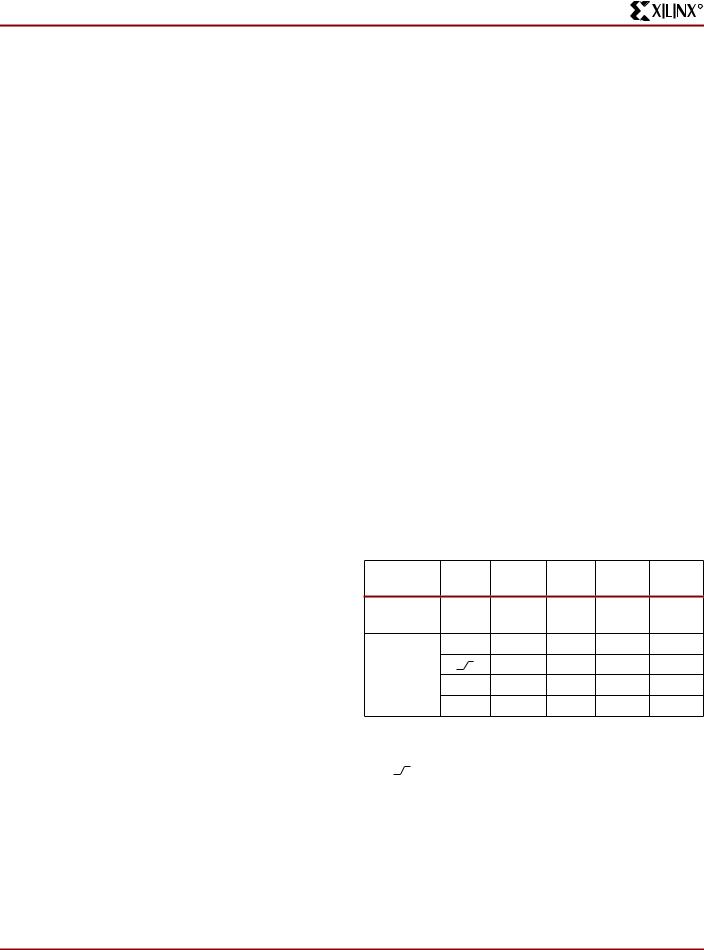
Table 1: Spartan and Spartan-XL Field Programmable Gate Arrays
|
Logic |
Max |
Typical |
|
|
|
Max. |
Total |
|
System |
Gate Range |
CLB |
Total |
No. of |
Avail. |
Distributed |
|
|
|
|||||||
Device |
Cells |
Gates |
(Logic and RAM)(1) |
Matrix |
CLBs |
Flip-flops |
User I/O |
RAM Bits |
XCS05 and XCS05XL |
238 |
5,000 |
2,000-5,000 |
10 x 10 |
100 |
360 |
77 |
3,200 |
|
|
|
|
|
|
|
|
|
XCS10 and XCS10XL |
466 |
10,000 |
3,000-10,000 |
14 x 14 |
196 |
616 |
112 |
6,272 |
|
|
|
|
|
|
|
|
|
XCS20 and XCS20XL |
950 |
20,000 |
7,000-20,000 |
20 x 20 |
400 |
1,120 |
160 |
12,800 |
|
|
|
|
|
|
|
|
|
XCS30 and XCS30XL |
1368 |
30,000 |
10,000-30,000 |
24 x 24 |
576 |
1,536 |
192 |
18,432 |
|
|
|
|
|
|
|
|
|
XCS40 and XCS40XL |
1862 |
40,000 |
13,000-40,000 |
28 x 28 |
784 |
2,016 |
224 |
25,088 |
|
|
|
|
|
|
|
|
|
Notes:
1.Max values of Typical Gate Range include 20-30% of CLBs used as RAM.
© 2001 Xilinx, Inc. All rights reserved. All Xilinx trademarks, registered trademarks, patents, and disclaimers are as listed a t http://www.xilinx.com/legal.htm. All other trademarks and registered trademarks are the property of their respective owners. All specifications are subject to change without notice.
DS060 (v1.6) September 19, 2001 |
www.xilinx.com |
1 |
Product Specification |
1-800-255-7778 |
|
Spartan and Spartan-XL Families Field Programmable Gate Arrays
R
General Overview
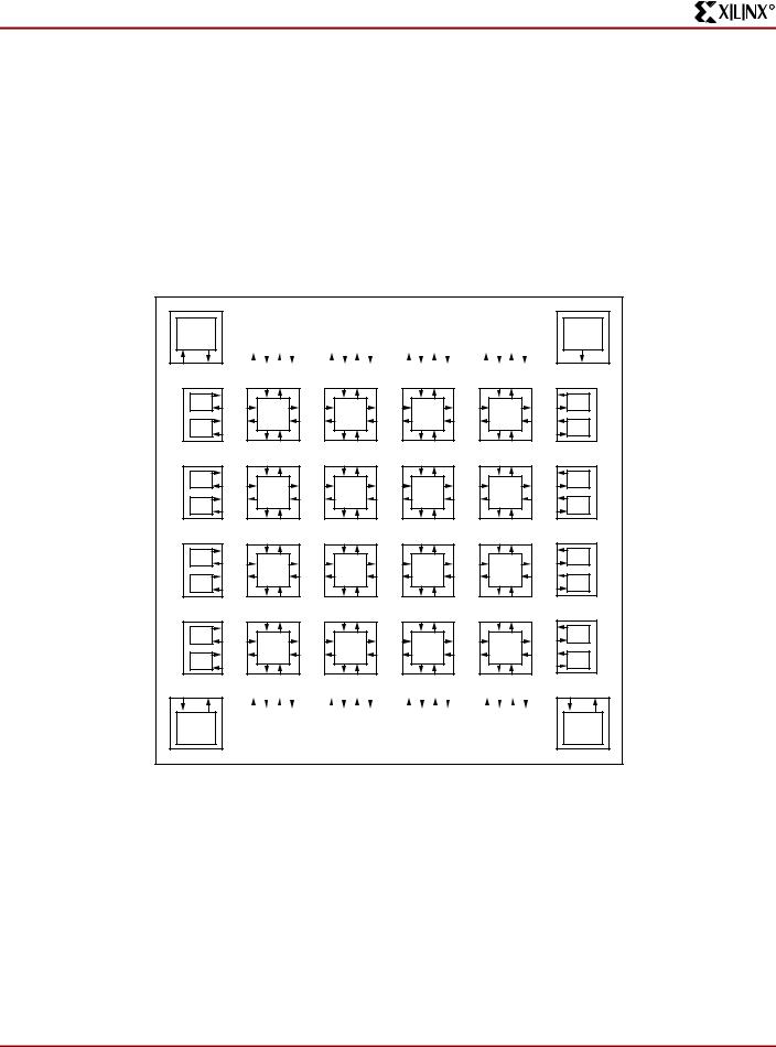
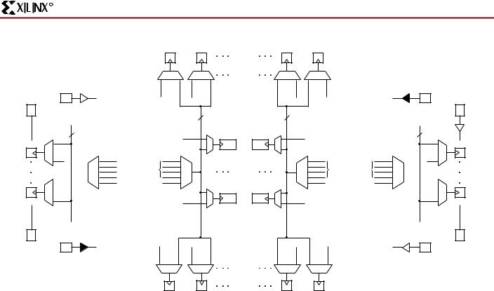
Spartan series FPGAs are implemented with a regular, flexible, programmable architecture of Configurable Logic Blocks (CLBs), interconnected by a powerful hierarchy of versatile routing resources (routing channels), and surrounded by a perimeter of programmable Input/Output Blocks (IOBs), as seen in Figure 1. They have generous routing resources to accommodate the most complex interconnect patterns.
The devices are customized by loading configuration data into internal static memory cells. Re-programming is possible an unlimited number of times. The values stored in these
memory cells determine the logic functions and interconnections implemented in the FPGA. The FPGA can either actively read its configuration data from an external serial PROM (Master Serial mode), or the configuration data can be written into the FPGA from an external device (Slave Serial mode).
Spartan series FPGAs can be used where hardware must be adapted to different user applications. FPGAs are ideal for shortening design and development cycles, and also offer a cost-effective solution for production rates well beyond 50,000 systems per month.
B- |
SCAN |
IOB |
IOB |
IOB |
IOB |
IOB |
IOB |
IOB |
IOB |
RDBK |
|
|
|
|
|
|
|
|
|
|
|
IOB |
|
|
IOB |
|
||
|
|
|
|
|
|
|
|
|
CLB |
CLB |
CLB |
CLB |
|
|
|
|
|
|
|
|
|
|
|
IOB |
|
|
IOB |
|
||
|
|
|
|
|
|
|
|
|
|
|
|
|
|
|
|
|
|
|
|
|
|
|
|
|
|
|
|
|
IOB |
|
|
IOB |
|
|
|
|
IOB |
|
|
IOB |
|
|||
|
|
|
|
|
|
|
|
|
|
|
|
|
|
|
|
|
|
CLB |
CLB |
CLB |
CLB |
Routing Channels
CLB |
CLB |
CLB |
CLB |
|
|
|
|
|
|
|
|
|
|
|
|
|
|
|
|
|
|
|
|
|
IOB |
|
|
IOB |
|
|
|
|
IOB |
|
|
|
IOB |
|
|||
|
|
|
|
|
|
|
|
|
|
|
|
|
|
|
|
|
|
|
VersaRing Routing Channels
|
|
|
|
|
|
|
|
|
|
|
IOB |
|
|
IOB |
|
||
|
|
|
|
|
|
|
|
|
CLB |
CLB |
CLB |
CLB |
|
|
|
|
|
|
|
|
|
|
|
IOB |
|
|
IOB |
|
||
|
|
|
|
|
|
|
|
|
OSC |
IOB |
IOB |
IOB |
IOB |
IOB |
IOB |
IOB |
IOB |
START |
-UP |
DS060_01_081100
Figure 1: Basic FPGA Block Diagram
2 |
www.xilinx.com |
DS060 (v1.6) September 19, 2001 |
|
1-800-255-7778 |
Product Specification |

R
Spartan and Spartan-XL Families Field Programmable Gate Arrays
Spartan series devices achieve high-performance, low-cost operation through the use of an advanced architecture and semiconductor technology. Spartan and Spartan-XL devices provide system clock rates exceeding 80 MHz and internal performance in excess of 150 MHz. In contrast to other FPGA devices, the Spartan series offers the most cost-effective solution while maintaining leading-edge performance. In addition to the conventional benefit of high volume programmable logic solutions, Spartan series FPGAs also offer on-chip edge-triggered single-port and dual-port RAM, clock enables on all flip-flops, fast carry logic, and many other features.
The Spartan/XL families leverage the highly successful XC4000 architecture with many of that family’s features and benefits. Technology advancements have been derived from the XC4000XLA process developments.
Logic Functional Description
The Spartan series uses a standard FPGA structure as shown in Figure 1, page 2. The FPGA consists of an array of configurable logic blocks (CLBs) placed in a matrix of routing channels. The input and output of signals is achieved through a set of input/output blocks (IOBs) forming a ring around the CLBs and routing channels.
•CLBs provide the functional elements for implementing the user’s logic.
•IOBs provide the interface between the package pins and internal signal lines.
•Routing channels provide paths to interconnect the inputs and outputs of the CLBs and IOBs.
The functionality of each circuit block is customized during configuration by programming internal static memory cells. The values stored in these memory cells determine the logic functions and interconnections implemented in the FPGA.
Configurable Logic Blocks (CLBs)
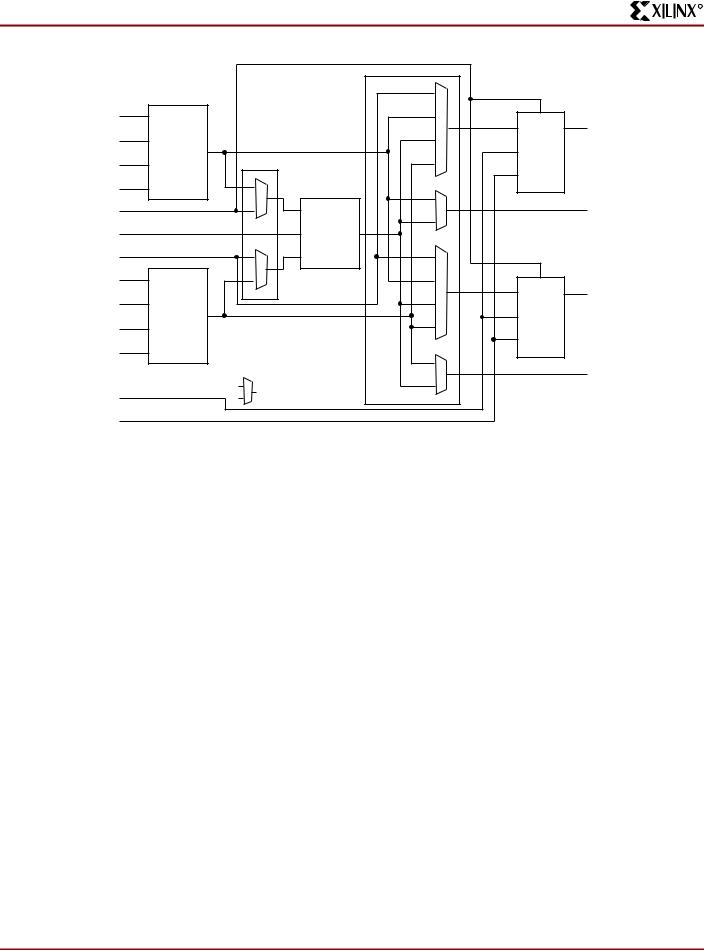
The CLBs are used to implement most of the logic in an FPGA. The principal CLB elements are shown in the simplified block diagram in Figure 2. There are three look-up tables (LUT) which are used as logic function generators, two flip-flops and two groups of signal steering multiplexers. There are also some more advanced features provided by the CLB which will be covered in the Advanced Features Description, page 13.
Function Generators
Two 16 x 1 memory look-up tables (F-LUT and G-LUT) are used to implement 4-input function generators, each offering unrestricted logic implementation of any Boolean function of up to four independent input signals (F1 to F4 or G1 to G4). Using memory look-up tables the propagation delay is independent of the function implemented.
A third 3-input function generator (H-LUT) can implement any Boolean function of its three inputs. Two of these inputs are controlled by programmable multiplexers (see box "A" of Figure 2). These inputs can come from the F-LUT or G-LUT outputs or from CLB inputs. The third input always comes from a CLB input. The CLB can, therefore, implement certain functions of up to nine inputs, like parity checking. The three LUTs in the CLB can also be combined to do any arbitrarily defined Boolean function of five inputs.
DS060 (v1.6) September 19, 2001 |
www.xilinx.com |
3 |
Product Specification |
1-800-255-7778 |
|
Spartan and Spartan-XL Families Field Programmable Gate Arrays
R
|
G-LUT |
|
|
|
B |
|
|
|
|
|
|
|
|
|
|
G4 |
G4 |
|
|
|
|
SR |
|
|
Logic |
|
|
|
D |
Q |
YQ |
G3 |
|
|
|
|
|
|
|
G3 Function |
|
|
|
|
|
||
|
of |
G |
|
|
CK |
|
|
G2 |
G2 G1-G4 |
|
|
|
EC |
|
|
|
|
|
|
|
|
|
|
G1 |
G1 |
|
H-LUT |
|
|
|
|
SR |
|
G |
|
Logic |
|
|
Y |
|
|
|
|
|
|
|
|
H1 |
|
|
Function |
H |
|
|
|
|
H1 |
of |
|
|
|||
|
|
|
|
|
|
|
|
DIN |
|
F |
|
F-G-H1 |
|
|
|
|
|
|
|
|
|
||
F4 |
F4 |
A |
|
|
|
SR |
|
F3 |
Logic |
|
|
D |
Q |
XQ |
|
F3 Function |
|
|
|
|
|
||
|
of |
G |
|
|
CK |
|
|
F2 |
F2 F1-F4 |
|
|
|
EC |
|
|
|
|
|
|
|
|
|
|
F1 |
F1 |
|
|
|
|
|
|
|
F-LUT |
|
|
|
|
|
X |
|
|
Multiplexer Controlled |
|
|
|
||
K |
|
by Configuration Program |
|
|
|||
EC |
|
|
|
|
|
DS060_02_0506 01 |
|
|
|
|
|
|
|
||
Figure 2: Spartan/XL Simplified CLB Logic Diagram (some features not shown)
A CLB can implement any of the following functions:
•Any function of up to four variables, plus any second function of up to four unrelated variables, plus any third function of up to three unrelated variables
Note: When three separate functions are generated, one of the function outputs must be captured in a flip-flop internal to the CLB. Only two unregistered function generator outputs are available from the CLB.
•Any single function of five variables
•Any function of four variables together with some functions of six variables
•Some functions of up to nine variables.
Implementing wide functions in a single block reduces both the number of blocks required and the delay in the signal path, achieving both increased capacity and speed.
The versatility of the CLB function generators significantly improves system speed. In addition, the design-software tools can deal with each function generator independently. This flexibility improves cell usage.
Flip-Flops
Each CLB contains two flip-flops that can be used to register (store) the function generator outputs. The flip-flops and function generators can also be used independently (see Figure 2). The CLB input DIN can be used as a direct input to either of the two flip-flops. H1 can also drive either flip-flop via the H-LUT with a slight additional delay.
The two flip-flops have common clock (CK), clock enable (EC) and set/reset (SR) inputs. Internally both flip-flops are also controlled by a global initialization signal (GSR) which is described in detail in Global Signals: GSR and GTS, page 20.
Latches (Spartan-XL only)
The Spartan-XL CLB storage elements can also be configured as latches. The two latches have common clock (K) and clock enable (EC) inputs. Functionality of the storage element is described in Table 2.
4 |
www.xilinx.com |
DS060 (v1.6) September 19, 2001 |
|
1-800-255-7778 |
Product Specification |

R
Spartan and Spartan-XL Families Field Programmable Gate Arrays
.
Table 2: CLB Storage Element Functionality
Mode |
CK |
EC |
SR |
D |
|
Q |
||
|
|
|
|
|
|
|
|
|
Power-Up or |
|
X |
X |
X |
X |
|
SR |
|
GSR |
|
|
|
|
|
|
|
|
|
|
|
|
|
|
|
|
|
Flip-Flop |
|
X |
X |
1 |
X |
|
SR |
|
Operation |
|
|
|
|
|
|
|
|
|
|
|
1* |
0* |
D |
|
D |
|
|
|
|
|
|
||||
|
|
|
|
|
|
|
|
|
|
0 |
|
X |
0* |
X |
|
Q |
|
|
|
|
|
|
|
|
|
|
Latch |
1 |
|
1* |
0* |
X |
|
Q |
|
Operation |
|
|
|
|
|
|
|
|
0 |
|
1* |
0* |
D |
|
D |
||
(Spartan-XL) |
|
|
||||||
|
|
|
|
|
|
|
|
|
|
|
|
|
|
|
|
|
|
Both |
|
X |
0 |
0* |
X |
|
Q |
|
|
|
|
|
|
|
|
|
|
Legend: |
|
|
|
|
|
|
|
|
X |
Don’t care |
|
|
|
|
|||
|
Rising edge (clock not inverted). |
|
||||||
SR |
Set or Reset value. Reset is default. |
|||||||
0* |
Input is Low or unconnected (default |
|||||||
|
value) |
|
|
|
|
|
||
1* |
Input is High or unconnected (default |
|||||||
|
value) |
|
|
|
|
|
||
|
SR |
|
|
|
GND |
|
|
|
GSR |
|
|
|
|
SD |
|
D |
D |
Q |
Q |
CK |
|
|
|
|
|
RD |
|
EC |
|
|
|
|
Vcc |
|
|
Multiplexer Controlled
by Configuration Program
DS060_03_041901
Figure 3: CLB Flip-Flop Functional Block Diagram
Clock Input
Each flip-flop can be triggered on either the rising or falling clock edge. The CLB clock line is shared by both flip-flops. However, the clock is individually invertible for each flip-flop (see CK path in Figure 3). Any inverter placed on the clock line in the design is automatically absorbed into the CLB.
Clock Enable
The clock enable line (EC) is active High. The EC line is shared by both flip-flops in a CLB. If either one is left disconnected, the clock enable for that flip-flop defaults to the active state. EC is not invertible within the CLB. The clock enable is synchronous to the clock and must satisfy the setup and hold timing specified for the device.
Set/Reset
The set/reset line (SR) is an asynchronous active High control of the flip-flop. SR can be configured as either set or reset at each flip-flop. This configuration option determines the state in which each flip-flop becomes operational after configuration. It also determines the effect of a GSR pulse during normal operation, and the effect of a pulse on the SR line of the CLB. The SR line is shared by both flip-flops. If SR is not specified for a flip-flop the set/reset for that flip-flop defaults to the inactive state. SR is not invertible within the CLB.
CLB Signal Flow Control
In addition to the H-LUT input control multiplexers (shown in box "A" of Figure 2, page 4) there are signal flow control multiplexers (shown in box "B" of Figure 2) which select the signals which drive the flip-flop inputs and the combinatorial CLB outputs (X and Y).
Each flip-flop input is driven from a 4:1 multiplexer which selects among the three LUT outputs and DIN as the data source.
Each combinatorial output is driven from a 2:1 multiplexer which selects between two of the LUT outputs. The X output can be driven from the F-LUT or H-LUT, the Y output from G-LUT or H-LUT.
Control Signals
There are four signal control multiplexers on the input of the CLB. These multiplexers allow the internal CLB control signals (H1, DIN, SR, and EC in Figure 2 and Figure 4) to be driven from any of the four general control inputs (C1-C4 in Figure 4) into the CLB. Any of these inputs can drive any of the four internal control signals.
DS060 (v1.6) September 19, 2001 |
www.xilinx.com |
5 |
Product Specification |
1-800-255-7778 |
|
Spartan and Spartan-XL Families Field Programmable Gate Arrays
R
DIN
H1
C1
C2
SR
C3
C4
EC
Multiplexer Controlled
by Configuration Program
DS060_04_081100
Figure 4: CLB Control Signal Interface
The four internal control signals are:
•EC: Enable Clock
•SR: Asynchronous Set/Reset or H function generator Input 0
•DIN: Direct In or H function generator Input 2
•H1: H function generator Input 1.
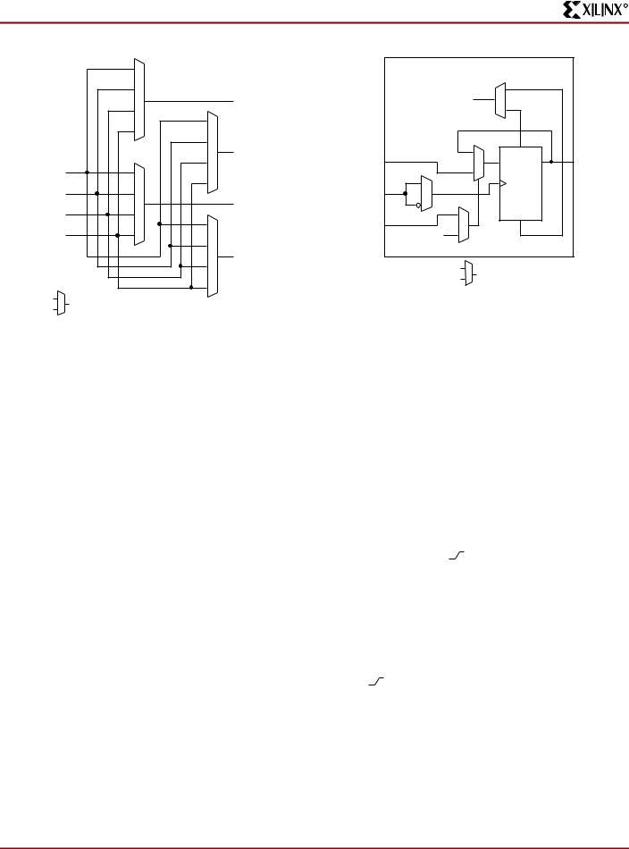
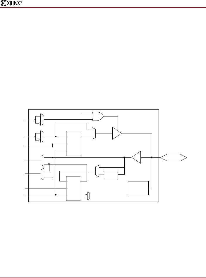
Input/Output Blocks (IOBs)
User-configurable input/output blocks (IOBs) provide the interface between external package pins and the internal logic. Each IOB controls one package pin and can be configured for input, output, or bidirectional signals. Figure 6 shows a simplified functional block diagram of the Spartan/XL IOB.
|
GSR |
|
|
|
|
SD |
|
D |
D |
Q |
Q |
CK |
|
|
|
|
|
RD |
|
EC |
|
|
|
|
Vcc |
|
|
Multiplexer Controlled
by Configuration Program
DS060_05_041901
Figure 5: IOB Flip-Flop/Latch Functional Block
Diagram
IOB Input Signal Path
The input signal to the IOB can be configured to either go directly to the routing channels (via I1 and I2 in Figure 6) or to the input register. The input register can be programmed as either an edge-triggered flip-flop or a level-sensitive latch. The functionality of this register is shown in Table 3, and a simplified block diagram of the register can be seen in Figure 5.
Table 3: Input Register Functionality
Mode |
|
CK |
|
EC |
D |
Q |
||
Power-Up or |
|
X |
|
X |
X |
SR |
||
GSR |
|
|
|
|
|
|
|
|
|
|
|
|
|
|
|
|
|
Flip-Flop |
|
|
|
|
1* |
D |
D |
|
|
|
|
|
|||||
|
|
|
|
|
|
|
|
|
|
|
0 |
|
|
X |
X |
Q |
|
|
|
|
|
|
|
|
|
|
Latch |
1 |
|
|
1* |
X |
Q |
||
|
|
|
|
|
|
|
|
|
|
|
0 |
|
|
1* |
D |
D |
|
|
|
|
|
|
|
|
|
|
Both |
|
X |
|
0 |
X |
Q |
||
|
|
|
|
|
|
|
|
|
Legend: |
|
|
|
|
|
|
|
|
X |
Don’t care. |
|
|
|
||||
|
|
Rising edge (clock not inverted). |
||||||
SR |
Set or Reset value. Reset is default. |
|||||||
0* |
|
Input is Low or unconnected (default |
||||||
|
|
value) |
|
|
|
|||
1* |
|
Input is High or unconnected (default |
||||||
|
|
value) |
|
|
|
|||
6 |
www.xilinx.com |
DS060 (v1.6) September 19, 2001 |
|
1-800-255-7778 |
Product Specification |
R
Spartan and Spartan-XL Families Field Programmable Gate Arrays
The register choice is made by placing the appropriate library symbol. For example, IFD is the basic input flip-flop (rising edge triggered), and ILD is the basic input latch (transparent-High). Variations with inverted clocks are also available. The clock signal inverter is also shown in Figure 5 on the CK line.
The Spartan IOB data input path has a one-tap delay element: either the delay is inserted (default), or it is not. The Spartan-XL IOB data input path has a two-tap delay element, with choices of a full delay, a partial delay, or no delay. The added delay guarantees a zero hold time with respect to clocks routed through the global clock buffers. (See Global Nets and Buffers, page 12 for a description of the global clock buffers in the Spartan/XL families.) For a shorter input register setup time, with positive hold-time, attach a NODELAY attribute or property to the flip-flop.The output of the input register goes to the routing channels (via I1 and I2 in Figure 6). The I1 and I2 signals that exit the IOB can each carry either the direct or registered input signal.
The 5V Spartan input buffers can be globally configured for either TTL (1.2V) or CMOS (VCC/2) thresholds, using an option in the bitstream generation software. The Spartan output levels are also configurable; the two global adjustments of input threshold and output level are independent. The inputs of Spartan devices can be driven by the outputs of any 3.3V device, if the Spartan inputs are in TTL mode. Input and output thresholds are TTL on all configuration pins until the configuration has been loaded into the device and specifies how they are to be used. Spartan-XL inputs are TTL compatible and 3.3V CMOS compatible.
Supported sources for Spartan/XL device inputs are shown in Table 4.
Spartan-XL I/Os are fully 5V tolerant even though the VCC is 3.3V. This allows 5V signals to directly connect to the Spar- tan-XL inputs without damage, as shown in Table 4. In addition, the 3.3V VCC can be applied before or after 5V signals are applied to the I/Os. This makes the Spartan-XL devices immune to power supply sequencing problems.
|
|
GTS |
|
T |
|
|
|
O |
D |
Q |
|
|
CK |
OUTPUT DRIVER |
|
OK |
Programmable Slew Rate |
||
EC |
Programmable TTL/CMOS Drive |
||
|
(Spartan only) |
||
|
|
|
Package |
I1 |
|
|
Pad |
|
|
|
|
|
|
|
INPUT BUFFER |
I2 |
|
Delay |
|
|
|
|
|
|
D |
Q |
Programmable |
|
|
|
|
IK |
CK |
|
Pull-Up/ |
|
Pull-Down |
||
|
|
|
|
EC |
EC |
Multiplexer Controlled |
Network |
|
|||
|
|
by Configuration Program |
|
|
|
|
DS060_06_041901 |
Figure 6: Simplified Spartan/XL IOB Block Diagram
DS060 (v1.6) September 19, 2001 |
www.xilinx.com |
7 |
Product Specification |
1-800-255-7778 |
|
Spartan and Spartan-XL Families Field Programmable Gate Arrays
R
Table 4: Supported Sources for Spartan/XL Inputs
|
|
Spartan |
Spartan-XL |
||
|
|
Inputs |
Inputs |
||
|
|
|
|
|
|
|
|
5V, |
5V, |
3.3V |
|
|
|
|
|||
Source |
TTL |
CMOS |
CMOS |
||
|
|
|
|
|
|
Any device, VCC = 3.3V, |
√ |
Unreli- |
√ |
||
CMOS outputs |
|
able |
|
||
|
|
|
Data |
|
|
Spartan family, VCC = 5V, |
√ |
|
√ |
||
|
|
||||
TTL outputs |
|
|
|
|
|
|
|
|
|
|
|
Any device, VCC = 5V, |
√ |
|
|
√ |
|
TTL outputs (VOH ≤ 3.7V) |
|
|
|
|
|
Any device, VCC = 5V, |
√ |
√ |
√ (default |
||
CMOS outputs |
|
|
|
mode) |
|
|
|
|
|
|
|
Spartan-XL VCC Clamping
Spartan-XL FPGAs have an optional clamping diode connected from each I/O to VCC. When enabled they clamp ringing transients back to the 3.3V supply rail. This clamping action is required in 3.3V PCI applications. VCC clamping is a global option affecting all I/O pins.
Spartan-XL devices are fully 5V TTL I/O compatible if VCC clamping is not enabled. With VCC clamping enabled, the Spartan-XL devices will begin to clamp input voltages to one diode voltage drop above VCC. If enabled, TTL I/O compatibility is maintained but full 5V I/O tolerance is sacrificed. The user may select either 5V tolerance (default) or 3.3V PCI compatibility. In both cases negative voltage is clamped to one diode voltage drop below ground.
Spartan-XL devices are compatible with TTL, LVTTL, PCI 3V, PCI 5V and LVCMOS signalling. The various standards are illustrated in Table 5.
Table 5: I/O Standards Supported by Spartan-XL FPGAs
Signaling |
VCC |
Output |
|
|
|
|
|
Standard |
Clamping |
Drive |
VIH MAX |
VIH MIN |
VIL MAX |
VOH MIN |
VOL MAX |
TTL |
Not allowed |
12/24 mA |
5.5 |
2.0 |
0.8 |
2.4 |
0.4 |
|
|
|
|
|
|
|
|
LVTTL |
OK |
12/24 mA |
3.6 |
2.0 |
0.8 |
2.4 |
0.4 |
|
|
|
|
|
|
|
|
PCI5V |
Not allowed |
24 mA |
5.5 |
2.0 |
0.8 |
2.4 |
0.4 |
|
|
|
|
|
|
|
|
PCI3V |
Required |
12 mA |
3.6 |
50% of VCC |
30% of VCC |
90% of VCC |
10% of VCC |
LVCMOS 3V |
OK |
12/24 mA |
3.6 |
50% of VCC |
30% of VCC |
90% of VCC |
10% of VCC |
Additional Fast Capture Input Latch (Spartan-XL only)
The Spartan-XL IOB has an additional optional latch on the input. This latch is clocked by the clock used for the output flip-flop rather than the input clock. Therefore, two different clocks can be used to clock the two input storage elements. This additional latch allows the fast capture of input data, which is then synchronized to the internal clock by the IOB flip-flop or latch.
To place the Fast Capture latch in a design, use one of the special library symbols, ILFFX or ILFLX. ILFFX is a trans- parent-Low Fast Capture latch followed by an active High input flip-flop. ILFLX is a transparent Low Fast Capture latch followed by a transparent High input latch. Any of the clock inputs can be inverted before driving the library element, and the inverter is absorbed into the IOB.
IOB Output Signal Path
Output signals can be optionally inverted within the IOB, and can pass directly to the output buffer or be stored in an edge-triggered flip-flop and then to the output buffer. The functionality of this flip-flop is shown in Table 6.
Table 6: Output Flip-Flop Functionality |
|
|
|||
|
|
Clock |
|
|
|
Mode |
Clock |
Enable |
T |
D |
Q |
Power-Up |
X |
X |
0* |
X |
SR |
or GSR |
|
|
|
|
|
Flip-Flop |
X |
0 |
0* |
X |
Q |
|
|
1* |
0* |
D |
D |
|
X |
X |
1 |
X |
Z |
|
0 |
X |
0* |
X |
Q |
Legend: |
|
|
|
|
|
X Don’t care
Rising edge (clock not inverted). SR Set or Reset value. Reset is default.
0* Input is Low or unconnected (default value)
1* Input is High or unconnected (default value) Z 3-state
8 |
www.xilinx.com |
DS060 (v1.6) September 19, 2001 |
|
1-800-255-7778 |
Product Specification |

R
Spartan and Spartan-XL Families Field Programmable Gate Arrays
Output Multiplexer/2-Input Function Generator (Spartan-XL only)
The output path in the Spartan-XL IOB contains an additional multiplexer not available in the Spartan IOB. The multiplexer can also be configured as a 2-input function generator, implementing a pass gate, AND gate, OR gate, or XOR gate, with 0, 1, or 2 inverted inputs.
When configured as a multiplexer, this feature allows two output signals to time-share the same output pad, effectively doubling the number of device outputs without requiring a larger, more expensive package. The select input is the pin used for the output flip-flop clock, OK.
When the multiplexer is configured as a 2-input function generator, logic can be implemented within the IOB itself. Combined with a Global buffer, this arrangement allows very high-speed gating of a single signal. For example, a wide decoder can be implemented in CLBs, and its output gated with a Read or Write Strobe driven by a global buffer.
The user can specify that the IOB function generator be used by placing special library symbols beginning with the letter "O." For example, a 2-input AND gate in the IOB function generator is called OAND2. Use the symbol input pin labeled "F" for the signal on the critical path. This signal is placed on the OK pin — the IOB input with the shortest delay to the function generator. Two examples are shown in Figure 7.
OMUX2
F |
|
|
D0 |
|
||
|
|
|
|
|
O |
|
|
|
|
|
|
|
|
OAND2 |
|
D1 |
|
|||
|
|
|
|
|
|
|
|
S0 |
|
|
|||
|
|
|||||
|
|
|
|
|
|
|
DS060_07_081100
Figure 7: AND and MUX Symbols in Spartan-XL IOB
Output Buffer
An active High 3-state signal can be used to place the output buffer in a high-impedance state, implementing 3-state outputs or bidirectional I/O. Under configuration control, the output (O) and output 3-state (T) signals can be inverted. The polarity of these signals is independently configured for each IOB (see Figure 6, page 7). An output can be configured as open-drain (open-collector) by tying the 3-state pin
(T) to the output signal, and the input pin (I) to Ground.
By default, a 5V Spartan device output buffer pull-up structure is configured as a TTL-like totem-pole. The High driver is an n-channel pull-up transistor, pulling to a voltage one transistor threshold below VCC. Alternatively, the outputs can be globally configured as CMOS drivers, with additional p-channel pull-up transistors pulling to VCC. This option, applied using the bitstream generation software, applies to all outputs on the device. It is not individually programmable.
All Spartan-XL device outputs are configured as CMOS drivers, therefore driving rail-to-rail. The Spartan-XL outputs are individually programmable for 12 mA or 24 mA output drive.
Any 5V Spartan device with its outputs configured in TTL mode can drive the inputs of any typical 3.3V device. Supported destinations for Spartan/XL device outputs are shown in Table 7.
Three-State Register (Spartan-XL Only)
Spartan-XL devices incorporate an optional register controlling the three-state enable in the IOBs. The use of the three-state control register can significantly improve output enable and disable time.
Output Slew Rate
The slew rate of each output buffer is, by default, reduced, to minimize power bus transients when switching non-criti- cal signals. For critical signals, attach a FAST attribute or property to the output buffer or flip-flop.
Spartan/XL devices have a feature called "Soft Start-up," designed to reduce ground bounce when all outputs are turned on simultaneously at the end of configuration. When the configuration process is finished and the device starts up, the first activation of the outputs is automatically slew-rate limited. Immediately following the initial activation of the I/O, the slew rate of the individual outputs is determined by the individual configuration option for each IOB.
Pull-up and Pull-down Network
Programmable pull-up and pull-down resistors are used for tying unused pins to VCC or Ground to minimize power consumption and reduce noise sensitivity. The configurable pull-up resistor is a p-channel transistor that pulls to VCC. The configurable pull-down resistor is an n-channel transistor that pulls to Ground. The value of these resistors is typically 20 KΩ − 100 KΩ (See "Spartan DC Characteristics
DS060 (v1.6) September 19, 2001 |
www.xilinx.com |
9 |
Product Specification |
1-800-255-7778 |
|

Spartan and Spartan-XL Families Field Programmable Gate Arrays
R
Over Operating Conditions" on page 43.). This high value makes them unsuitable as wired-AND pull-up resistors.
Table 7: Supported Destinations for Spartan/XL
Outputs
|
Spartan-XL |
|
Spartan |
|
|
Outputs |
|
Outputs |
|
|
|
|
|
|
|
|
|
5V, |
5V, |
Destination |
3.3V, CMOS |
|
TTL |
CMOS |
|
|
|
|
|
Any device, |
√ |
|
√ |
Some(1) |
VCC = 3.3V, |
|
|
|
|
CMOS-threshold |
|
|
|
|
inputs |
|
|
|
|
|
|
|
|
|
Any device, |
√ |
|
√ |
√ |
VCC = 5V, |
|
|
|
|
TTL-threshold inputs |
|
|
|
|
|
|
|
|
|
Any device, |
Unreliable |
|
√ |
|
VCC = 5V, |
Data |
|
|
|
CMOS-threshold |
|
|
|
|
inputs |
|
|
|
|
|
|
|
|
|
Notes:
1.Only if destination device has 5V tolerant inputs.
After configuration, voltage levels of unused pads, bonded or unbonded, must be valid logic levels, to reduce noise sensitivity and avoid excess current. Therefore, by default, unused pads are configured with the internal pull-up resistor active. Alternatively, they can be individually configured with the pull-down resistor, or as a driven output, or to be driven by an external source. To activate the internal pull-up, attach the PULLUP library component to the net attached to the pad. To activate the internal pull-down, attach the PULLDOWN library component to the net attached to the pad.
Set/Reset
As with the CLB registers, the GSR signal can be used to set or clear the input and output registers, depending on the value of the INIT attribute or property. The two flip-flops can be individually configured to set or clear on reset and after configuration. Other than the global GSR net, no user-con- trolled set/reset signal is available to the I/O flip-flops (Figure 5). The choice of set or reset applies to both the initial state of the flip-flop and the response to the GSR pulse.
Independent Clocks
Separate clock signals are provided for the input (IK) and output (OK) flip-flops. The clock can be independently inverted for each flip-flop within the IOB, generating either
falling-edge or rising-edge triggered flip-flops. The clock inputs for each IOB are independent.
Common Clock Enables
The input and output flip-flops in each IOB have a common clock enable input (see EC signal in Figure 5), which through configuration, can be activated individually for the input or output flip-flop, or both. This clock enable operates exactly like the EC signal on the Spartan/XL CLB. It cannot be inverted within the IOB.
Routing Channel Description
All internal routing channels are composed of metal segments with programmable switching points and switching matrices to implement the desired routing. A structured, hierarchical matrix of routing channels is provided to achieve efficient automated routing.
This section describes the routing channels available in Spartan/XL devices. Figure 8 shows a general block diagram of the CLB routing channels. The implementation software automatically assigns the appropriate resources based on the density and timing requirements of the design. The following description of the routing channels is for information only and is simplified with some minor details omitted. For an exact interconnect description the designer should open a design in the FPGA Editor and review the actual connections in this tool.
The routing channels will be discussed as follows;
•CLB routing channels which run along each row and column of the CLB array.
•IOB routing channels which form a ring (called a VersaRing) around the outside of the CLB array. It connects the I/O with the CLB routing channels.
•Global routing consists of dedicated networks primarily designed to distribute clocks throughout the device with minimum delay and skew. Global routing can also be used for other high-fanout signals.
CLB Routing Channels
The routing channels around the CLB are derived from three types of interconnects; single-length, double-length, and longlines. At the intersection of each vertical and horizontal routing channel is a signal steering matrix called a Programmable Switch Matrix (PSM). Figure 8 shows the basic routing channel configuration showing single-length lines, double-length lines and longlines as well as the CLBs and PSMs. The CLB to routing channel interface is shown as well as how the PSMs interface at the channel intersections.
10 |
www.xilinx.com |
DS060 (v1.6) September 19, 2001 |
|
1-800-255-7778 |
Product Specification |

R
Spartan and Spartan-XL Families Field Programmable Gate Arrays
PSM |
PSM |
PSM 8 Singles |
|
|
|
2 |
Doubles |
|
|
3 |
Longs |
|
CLB |
CLB |
|
|
|
3 |
Longs |
|
|
2 |
Doubles |
PSM |
PSM |
PSM |
|
2 Doubles |
3 Longs 8 Singles 3 Longs |
2 Doubles |
|
|
|
DS060_09_041901 |
|
Figure 8: Spartan/XL CLB Routing Channels and Interface Block Diagram
CLB Interface
A block diagram of the CLB interface signals is shown in Figure 9. The input signals to the CLB are distributed evenly on all four sides providing maximum routing flexibility. In general, the entire architecture is symmetrical and regular. It is well suited to established placement and routing algorithms. Inputs, outputs, and function generators can freely swap positions within a CLB to avoid routing congestion during the placement and routing operation. The exceptions are the clock (K) input and CIN/COUT signals. The K input is routed to dedicated global vertical lines as well as four single-length lines and is on the left side of the CLB. The CIN/COUT signals are routed through dedicated interconnects which do not interfere with the general routing structure. The output signals from the CLB are available to drive both vertical and horizontal channels.
|
|
|
|
|
|
F4 |
|
C4 |
G4 |
YQ |
||||||||
CIN |
|
|
|
|
|
|
|
|
|
|
|
|
|
|
|
|
Y |
|
|
|
|
|
|
|
|
|
|
|
|
|
|
|
|
|
|
||
|
|
|
|
|
|
|
|
|
|
|
|
|
|
|
|
|
||
|
|
|
|
|
|
|
|
|
|
|
|
|
|
|
|
|
||
|
|
|
|
|
|
|
|
|
|
|
|
|
|
|
|
|
||
|
|
|
|
|
|
|
|
|
|
|
|
|
|
|
||||
COUT |
|
|
|
|
|
|
|
|
|
|
|
|
|
|
|
G3 |
||
|
|
|
|
|
|
|
|
|
|
|
|
|
|
|
||||
G1 |
|
|
|
|
|
|
CLB |
|
|
|
|
|
|
|
C3 |
|||
|
|
|
|
|
|
|
|
|
|
|
|
|||||||
C1 |
|
|
|
|
|
|
|
|
|
|
|
|
|
|
||||
|
|
|
|
|
|
|
|
|
|
|
|
|
|
|||||
|
|
|
|
|
|
|
|
|
|
|
|
|
|
|
||||
|
|
|
|
|
|
|
|
|
|
|
|
|
|
|
|
|
||
K |
|
|
|
|
|
|
|
|
|
|
|
|
|
|
|
|
F3 |
|
|
|
|
|
|
|
|
|
|
|
|
|
|
|
|
||||
F1 |
|
|
|
|
|
|
|
|
|
|
|
|
|
|
|
|
|
|
|
|
|
|
|
|
|
|
|
|
|
|
|
|
|
|
|
||
|
|
|
|
|
|
|
|
|
|
|
|
|
|
|
|
|
||
|
|
|
|
|
|
|
|
|
|
|
|
|
|
|
|
|||
X |
|
|
|
|
|
|
|
|
Rev 1.1 |
|
|
|
|
|||||
|
|
|
|
|
|
|
|
|
|
|
|
|||||||
|
|
|
|
|
|
|
|
|
|
|
|
|
|
|
||||
|
|
|
|
|
|
|
|
|
|
|
|
|
|
|
|
|
|
|
|
|
|
|
|
|
|
|
|
|
|
|
|
|
|
|
|
|
|
|
|
|
|
|
|
|
|
|
|
|
|
|
|
|
|
|
|
|
|
|
|
|
|
|
|
|
|
|
|
|
|
|
|
|
|
|
|
Programmable Switch Matrices
The horizontal and vertical singleand double-length lines intersect at a box called a programmable switch matrix (PSM). Each PSM consists of programmable pass transistors used to establish connections between the lines (see Figure 10).
For example, a single-length signal entering on the right side of the switch matrix can be routed to a single-length line on the top, left, or bottom sides, or any combination thereof, if multiple branches are required. Similarly, a dou- ble-length signal can be routed to a double-length line on any or all of the other three edges of the programmable switch matrix.
Single-Length Lines
Single-length lines provide the greatest interconnect flexibility and offer fast routing between adjacent blocks. There are eight vertical and eight horizontal single-length lines associated with each CLB. These lines connect the switching matrices that are located in every row and column of CLBs. Single-length lines are connected by way of the programmable switch matrices, as shown in Figure 10. Routing connectivity is shown in Figure 8.
Single-length lines incur a delay whenever they go through a PSM. Therefore, they are not suitable for routing signals for long distances. They are normally used to conduct signals within a localized area and to provide the branching for nets with fanout greater than one.
XQ |
F2 |
C2 |
G2 |
|
|
|
|
DS060_08_081100 |
|
Figure 9: CLB Interconnect Signals |
|
|||
|
|
|
||
DS060 (v1.6) September 19, 2001 |
www.xilinx.com |
11 |
||
Product Specification |
|
|
1-800-255-7778 |
|
Spartan and Spartan-XL Families Field Programmable Gate Arrays
R
Six Pass Transistors Per
Switch Matrix Interconnect Point
DS060_10_081100
Figure 10: Programmable Switch Matrix
Double-Length Lines |
I/O Routing |
The double-length lines consist of a grid of metal segments, each twice as long as the single-length lines: they run past two CLBs before entering a PSM. Double-length lines are grouped in pairs with the PSMs staggered, so that each line goes through a PSM at every other row or column of CLBs (see Figure 8).
There are four vertical and four horizontal double-length lines associated with each CLB. These lines provide faster signal routing over intermediate distances, while retaining routing flexibility.
Longlines
Longlines form a grid of metal interconnect segments that run the entire length or width of the array. Longlines are intended for high fan-out, time-critical signal nets, or nets that are distributed over long distances.
Each Spartan/XL device longline has a programmable splitter switch at its center. This switch can separate the line into two independent routing channels, each running half the width or height of the array.
Routing connectivity of the longlines is shown in Figure 8. The longlines also interface to some 3-state buffers which is described later in 3-State Long Line Drivers, page 19.
Spartan/XL devices have additional routing around the IOB ring. This routing is called a VersaRing. The VersaRing facilitates pin-swapping and redesign without affecting board layout. Included are eight double-length lines, and four longlines.
Global Nets and Buffers
The Spartan/XL devices have dedicated global networks. These networks are designed to distribute clocks and other high fanout control signals throughout the devices with minimal skew.
Four vertical longlines in each CLB column are driven exclusively by special global buffers. These longlines are in addition to the vertical longlines used for standard interconnect. In the 5V Spartan devices, the four global lines can be driven by either of two types of global buffers; Primary Global buffers (BUFGP) or Secondary Global buffers (BUFGS). Each of these lines can be accessed by one particular Primary Global buffer, or by any of the Secondary Global buffers, as shown in Figure 11. In the 3V Spartan-XL devices, the four global lines can be driven by any of the eight Global Low-Skew Buffers (BUFGLS). The clock pins of every CLB and IOB can also be sourced from local interconnect.
12 |
www.xilinx.com |
DS060 (v1.6) September 19, 2001 |
|
1-800-255-7778 |
Product Specification |
R
Spartan and Spartan-XL Families Field Programmable Gate Arrays
BUFGS
PGCK1
SGCK1
BUFGP 
4
IOB
locals
 X4
X4
locals
IOB
BUFGS
PGCK2
SGCK2
BUFGP
IOB
locals
Any BUFGS
One BUFGP per Global Line
locals
IOB
|
IOB |
|
IOB |
IOB |
locals |
|
|
locals |
locals |
|
4 |
|
4 |
|
|
|
|
|
|
locals |
|
|
locals |
|
|
CLB |
CLB |
|
|
X4 |
|
|
X4 |
|
locals |
CLB |
CLB |
locals |
|
|
|
|
||
locals |
|
|
locals |
locals |
|
IOB |
|
IOB |
IOB |
Any BUFGS
One BUFGP per Global Line
BUFGP
SGCK4
PGCK4
BUFGS
4
IOB
locals
X4 
locals
IOB
 BUFGP
BUFGP
SGCK3
PGCK3
BUFGS
ds060_11_080400
Figure 11: 5V Spartan Family Global Net Distribution
The four Primary Global buffers offer the shortest delay and negligible skew. Four Secondary Global buffers have slightly longer delay and slightly more skew due to potentially heavier loading, but offer greater flexibility when used to drive non-clock CLB inputs. The eight Global Low-Skew buffers in the Spartan-XL devices combine short delay, negligible skew, and flexibility.
The Primary Global buffers must be driven by the semi-ded- icated pads (PGCK1-4). The Secondary Global buffers can be sourced by either semi-dedicated pads (SGCK1-4) or internal nets. Each corner of the device has one Primary buffer and one Secondary buffer. The Spartan-XL family has eight global low-skew buffers, two in each corner. All can be sourced by either semi-dedicated pads (GCK1-8) or internal nets.
Using the library symbol called BUFG results in the software choosing the appropriate clock buffer, based on the timing requirements of the design. A global buffer should be specified for all timing-sensitive global signal distribution. To use a global buffer, place a BUFGP (primary buffer), BUFGS (secondary buffer), BUFGLS (Spartan-XL global low-skew buffer), or BUFG (any buffer type) element in a schematic or in HDL code.
Advanced Features Description
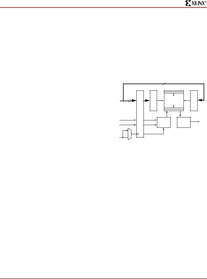
Distributed RAM
Optional modes for each CLB allow the function generators (F-LUT and G-LUT) to be used as Random Access Memory (RAM).
Read and write operations are significantly faster for this on-chip RAM than for off-chip implementations. This speed advantage is due to the relatively short signal propagation delays within the FPGA.
Memory Configuration Overview
There are two available memory configuration modes: sin- gle-port RAM and dual-port RAM. For both these modes, write operations are synchronous (edge-triggered), while read operations are asynchronous. In the single-port mode, a single CLB can be configured as either a 16 x 1, (16 x 1) x 2, or 32 x 1 RAM array. In the dual-port mode, a single CLB can be configured only as one 16 x 1 RAM array. The different CLB memory configurations are summarized in Table 8. Any of these possibilities can be individually programmed into a Spartan/XL CLB.
|
|
Table 8: CLB Memory Configurations |
|
|
||
|
|
Mode |
16 x 1 |
(16 x 1) x 2 |
32 x 1 |
|
|
|
|
|
|
|
|
|
|
Single-Port |
√ |
√ |
√ |
|
|
|
|
|
|
|
|
|
|
Dual-Port |
√ |
− |
− |
|
|
|
|
|
|
|
|
|
|
|
|
|
|
|
DS060 (v1.6) September 19, 2001 |
www.xilinx.com |
|
|
13 |
||
Product Specification |
1-800-255-7778 |
|
|
|
|
|
Spartan and Spartan-XL Families Field Programmable Gate Arrays
R
•The 16 x 1 single-port configuration contains a RAM array with 16 locations, each one-bit wide. One 4-bit address decoder determines the RAM location for write and read operations. There is one input for writing data and one output for reading data, all at the selected address.
•The (16 x 1) x 2 single-port configuration combines two 16 x 1 single-port configurations (each according to the preceding description). There is one data input, one data output and one address decoder for each array. These arrays can be addressed independently.
•The 32 x 1 single-port configuration contains a RAM array with 32 locations, each one-bit wide. There is one data input, one data output, and one 5-bit address decoder.
•The dual-port mode 16 x 1 configuration contains a RAM array with 16 locations, each one-bit wide. There are two 4-bit address decoders, one for each port. One port consists of an input for writing and an output for reading, all at a selected address. The other port consists of one output for reading from an independently selected address.
The appropriate choice of RAM configuration mode for a given design should be based on timing and resource requirements, desired functionality, and the simplicity of the design process. Selection criteria include the following: Whereas the 32 x 1 single-port, the (16 x 1) x 2 single-port, and the 16 x 1 dual-port configurations each use one entire CLB, the 16 x 1 single-port configuration uses only one half of a CLB. Due to its simultaneous read/write capability, the dual-port RAM can transfer twice as much data as the sin- gle-port RAM, which permits only one data operation at any given time.
CLB memory configuration options are selected by using the appropriate library symbol in the design entry.
Single-Port Mode
There are three CLB memory configurations for the sin- gle-port RAM: 16 x 1, (16 x 1) x 2, and 32 x 1, the functional organization of which is shown in Figure 12.
The single-port RAM signals and the CLB signals (Figure 2, page 4) from which they are originally derived are shown in Table 9.
Table 9: Single-Port RAM Signals
RAM Signal |
Function |
CLB Signal |
|
|
|
D0 or D1 |
Data In |
DIN or H1 |
|
|
|
A[3:0] |
Address |
F[4:1] or G[4:1] |
|
|
|
A4 (32 x 1 only) |
Address |
H1 |
|
|
|
WE |
Write Enable |
SR |
|
|
|
WCLK |
Clock |
K |
|
|
|
SPO |
Single Port Out |
FOUT or GOUT |
|
(Data Out) |
|
|
|
|
|
|
|
|
n |
|
|
|
|
REGISTER |
WRITEROW |
SELECT |
|
16 x 1 |
READ ROW |
SELECT |
A[n-1:0] |
n |
|
|
|
32 x 1 |
|
|
|
|
|
|
RAM ARRAY |
|
|
|
WE |
INPUT |
|
|
CONTROL |
OUT |
|
|
|
|
|
|
WRITE |
READ |
|
SPO |
|
|
|
|
|
|
|
|
D0 or D1 |
|
|
|
|
|
|
|
WCLK |
|
|
|
|
|
DS060_12_043010 |
|
|
|
|
|
|
|
||
Notes:
1.The (16 x 1) x 2 configuration combines two 16 x 1 single-port RAMs, each with its own independent address bus and data input. The same WE and WCLK signals are connected to both RAMs.
2.n = 4 for the 16 x 1 and (16 x 1) x 2 configurations. n = 5 for the 32 x 1 configuration.
Figure 12: Logic Diagram for the Single-Port RAM
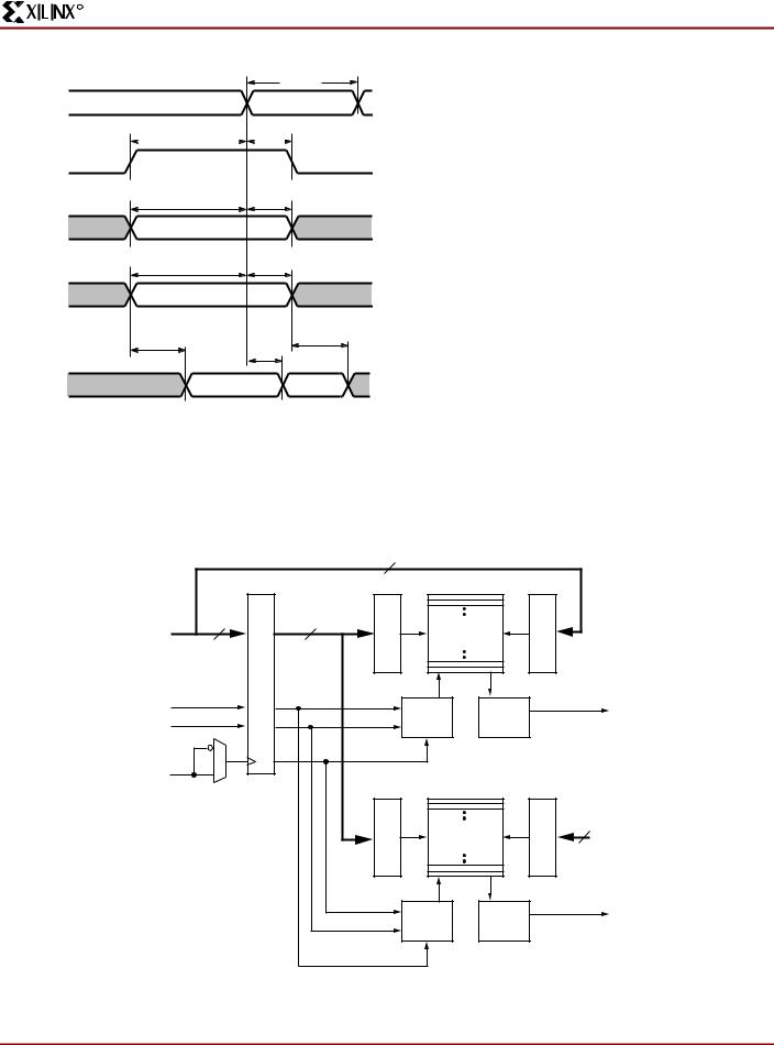
Writing data to the single-port RAM is essentially the same as writing to a data register. It is an edge-triggered (synchronous) operation performed by applying an address to the A inputs and data to the D input during the active edge of WCLK while WE is High.
The timing relationships are shown in Figure 13. The High logic level on WE enables the input data register for writing. The active edge of WCLK latches the address, input data, and WE signals. Then, an internal write pulse is generated that loads the data into the memory cell.
14 |
www.xilinx.com |
DS060 (v1.6) September 19, 2001 |
|
1-800-255-7778 |
Product Specification |
R
Spartan and Spartan-XL Families Field Programmable Gate Arrays
TWPS
WCLK (K)
TWSS |
|
TWHS |
WE
TDSS TDHS
DATA IN
TASS TAHS
ADDRESS
TILO |
TWOS |
TILO |
|
|
|
DATA OUT |
OLD |
NEW |
DS060_13_080400
Figure 13: Data Write and Access Timing for RAM
WCLK can be configured as active on either the rising edge (default) or the falling edge. While the WCLK input to the RAM accepts the same signal as the clock input to the associated CLB’s flip-flops, the sense of this WCLK input can be
inverted with respect to the sense of the flip-flop clock inputs. Consequently, within the same CLB, data at the RAMs SPO line can be stored in a flip-flop with either the same or the inverse clock polarity used to write data to the RAM.
The WE input is active High and cannot be inverted within the CLB.
Allowing for settling time, the data on the SPO output reflects the contents of the RAM location currently addressed. When the address changes, following the asynchronous delay TILO, the data stored at the new address location will appear on SPO. If the data at a particular RAM address is overwritten, after the delay TWOS, the new data will appear on SPO.
Dual-Port Mode
In dual-port mode, the function generators (F-LUT and G-LUT) are used to create a 16 x 1 dual-port memory. Of the two data ports available, one permits read and write operations at the address specified by A[3:0] while the second provides only for read operations at the address specified independently by DPRA[3:0]. As a result, simultaneous read/write operations at different addresses (or even at the same address) are supported.
The functional organization of the 16 x 1 dual-port RAM is shown in Figure 14. The dual-port RAM signals and the
|
|
4 |
|
|
|
|
|
A[3:0] |
4 |
4 |
|
16 x 1 |
|
|
|
|
WRITEROW |
SELECT |
RAM |
READROW |
SELECT |
|
|
|
REGISTER |
|
|||||
|
|
|
|||||
WE |
INPUT |
|
WRITE |
|
READ |
|
SPO |
|
|
|
|
||||
D |
|
CONTROL |
|
OUT |
|
|
|
|
|
|
|
|
|||
|
|
|
|
|
|
|
|
WCLK |
|
|
|
|
|
|
|
|
|
WRITE ROW |
SELECT |
16 x 1 |
READ ROW |
SELECT |
4 |
|
|
RAM |
DPRA[3:0] |
||||
|
|
|
|||||
|
|
|
|
||||
|
|
|
WRITE |
|
READ |
|
DPO |
|
|
|
CONTROL |
|
OUT |
|
|
|
|
|
|
|
|
|
DS060_14_043001 |
Figure 14: Logic Diagram for the Dual-Port RAM
DS060 (v1.6) September 19, 2001 |
www.xilinx.com |
15 |
Product Specification |
1-800-255-7778 |
|
Spartan and Spartan-XL Families Field Programmable Gate Arrays
R
CLB signals from which they are originally derived are shown in Table 10.
Table 10: Dual-Port RAM Signals
RAM Signal |
Function |
CLB Signal |
|
|
|
D |
Data In |
DIN |
|
|
|
A[3:0] |
Read Address for |
F[4:1] |
|
Single-Port. |
|
|
Write Address for |
|
|
Single-Port and |
|
|
Dual-Port. |
|
|
|
|
DPRA[3:0] |
Read Address for |
G[4:1] |
|
Dual-Port |
|
|
|
|
WE |
Write Enable |
SR |
|
|
|
WCLK |
Clock |
K |
|
|
|
SPO |
Single Port Out |
FOUT |
|
(addressed by A[3:0]) |
|
|
|
|
DPO |
Dual Port Out |
GOUT |
|
(addressed by |
|
|
DPRA[3:0]) |
|
|
|
|
The RAM16X1D primitive used to instantiate the dual-port RAM consists of an upper and a lower 16 x 1 memory array. The address port labeled A[3:0] supplies both the read and write addresses for the lower memory array, which behaves the same as the 16 x 1 single-port RAM array described previously. Single Port Out (SPO) serves as the data output for the lower memory. Therefore, SPO reflects the data at address A[3:0].
The other address port, labeled DPRA[3:0] for Dual Port Read Address, supplies the read address for the upper memory. The write address for this memory, however, comes from the address A[3:0]. Dual Port Out (DPO) serves as the data output for the upper memory. Therefore, DPO reflects the data at address DPRA[3:0].
By using A[3:0] for the write address and DPRA[3:0] for the read address, and reading only the DPO output, a FIFO that can read and write simultaneously is easily generated. The simultaneous read/write capability possible with the dual-port RAM can provide twice the effective data throughput of a single-port RAM alternating read and write operations.
The timing relationships for the dual-port RAM mode are shown in Figure 13.
attached to the RAM or ROM symbol, as described in the schematic library guide. If not defined, all RAM contents are initialized to zeros, by default.
RAM initialization occurs only during device configuration. The RAM content is not affected by GSR.
More Information on Using RAM Inside CLBs
Three application notes are available from Xilinx that discuss synchronous (edge-triggered) RAM: "Xilinx Edge-Trig- gered and Dual-Port RAM Capability," "Implementing FIFOs in Xilinx RAM," and "Synchronous and Asynchronous FIFO Designs." All three application notes apply to both the Spartan and the Spartan-XL families.
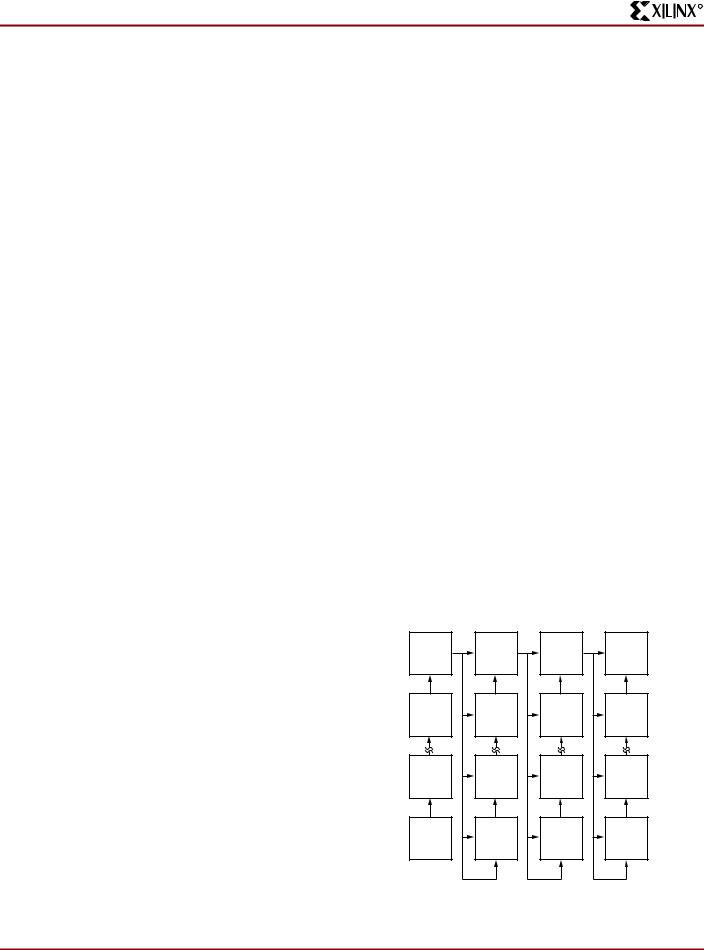
Fast Carry Logic
Each CLB F-LUT and G-LUT contains dedicated arithmetic logic for the fast generation of carry and borrow signals. This extra output is passed on to the function generator in the adjacent CLB. The carry chain is independent of normal routing resources. (See Figure 15.)
Dedicated fast carry logic greatly increases the efficiency and performance of adders, subtractors, accumulators, comparators and counters. It also opens the door to many new applications involving arithmetic operation, where the previous generations of FPGAs were not fast enough or too inefficient. High-speed address offset calculations in microprocessor or graphics systems, and high-speed addition in digital signal processing are two typical applications.
The two 4-input function generators can be configured as a 2-bit adder with built-in hidden carry that can be expanded to any length. This dedicated carry circuitry is so fast and efficient that conventional speed-up methods like carry generate/propagate are meaningless even at the 16-bit level, and of marginal benefit at the 32-bit level. This fast carry logic is one of the more significant features of the Spartan
CLB |
CLB |
CLB |
CLB |
CLB |
CLB |
CLB |
CLB |
CLB |
CLB |
CLB |
CLB |
Note that write operations to RAM are synchronous (edge-triggered); however, data access is asynchronous.
Initializing RAM at FPGA Configuration
Both RAM and ROM implementations in the Spartan/XL families are initialized during device configuration. The initial contents are defined via an INIT attribute or property
CLB |
CLB |
CLB |
CLB |
DS060_15_081100
Figure 15: Available Spartan/XL Carry Propagation
Paths
16 |
www.xilinx.com |
DS060 (v1.6) September 19, 2001 |
|
1-800-255-7778 |
Product Specification |

R
Spartan and Spartan-XL Families Field Programmable Gate Arrays
and Spartan-XL families, speeding up arithmetic and counting functions.
The carry chain in 5V Spartan devices can run either up or down. At the top and bottom of the columns where there are no CLBs above and below, the carry is propagated to the right. The default is always to propagate up the column, as shown in the figures. The carry chain in Spartan-XL devices can only run up the column, providing even higher speed.
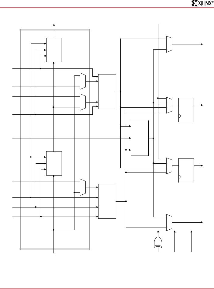
Figure 16, page 18 shows a Spartan/XL CLB with dedicated fast carry logic. The carry logic shares operand and
control inputs with the function generators. The carry outputs connect to the function generators, where they are combined with the operands to form the sums.
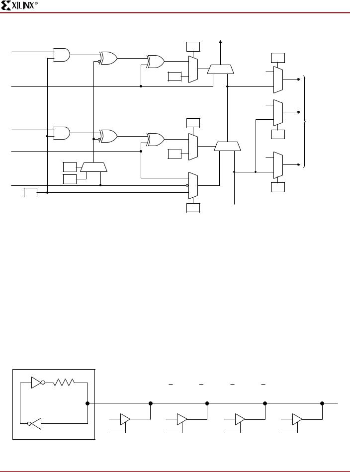
Figure 17, page 19 shows the details of the Spartan/XL carry logic. This diagram shows the contents of the box labeled "CARRY LOGIC" in Figure 16.
The fast carry logic can be accessed by placing special library symbols, or by using Xilinx Relationally Placed Macros (RPMs) that already include these symbols.
DS060 (v1.6) September 19, 2001 |
www.xilinx.com |
17 |
Product Specification |
1-800-255-7778 |
|
Spartan and Spartan-XL Families Field Programmable Gate Arrays
R
COUT |
DIN |
|
|
|
CARRY |
|
|
|
|
LOGIC |
|
|
|
|
|
G |
|
|
|
G |
H |
|
|
Y |
|
|
|
||
CARRY |
|
|
|
|
G4 |
|
|
|
|
G3 |
|
|
|
|
|
G |
|
|
|
G2 |
DIN |
|
|
|
|
|
|
|
|
|
H |
|
S/R |
|
|
G |
D |
Q |
YQ |
|
F |
|
|
|
G1 |
|
|
|
|
|
|
|
EC |
|
COUT0 |
|
|
|
|
H1 |
H |
|
|
|
|
DIN |
|
|
|
F |
H |
|
S/R |
|
CARRY |
G |
D |
Q |
XQ |
|
F |
|
|
|
F4 |
|
|
EC |
|
|
|
|
|
|
F3 |
F |
|
|
|
|
|
|
|
|
F2 |
|
|
|
|
F1 |
H |
|
|
|
|
|
|
|
|
|
F |
|
|
X |
|
|
|
|
|
CIN |
K |
S/R |
EC |
|
|
|
|
|
|
|
|
|
DS060_16_080400 |
|
Figure 16: Fast Carry Logic in Spartan/XL CLB
18 |
www.xilinx.com |
DS060 (v1.6) September 19, 2001 |
|
1-800-255-7778 |
Product Specification |
R
Spartan and Spartan-XL Families Field Programmable Gate Arrays
|
|
|
COUT |
|
|
|
G1 |
|
|
M |
|
|
|
|
|
|
|
|
M |
|
|
|
|
1 |
|
|
|
|
|
|
|
|
|
|
|
|
I |
0 |
1 |
|
G2 |
|
|
0 |
|
|
|
|
G4 |
|
|
|
|
|
|
|
|
|
|
|
|
G3 |
|
|
|
|
|
COUT0 |
TO |
|
|
|
M |
|
|
FUNCTION |
F2 |
|
|
|
|
|
GENERATORS |
|
|
|
1 |
|
|
M |
|
|
|
|
|
|
|
F1 |
|
|
0 |
0 |
1 |
|
|
M |
|
|
F4 |
||
|
|
|
|
|||
|
|
|
|
|
|
|
M |
0 |
1 |
|
|
|
|
M |
|
|
3 |
|
|
|
F3 |
|
|
1 |
|
|
M |
M |
|
|
0 |
|
|
|
|
|
|
|
|
||
|
|
|
M |
|
CIN |
|
|
|
|
|
|
|
DS060_17_080400 |
Figure 17: Detail of Spartan/XL Dedicated Carry Logic
3-State Long Line Drivers
A pair of 3-state buffers is associated with each CLB in the array. These 3-state buffers (BUFT) can be used to drive signals onto the nearest horizontal longlines above and below the CLB. They can therefore be used to implement multiplexed or bidirectional buses on the horizontal longlines, saving logic resources.
There is a weak keeper at each end of these two horizontal longlines. This circuit prevents undefined floating levels. However, it is overridden by any driver.
The buffer enable is an active High 3-state (i.e., an active Low enable), as shown in Table 11.
Three-State Buffer Example
Figure 18 shows how to use the 3-state buffers to implement a multiplexer. The selection is accomplished by the buffer 3-state signal.
Pay particular attention to the polarity of the T pin when using these buffers in a design. Active High 3-state (T) is identical to an active Low output enable, as shown in Table 11.
Table 11: Three-State Buffer Functionality
IN |
T |
OUT |
|
|
|
X |
1 |
Z |
|
|
|
IN |
0 |
IN |
|
|
|
~100 kΩ |
Z = (DA • A) + (DB • B) + (DC • C) + (DN • N) |
|
||
|
|
|
|
|
DA |
DB |
|
DC |
DN |
A |
BUFT |
BUFT |
BUFT |
BUFT |
B |
|
C |
N |
|
"Weak Keeper"
DS060_18_080400
Figure 18: 3-state Buffers Implement a Multiplexer
DS060 (v1.6) September 19, 2001 |
www.xilinx.com |
19 |
Product Specification |
1-800-255-7778 |
|

Spartan and Spartan-XL Families Field Programmable Gate Arrays
R
On-Chip Oscillator
Spartan/XL devices include an internal oscillator. This oscillator is used to clock the power-on time-out, for configuration memory clearing, and as the source of CCLK in Master configuration mode. The oscillator runs at a nominal 8 MHz frequency that varies with process, VCC, and temperature. The output frequency falls between 4 MHz and 10 MHz.
The oscillator output is optionally available after configuration. Any two of four resynchronized taps of a built-in divider are also available. These taps are at the fourth, ninth, fourteenth and nineteenth bits of the divider. Therefore, if the primary oscillator output is running at the nominal 8 MHz, the user has access to an 8-MHz clock, plus any two of 500 kHz, 16 kHz, 490 Hz and 15 Hz. These frequencies can vary by as much as -50% or +25%.
These signals can be accessed by placing the OSC4 library element in a schematic or in HDL code. The oscillator is automatically disabled after configuration if the OSC4 symbol is not used in the design.
Global Signals: GSR and GTS
Global Set/Reset
A separate Global Set/Reset line, as shown in Figure 3, page 5 for the CLB and Figure 5, page 6 for the IOB, sets or clears each flip-flop during power-up, reconfiguration, or when a dedicated Reset net is driven active. This global net (GSR) does not compete with other routing resources; it uses a dedicated distribution network.
Each flip-flop is configured as either globally set or reset in the same way that the local set/reset (SR) is specified. Therefore, if a flip-flop is set by SR, it is also set by GSR. Similarly, if in reset mode, it is reset by both SR and GSR.
GSR can be driven from any user-programmable pin as a global reset input. To use this global net, place an input pad and input buffer in the schematic or HDL code, driving the GSR pin of the STARTUP symbol. (See Figure 19.) A specific pin location can be assigned to this input using a LOC attribute or property, just as with any other user-program- mable pad. An inverter can optionally be inserted after the input buffer to invert the sense of the GSR signal. Alternatively, GSR can be driven from any internal node.
Global 3-State
A separate Global 3-state line (GTS) as shown in Figure 6, page 7 forces all FPGA outputs to the high-impedance state, unless boundary scan is enabled and is executing an EXTEST instruction. GTS does not compete with other routing resources; it uses a dedicated distribution network.
GTS can be driven from any user-programmable pin as a global 3-state input. To use this global net, place an input pad and input buffer in the schematic or HDL code, driving the GTS pin of the STARTUP symbol. This is similar to what is shown in Figure 19 for GSR except the IBUF would be
connected to GTS. A specific pin location can be assigned to this input using a LOC attribute or property, just as with any other user-programmable pad. An inverter can optionally be inserted after the input buffer to invert the sense of the Global 3-state signal. Alternatively, GTS can be driven from any internal node.
STARTUP
PAD |
|
|
|
|
GSR |
Q2 |
|
|
|
|
|
|
|||
|
|
|
|
|
GTS |
Q3 |
|
|
IBUF |
|
|||||
|
|
Q1, Q4 |
|
||||
|
|
|
|
|
|
|
|
|
|
|
|
|
|
|
|
|
|
|
|
|
CLK |
DONEIN |
|
|
|
|
|
|
|
||
|
|
|
|
|
|
|
|
DS060_19_080400
Figure 19: Schematic Symbols for Global Set/Reset
Boundary Scan
The "bed of nails" has been the traditional method of testing electronic assemblies. This approach has become less appropriate, due to closer pin spacing and more sophisticated assembly methods like surface-mount technology and multi-layer boards. The IEEE Boundary Scan Standard 1149.1 was developed to facilitate board-level testing of electronic assemblies. Design and test engineers can embed a standard test logic structure in their device to achieve high fault coverage for I/O and internal logic. This structure is easily implemented with a four-pin interface on any boundary scan compatible device. IEEE 1149.1-com- patible devices may be serial daisy-chained together, connected in parallel, or a combination of the two.
The Spartan and Spartan-XL families implement IEEE 1149.1-compatible BYPASS, PRELOAD/SAMPLE and EXTEST boundary scan instructions. When the boundary scan configuration option is selected, three normal user I/O pins become dedicated inputs for these functions. Another user output pin becomes the dedicated boundary scan output. The details of how to enable this circuitry are covered later in this section.
By exercising these input signals, the user can serially load commands and data into these devices to control the driving of their outputs and to examine their inputs. This method is an improvement over bed-of-nails testing. It avoids the need to over-drive device outputs, and it reduces the user interface to four pins. An optional fifth pin, a reset for the control logic, is described in the standard but is not implemented in the Spartan/XL devices.
The dedicated on-chip logic implementing the IEEE 1149.1 functions includes a 16-state machine, an instruction register and a number of data registers. The functional details can be found in the IEEE 1149.1 specification and are also discussed in the Xilinx application note: "Boundary Scan in FPGA Devices."
20 |
www.xilinx.com |
DS060 (v1.6) September 19, 2001 |
|
1-800-255-7778 |
Product Specification |
R
Spartan and Spartan-XL Families Field Programmable Gate Arrays
Figure 20 is a diagram of the Spartan/XL boundary scan logic. It includes three bits of Data Register per IOB, the IEEE 1149.1 Test Access Port controller, and the Instruction Register with decodes.
Spartan/XL devices can also be configured through the boundary scan logic. See Configuration Through the Boundary Scan Pins, page 37.
Data Registers
The primary data register is the boundary scan register. For each IOB pin in the FPGA, bonded or not, it includes three bits for In, Out and 3-state Control. Non-IOB pins have appropriate partial bit population for In or Out only. PROGRAM, CCLK and DONE are not included in the boundary scan register. Each EXTEST CAPTURE-DR state captures all In, Out, and 3-state pins.
The data register also includes the following non-pin bits: TDO.T, and TDO.O, which are always bits 0 and 1 of the data register, respectively, and BSCANT.UPD, which is always the last bit of the data register. These three boundary scan bits are special-purpose Xilinx test signals.
The other standard data register is the single flip-flop BYPASS register. It synchronizes data being passed through the FPGA to the next downstream boundary scan device.
The FPGA provides two additional data registers that can be specified using the BSCAN macro. The FPGA provides two user pins (BSCAN.SEL1 and BSCAN.SEL2) which are the decodes of two user instructions. For these instructions, two corresponding pins (BSCAN.TDO1 and BSCAN.TDO2) allow user scan data to be shifted out on TDO. The data register clock (BSCAN.DRCK) is available for control of test logic which the user may wish to implement with CLBs. The NAND of TCK and RUN-TEST-IDLE is also provided (BSCAN.IDLE).
Instruction Set
The Spartan/XL boundary scan instruction set also includes instructions to configure the device and read back the configuration data. The instruction set is coded as shown in Table 12.
DS060 (v1.6) September 19, 2001 |
www.xilinx.com |
21 |
Product Specification |
1-800-255-7778 |
|
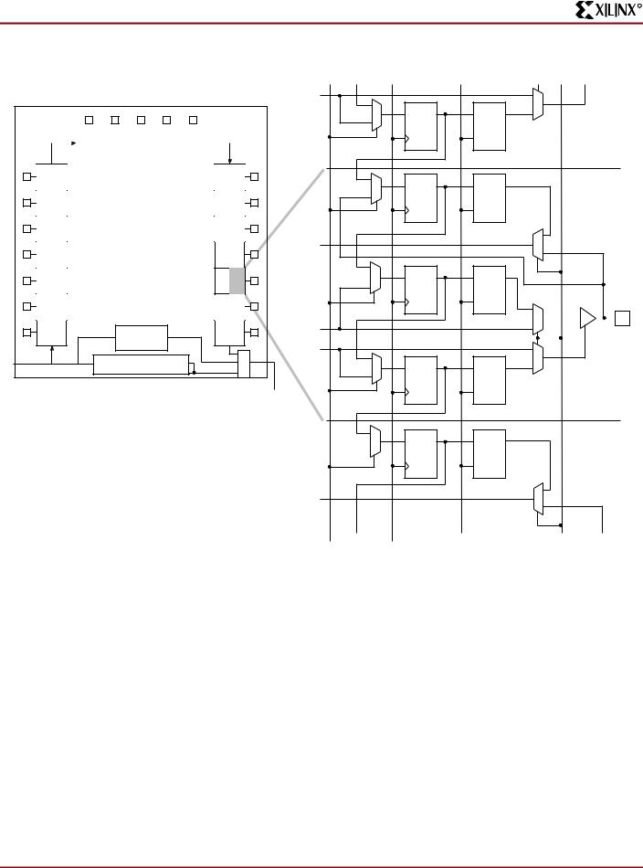
Spartan and Spartan-XL Families Field Programmable Gate Arrays
R
|
|
|
|
|
|
|
|
|
|
|
|
|
|
|
|
|
|
|
|
|
|
|
|
|
|
|
|
|
|
|
|
|
|
|
|
|
|
|
|
|
|
|
|
|
IOB |
IOB |
IOB |
IOB |
IOB |
|
|||||||||||||||
|
|
||||||||||||||||||||
|
|
|
|
|
|
|
|
|
|
|
|
|
|
|
|
|
|
|
|
|
|
IOB |
IOB |
IOB |
IOB |
IOB |
IOB |
IOB |
IOB |
IOB |
|
IOB |
IOB |
|
IOB |
IOB |
BYPASS |
IOB |
|
|
|
|
REGISTER |
|
M TDO TDI 
 INSTRUCTION REGISTER U
X
DATA IN
IOB.T |
|
|
|
|
|
0 |
|
|
|
|
|
|
|
|
1 |
|
|
sd |
|
1 |
|
D |
Q |
D |
|
Q |
|
|
|
|
||||
|
0 |
|
|
|
|
|
|
|
|
LE |
|
|
|
|
1 |
Q |
D |
sd |
Q |
|
|
D |
|
|
|||
|
0 |
|
|
|
|
|
|
|
|
LE |
|
|
|
IOB.I |
|
|
|
|
|
1 |
|
|
|
|
|
0 |
|
|
|
|
|
|
|
|
|
1 |
|
|
sd |
|
|
|
D |
Q |
D |
|
Q |
|
|
0 |
|
|
|
|
|
|
|
|
LE |
|
|
|
|
|
|
|
|
|
1 |
IOB.Q |
|
|
|
|
|
0 |
|
|
|
|
|
|
|
IOB.T |
|
|
|
|
|
0 |
|
|
|
|
|
|
|
|
1 |
|
|
sd |
|
1 |
|
D |
Q |
D |
|
Q |
|
|
0 |
|
|
|
|
|
|
|
|
LE |
|
|
|
|
1 |
|
|
sd |
|
|
|
D |
Q |
D |
|
Q |
|
|
0 |
|
|
|
|
|
|
|
|
LE |
|
|
|
IOB.I |
|
|
|
|
|
1 |
|
|
|
|
|
0 |
|
|
|
|
|
|
|
|
DATAOUT |
|
UPDATE |
|
|
EXTEST |
|
SHIFT/ |
CLOCK DATA |
|
|
|
|
|
CAPTURE |
REGISTER |
|
|
|
|
|
|
|
|
|
|
|
DS060_20_080400 |
Figure 20: Spartan/XL Boundary Scan Logic
22 |
www.xilinx.com |
DS060 (v1.6) September 19, 2001 |
|
1-800-255-7778 |
Product Specification |
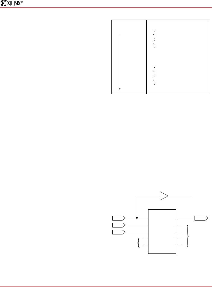
R
Spartan and Spartan-XL Families Field Programmable Gate Arrays
Table |
12: Boundary Scan Instructions |
|
|||
Instruction |
Test |
TDO |
I/O Data |
||
|
|
|
|||
I2 |
I1 |
I0 |
Selected |
Source |
Source |
|
|
|
|
|
|
0 |
0 |
0 |
EXTEST |
DR |
DR |
|
|
|
|
|
|
0 |
0 |
1 |
SAMPLE/ |
DR |
Pin/Logic |
|
|
|
PRELOAD |
|
|
|
|
|
|
|
|
0 |
1 |
0 |
USER 1 |
BSCAN. |
User Logic |
|
|
|
|
TDO1 |
|
|
|
|
|
|
|
0 |
1 |
1 |
USER 2 |
BSCAN. |
User Logic |
|
|
|
|
TDO2 |
|
|
|
|
|
|
|
1 |
0 |
0 |
READBACK |
Readback |
Pin/Logic |
|
|
|
|
Data |
|
|
|
|
|
|
|
1 |
0 |
1 |
CONFIGURE |
DOUT |
Disabled |
|
|
|
|
|
|
1 |
1 |
0 |
IDCODE |
IDCODE |
- |
|
|
|
(Spartan-XL |
Register |
|
|
|
|
only) |
|
|
|
|
|
|
|
|
1 |
1 |
1 |
BYPASS |
Bypass |
- |
|
|
|
|
Register |
|
|
|
|
|
|
|
Bit Sequence
The bit sequence within each IOB is: In, Out, 3-state. The input-only pins contribute only the In bit to the boundary scan I/O data register, while the output-only pins contributes all three bits.
The first two bits in the I/O data register are TDO.T and TDO.O, which can be used for the capture of internal signals. The final bit is BSCANT.UPD, which can be used to drive an internal net. These locations are primarily used by Xilinx for internal testing.
From a cavity-up view of the chip (as shown in the FPGA Editor), starting in the upper right chip corner, the boundary scan data-register bits are ordered as shown in Figure 21. The device-specific pinout tables for the Spartan/XL devices include the boundary scan locations for each IOB pin.
Bit 0 ( TDO end) Bit 1
Bit 2
(TDI end)
TDO.T
TDO.O
Top-edge IOBs (Right to Left) Left-edge IOBs (Top to Bottom)
MODE.I
Bottom-edge IOBs (Left to Right)
Right-edge IOBs (Bottom to Top)
BSCANT.UPD
DS060_21_080400
Figure 21: Boundary Scan Bit Sequence
BSDL (Boundary Scan Description Language) files for Spartan/XL devices are available on the Xilinx website in the File Download area. Note that the 5V Spartan devices and 3V Spartan-XL devices have different BSDL files.
Including Boundary Scan in a Design
If boundary scan is only to be used during configuration, no special schematic elements need be included in the schematic or HDL code. In this case, the special boundary scan pins TDI, TMS, TCK and TDO can be used for user functions after configuration.
To indicate that boundary scan remain enabled after configuration, place the BSCAN library symbol and connect the TDI, TMS, TCK and TDO pad symbols to the appropriate pins, as shown in Figure 22.
|
Optional |
|
To User |
|
|
|
|
|
|
|
Logic |
|
|
IBUF |
|
|
BSCAN |
|
|
TDI |
TDI |
TDO |
TDO |
TMS |
TMS |
DRCK |
|
TCK |
TCK |
IDLE |
To User |
|
|
|
|
From |
TDO1 |
SEL1 |
Logic |
|
|
|
|
User Logic |
TDO2 |
SEL2 |
|
|
|
||
DS060_22_080400
Figure 22: Boundary Scan Schematic Example
DS060 (v1.6) September 19, 2001 |
www.xilinx.com |
23 |
Product Specification |
1-800-255-7778 |
|
Spartan and Spartan-XL Families Field Programmable Gate Arrays
R
Even if the boundary scan symbol is used in a schematic, the input pins TMS, TCK, and TDI can still be used as inputs to be routed to internal logic. Care must be taken not to force the chip into an undesired boundary scan state by inadvertently applying boundary scan input patterns to these pins. The simplest way to prevent this is to keep TMS High, and then apply whatever signal is desired to TDI and TCK.
Avoiding Inadvertent Boundary Scan
If TMS or TCK is used as user I/O, care must be taken to ensure that at least one of these pins is held constant during configuration. In some applications, a situation may occur where TMS or TCK is driven during configuration. This may cause the device to go into boundary scan mode and disrupt the configuration process.
To prevent activation of boundary scan during configuration, do either of the following:
•TMS: Tie High to put the Test Access Port controller in a benign RESET state.
•TCK: Tie High or Low— do not toggle this clock input.
For more information regarding boundary scan, refer to the Xilinx Application Note, "Boundary Scan in FPGA Devices. "
Boundary Scan Enhancements (Spartan-XL Only)
Spartan-XL devices have improved boundary scan functionality and performance in the following areas:
IDCODE: The IDCODE register is supported. By using the IDCODE, the device connected to the JTAG port can be determined. The use of the IDCODE enables selective configuration dependent on the FPGA found.
The IDCODE register has the following binary format:
vvvv:ffff:fffa:aaaa:aaaa:cccc:cccc:ccc1
where
c = the company code (49h for Xilinx)
a = the array dimension in CLBs (ranges from 0Ah for XCS05XL to 1Ch for XCS40XL)
f = the family code (02h for Spartan-XL family) v = the die version number (currently 0h)
Table 13: IDCODEs Assigned to Spartan-XL FPGAs
FPGA |
IDCODE |
|
|
XCS05XL |
0040A093h |
|
|
XCS10XL |
0040E093h |
|
|
XCS20XL |
00414093h |
|
|
XCS30XL |
00418093h |
|
|
XCS40XL |
0041C093h |
|
|
Configuration State: The configuration state is available to JTAG controllers.
Configuration Disable: The JTAG port can be prevented from configuring the FPGA.
TCK Startup: TCK can now be used to clock the start-up block in addition to other user clocks.
CCLK Holdoff: Changed the requirement for Boundary Scan Configure or EXTEST to be issued prior to the release of INIT pin and CCLK cycling.
Reissue Configure: The Boundary Scan Configure can be reissued to recover from an unfinished attempt to configure the device.
Bypass FF: Bypass FF and IOB is modified to provide DRCLOCK only during BYPASS for the bypass flip-flop, and during EXTEST or SAMPLE/PRELOAD for the IOB register.
Power-Down (Spartan-XL Only)
All Spartan/XL devices use a combination of efficient segmented routing and advanced process technology to provide low power consumption under all conditions. The 3.3V Spartan-XL family adds a dedicated active Low power-down pin (PWRDWN) to reduce supply current to 100 A typical. The PWRDWN pin takes advantage of one of the unused No Connect locations on the 5V Spartan device. The user must de-select the "5V Tolerant I/Os" option in the Configuration Options to achieve the specified Power Down current. The PWRDWN pin has a default internal pull-up resistor, allowing it to be left unconnected if unused.
VCC must continue to be supplied during Power-down, and
configuration data is maintained. When the PWRDWN pin is pulled Low, the input and output buffers are disabled. The inputs are internally forced to a logic Low level, including the MODE pins, DONE, CCLK, and TDO, and all internal pull-up resistors are turned off. The PROGRAM pin is not affected by Power Down. The GSR net is asserted during Power Down, initializing all the flip-flops to their start-up state.
PWRDWN has a minimum pulse width of 50 ns (Figure 23). On entering the Power-down state, the inputs will be disabled and the flip-flops set/reset, and then the outputs are disabled about 10 ns later. The user may prefer to assert the GTS or GSR signals before PWRDWN to affect the order of events. When the PWRDWN signal is returned High, the inputs will be enabled first, followed immediately by the release of the GSR signal initializing the flip-flops. About 10 ns later, the outputs will be enabled. Allow 50 ns after the release of PWRDWN before using the device.
24 |
www.xilinx.com |
DS060 (v1.6) September 19, 2001 |
|
1-800-255-7778 |
Product Specification |
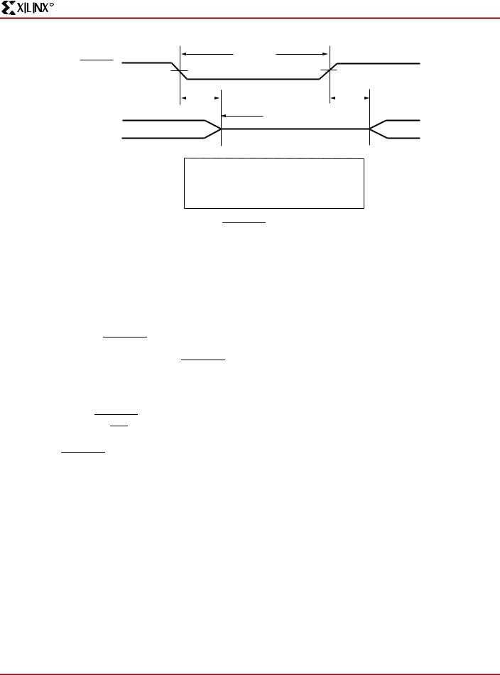
R
Spartan and Spartan-XL Families Field Programmable Gate Arrays
TPWDW
PWRDWN
50 ns |
|
|
|
50 ns |
|
|
Power Down Mode 
Outputs
Description |
Symbol |
Min |
|
|
|
Power Down Time |
TPWD |
50 ns |
Power Down Pulse Width |
TPWDW |
50 ns |
DS060_23_041901
Figure 23: PWRDWN Pulse Timing
Power-down retains the configuration, but loses all data stored in the device flip-flops. All inputs are interpreted as Low, but the internal combinatorial logic is fully functional. Make sure that the combination of all inputs Low and all flip-flops set or reset in your design will not generate internal oscillations, or create permanent bus contention by activating internal bus drivers with conflicting data onto the same long line.
During configuration, the PWRDWN pin must be High. If the Power Down state is entered before or during configuration, the device will restart configuration once the PWRDWN signal is removed. Note that the configuration pins are affected by Power Down and may not reflect their normal function. If there is an external pull-up resistor on the DONE pin, it will be High during Power Down even if the device is not yet configured. Similarly, if PWRDWN is asserted before configuration is completed, the INIT pin will not indicate status information.
Note that the PWRDWN pin is not part of the Boundary Scan chain. Therefore, the Spartan-XL family has a separate set of BSDL files than the 5V Spartan family. Boundary scan logic is not usable during Power Down.
Configuration and Test
Configuration is the process of loading design-specific programming data into one or more FPGAs to define the functional operation of the internal blocks and their interconnections. This is somewhat like loading the command registers of a programmable peripheral chip. Spartan/XL devices use several hundred bits of configuration data per CLB and its associated interconnects. Each
configuration bit defines the state of a static memory cell that controls either a function look-up table bit, a multiplexer input, or an interconnect pass transistor. The Xilinx development system translates the design into a netlist file. It automatically partitions, places and routes the logic and generates the configuration data in PROM format.
Configuration Mode Control
5V Spartan devices have two configuration modes.
•MODE = 1 sets Slave Serial mode
•MODE = 0 sets Master Serial mode
3V Spartan-XL devices have three configuration modes.
•M1/M0 = 11 sets Slave Serial mode
•M1/M0 = 10 sets Master Serial mode
•M1/M0 = 0X sets Express mode
In addition to these modes, the device can be configured through the Boundary Scan logic (See "Configuration Through the Boundary Scan Pins" on page 37.).
The Mode pins are sampled prior to starting configuration to determine the configuration mode. After configuration, these pin are unused. The Mode pins have a weak pull-up resistor turned on during configuration. With the Mode pins High, Slave Serial mode is selected, which is the most popular configuration mode. Therefore, for the most common configuration mode, the Mode pins can be left unconnected. If the Master Serial mode is desired, the MODE/M0 pin
should be connected |
directly to GND, or through a |
pull-down resistor of 1 KΩ |
or less. |
DS060 (v1.6) September 19, 2001 |
www.xilinx.com |
25 |
Product Specification |
1-800-255-7778 |
|
 Loading...