


XILINX XCR3128XL-7VQ100I, XCR3128XL-7VQ100C, XCR3128XL-7TQ144I, XCR3128XL-7TQ144C, XCR3128XL-7CS144I Datasheet
...
R
XCR3128XL 128 Macrocell CPLD
DS016 (v1.8) January 8, 2002 |
Preliminary Product Specification |
|
|
Features
•Lowest power 128 macrocell CPLD
•6.0 ns pin-to-pin logic delays
•System frequencies up to 145 MHz
•128 macrocells with 3,000 usable gates
•Available in small footprint packages
-144-pin TQFP (108 user I/O pins)
-144-ball CS BGA (108 user I/O)
-100-pin VQFP (84 user I/O)
•Optimized for 3.3V systems
-Ultra low power operation
-5V tolerant I/O pins with 3.3V core supply
-Advanced 0.35 micron five layer metal EEPROM process
-Fast Zero Power™ (FZP) CMOS design technology
•Advanced system features
-In-system programming
-Input registers
-Predictable timing model
-Up to 23 available clocks per function block
-Excellent pin retention during design changes
-Full IEEE Standard 1149.1 boundary-scan (JTAG)
-Four global clocks
-Eight product term control terms per function block
•Fast ISP programming times
•Port Enable pin for additional I/O
•2.7V to 3.6V supply voltage at industrial temperature range
•Programmable slew rate control per output
•Security bit prevents unauthorized access
•Refer to XPLA3 family data sheet (DS012) for architecture description
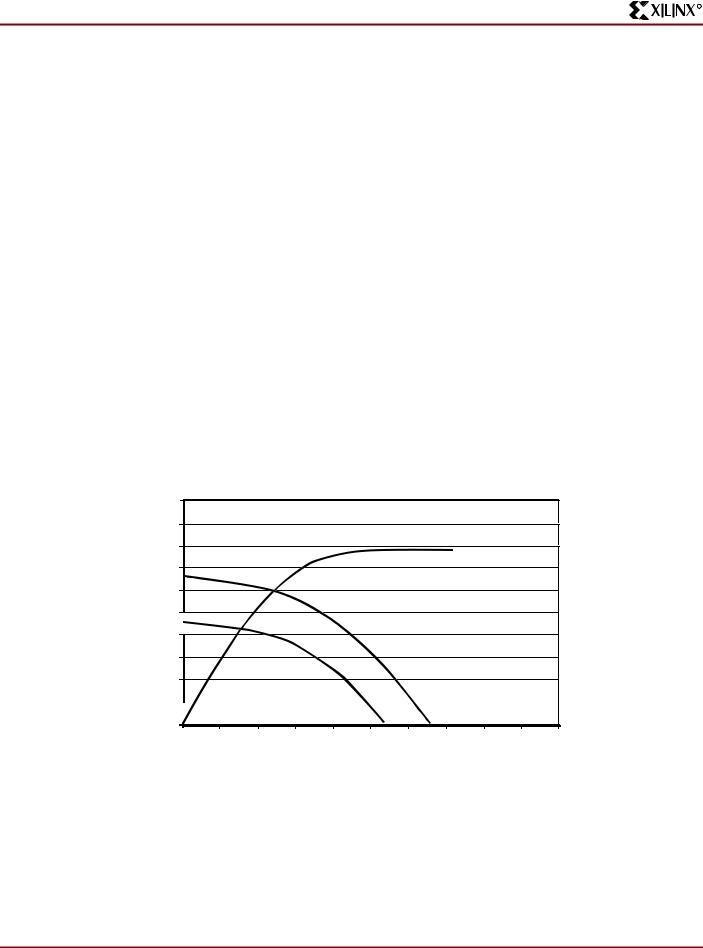
Table 1: Typical ICC vs. Frequency at VCC = 3.3V, 25° C
Description
The XCR3128XL is a 3.3V 128 macrocell CPLD targeted at power sensitive designs that require leading edge programmable logic solutions. A total of eight function blocks provide 3,000 usable gates. Pin-to-pin propagation delays are 6.0 ns with a maximum system frequency of 145 MHz.
TotalCMOS Design Technique for Fast Zero Power
Xilinx offers a TotalCMOS CPLD, both in process technology and design technique. Xilinx employs a cascade of CMOS gates to implement its sum of products instead of the traditional sense amp approach. This CMOS gate implementation allows Xilinx to offer CPLDs that are both high performance and low power, breaking the paradigm that to have low power, you must have low performance. Refer to Figure 1 and Table 1 showing the ICC vs. Frequency of our XCR3128XL TotalCMOS CPLD (data taken with eight resetable up/down, 16-bit counters at 3.3V, 25° C).
|
70 |
|
|
60 |
|
(mA) |
50 |
|
40 |
||
CC |
||
|
||
I |
20 |
|
Typical |
||
|
30 |
10
0
0 |
20 |
40 |
60 |
80 |
100 |
120 |
140 |
Frequency (MHz)
DS016_01_112100
Figure 1: Typical ICC vs. Frequency at VCC = 3.3V, 25° C
Frequency (MHz) |
0 |
1 |
5 |
10 |
20 |
40 |
60 |
80 |
100 |
120 |
140 |
|
|
|
|
|
|
|
|
|
|
|
|
Typical ICC (mA) |
0 |
0.5 |
2.2 |
4.4 |
8.7 |
17.1 |
25.3 |
33.6 |
41.6 |
49.7 |
57.7 |
© 2002 Xilinx, Inc. All rights reserved. All Xilinx trademarks, registered trademarks, patents, and disclaimers are as listed a t http://www.xilinx.com/legal.htm. All other trademarks and registered trademarks are the property of their respective owners. All specifications are subject to change without notice.
DS016 (v1.8) January 8, 2002 |
www.xilinx.com |
1 |
Preliminary Product Specification |
1-800-255-7778 |
|
XCR3128XL 128 Macrocell CPLD
R
DC Electrical Characteristics Over Recommended Operating Conditions(1)
Symbol |
Parameter |
Test Conditions |
Min. |
Max. |
Unit |
|
|
|
|
|
|
|
|
VOH(2) |
Output High voltage |
IOH = –8 mA |
2.4 |
- |
V |
|
VOL |
Output Low voltage for 3.3V outputs |
IOL = 8 mA |
- |
0.4 |
V |
|
IIL |
Input leakage current |
VIN = GND or VCC |
–10 |
10 |
A |
|
IIH |
I/O High-Z leakage current |
VIN = GND or VCC |
–10 |
10 |
A |
|
ICCSB |
Standby current |
VCC = 3.6V |
- |
100 |
A |
|
I |
Dynamic current(3,4) |
f = 1 MHz |
- |
1 |
mA |
|
CC |
|
|
|
|
|
|
|
|
|
f = 50 MHz |
- |
30 |
mA |
|
|
|
|
|
|
|
CIN |
Input pin capacitance(5) |
f = 1 MHz |
- |
8 |
pF |
|
CCLK |
Clock input capacitance(5) |
f = 1 MHz |
- |
12 |
pF |
|
CI/O |
I/O pin capacitance(5) |
f = 1 MHz |
- |
10 |
pF |
|
Notes:
1.See XPLA3 family data sheet (DS012) for recommended operating conditions.
2.See Figure 2 for output drive characteristics of the XPLA3 family.
3.See Table 1, Figure1 for typical values.
4.This parameter measured with a 16-bit, resetable up/down counter loaded into every function block, with all outputs disabled and unloaded. Inputs are tied to VCC or ground. This parameter guaranteed by design and characterization, not testing.
5.Typical values, not tested.
mA
100
90
OL (3.3V)
80
70
60
50
OH (3.3V)
40
30
OH (2.7V)
20
10
0
0 |
0.5 |
1 |
1.5 |
2 |
2.5 |
3 |
3.5 |
4 |
4.5 |
5 |
Volts
DS012_10_041901
Figure 2: Typical I/V Curve for the XPLA3 Family
2 |
www.xilinx.com |
DS016 (v1.8) January 8, 2002 |
|
1-800-255-7778 |
Preliminary Product Specification |

R
XCR3128XL 128 Macrocell CPLD
AC Electrical Characteristics Over Recommended Operating Conditions(1,2)
|
|
|
|
-6 |
|
-7 |
|
-10 |
|
|||
|
|
|
|
|
|
|
|
|
|
|
|
|
Symbol |
Parameter |
Min. |
|
Max. |
Min. |
|
Max. |
Min. |
|
Max. |
Unit |
|
|
|
|
|
|
|
|
|
|
|
|
|
|
TPD1 |
Propagation delay time (single p-term) |
- |
|
5.5 |
- |
|
7.0 |
- |
|
9.1 |
ns |
|
T |
PD2 |
Propagation delay time (OR array)(3) |
- |
|
6.0 |
- |
|
7.5 |
- |
|
10.0 |
ns |
|
|
|
|
|
|
|
|
|
|
|
|
|
|
|
|
|
|
|
|
|
|
|
|
|
|
TCO |
Clock to output (global synchronous pin clock) |
- |
|
4.0 |
|
|
5.0 |
- |
|
6.5 |
ns |
|
TSUF |
Setup time (fast input register) |
2.5 |
|
- |
3.0 |
|
- |
3.0 |
|
- |
ns |
|
TSU1(4) |
Setup time (single p-term) |
3.5 |
|
- |
4.3 |
|
- |
5.4 |
|
- |
ns |
|
TSU2 |
Setup time (OR array) |
4.0 |
|
- |
4.8 |
|
- |
6.3 |
|
- |
ns |
|
T |
(4) |
Hold time |
0 |
|
- |
0 |
|
- |
0 |
|
- |
ns |
|
H |
|
|
|
|
|
|
|
|
|
|
|
TWLH(4) |
Global Clock pulse width (High or Low) |
2.5 |
|
- |
3.0 |
|
- |
4.0 |
|
- |
ns |
|
TtPLH(4) |
P-term clock pulse width |
4.0 |
|
- |
5.0 |
|
- |
6.0 |
|
- |
ns |
|
T |
(4) |
Input rise time |
- |
|
20 |
- |
|
20 |
- |
|
20 |
ns |
|
R |
|
|
|
|
|
|
|
|
|
|
|
T |
(4) |
Input fall time |
- |
|
20 |
- |
|
20 |
- |
|
20 |
ns |
|
L |
|
|
|
|
|
|
|
|
|
|
|
fSYSTEM(4) |
Maximum system frequency |
- |
|
145 |
- |
|
119 |
- |
|
95 |
MHz |
|
T |
(4) |
Configuration time(5) |
- |
|
60 |
- |
|
60 |
- |
|
60 |
s |
|
CONFIG |
|
|
|
|
|
|
|
|
|
|
|
TINIT(4) |
ISP initialization time |
- |
|
60 |
- |
|
60 |
- |
|
60 |
s |
|
TPOE(4) |
P-term OE to output enabled |
- |
|
7.5 |
- |
|
9.3 |
- |
|
11.2 |
ns |
|
T |
(4) |
P-term OE to output disabled(6) |
- |
|
7.5 |
- |
|
9.3 |
- |
|
11.2 |
ns |
|
POD |
|
|
|
|
|
|
|
|
|
|
|
TPCO(4) |
P-term clock to output |
- |
|
6.5 |
- |
|
8.3 |
- |
|
10.7 |
ns |
|
TPAO(4) |
P-term set/reset to output valid |
- |
|
8.0 |
- |
|
9.3 |
- |
|
11.2 |
ns |
|
|
|
|
Advance |
|
|
Preliminary |
|
|
|
|||
|
|
|
|
|
|
|
|
|
|
|
|
|
Notes:
1.Specifications measured with one output switching.
2.See XPLA3 family data sheet (DS012) for recommended operating conditions.
3.See Figure 4 for derating.
4.These parameters guaranteed by design and/or characterization, not testing.
5.Typical current draw during configuration is 9 mA at 3.6V.
6.Output CL = 5 pF.
DS016 (v1.8) January 8, 2002 |
www.xilinx.com |
3 |
Preliminary Product Specification |
1-800-255-7778 |
|
 Loading...