


XC3190A-4PQ160C
XILINX XC3190A-4PQ160C, XC3190A-4PP175I, XC3190A-4PP175C, XC3190A-4PG175I, XC3190A-4PG175C Datasheet
...
November 9, 1998 (Version 3.1) 7-3
7
Features
• Complete line of four related Field Programmable Gate
Array product families
- XC3000A, XC3000L, XC3100A, XC3100L
• Ideal for a wide range of custom VLSI design tasks
- Replaces TTL, MSI, and other PLD logic
- Integrates complete sub-systems into a single
package
- Avoids the NRE, ti me del ay, and ris k of conv ent ional
masked gate arrays
• High-performance CMOS static memory technology
- Guaranteed toggle rates of 70 to 370 MHz, logic
delays from 7 to 1.5 ns
- System clock speeds over 85 MHz
- Low quiescent and active power consumption
• Flexible FPGA arch ite ctu re
- Compatible arrays ranging from 1,000 to 7,500 gate
complexity
- Extensive register, combinatorial, and I/O
capabilities
- High fan-out signal distribution, low-skew clock nets
- Internal 3-state bus capabilities
- TTL or CMOS input thresholds
- On-chip crystal oscillator amplifier
• Unlimited reprogrammability
- Easy design iteration
- In-system logi c changes
• Extensive packaging options
- Over 20 different packages
- Plastic and ceramic surface-mount and pin-grid-
array packages
- Thin and V ery Thin Quad Flat Pack (TQFP and
VQFP) options
• Ready for volu me production
- Standard, off-the-shelf product availability
- 100% factory pre-tested devices
- Excellent reliability record
• Complete Development System
- Schematic capture, automatic place and route
- Logic and timing simulation
- Interactive design editor for design optimization
- Timing calculator
- Interfaces to popular design environments like
Viewlogic, Cadence, Mentor Graphics, and others
Additional XC3100A Features
• Ultra-high-speed FPGA family with six memb e rs
- 50-85 MHz system clock rates
- 190 to 370 MHz guaranteed flip-flop toggle rates
- 1.55 to 4.1 ns logic delays
• High-end additional family member in the 22 X 22 CLB
array-size XC3195A device
• 8 mA output sink curr en t an d 8 mA so ur ce cur re nt
• Maximum power-down and quiescent current is 5 mA
• 100% architecture and pin-out compatible with other
XC3000 families
• Software and bitstream compatible with the XC3000,
XC3000A, and XC3000L families
XC3100A combines the features of the XC3000A and
XC3100 families:
• Additional interconnect resources for TBUF s and CE
inputs
• Error checking of the configuration bitstream
• Soft startup holds all outputs slew-rate limited during
initial power-up
• More advanced CMOS process
Low-Voltage Ver sions Available
• Low-voltage devices function at 3.0 - 3.6 V
• XC3000L - Low-voltage versions of XC3000A devices
• XC3100L - Low-voltage versions of XC3100A devices
0
XC3000 Series
Field Programmable Gate Arrays
(XC3000A/L, XC3100A/L)
November 9, 1998 (Version 3.1)
07*
Product Description
R
Device
Max Logic
Gates
Typical Gate
Range
CLBs Array
User I/Os
Max
Flip-Flops
Horizontal
Longlines
Configuration
Data Bits
XC3020A, 3020L, 3120A 1,500 1,000 - 1,500 64 8 x 8 64 256 16 14,779
XC3030A, 3030L, 3130A 2,000 1,500 - 2,000 100 10 x 10 80 360 20 22,176
XC3042A, 3042L, 3142A, 3142L 3,000 2,000 - 3,000 144 12 x 12 96 480 24 30,784
XC3064A, 3064L, 3164A 4,500 3,500 - 4,500 224 16 x 14 120 688 32 46,064
XC3090A, 3090L, 3190A, 3190L 6,000 5,000 - 6,000 320 16 x 20 144 928 40 64,160
XC3195A 7,500 6,500 - 7,500 484 22 x 22 176 1,320 44 94,984

R
XC3000 Series Field Programmable Gate Arrays
7-4 November 9, 1998 (Version 3.1)
Introduction
XC3000-Series Field Programmable Gate Arrays (FPGAs)
provide a group of high-performance, high-density, digital
integrated circuits. Their regular, extendable, flexible,
user-programmable array architecture is composed of a
configuration program store plus three types of config-
urable elements: a pe rimeter of I/O Blocks (IO Bs), a core
array of Configurable Logic Bocks (CLBs) and resources
for interconnection. The general structure of an FPGA is
shown in Figure 2. The development system provides
schematic capture and auto place-and-route for design
entry. Logic and timing simulation, and in-circuit emulation
are available as desig n verifi cation alternat ives. Th e design
editor is used for interactive design optimization, and to
compile the data pattern that represents the configuration
program.
The FPGA user logic functions and interconnections are
determined by the configuration program data stored in
internal st atic memory cells. The program can be loaded in
any of several modes to accommodate various system
requirements. The program data resides externally in an
EEPROM, EPROM or ROM on the application circuit
board, or on a flop py d isk o r har d di sk. O n-ch ip in itia liza tion
logic provides for optional automatic loading of program
data at power-up. The companion XC17XX Serial Configu-
ration PROMs provide a very simple serial configuration
program storage in a one-time programmable package.
The XC3000 Field Prog ramm able Ga te Array families p ro-
vide a variety of logic capacities, package styles, tempera-
ture ranges and speed grades.
XC3000 Series Overview
There are now four distinct family groupings within the
XC3000 Series of FPGA devices:
• XC3000A Family
• XC3000L Family
• XC3100A Family
• XC3100L Family
All four families share a common architecture, develop-
ment software, design and programming methodology, and
also common package pin-outs. An extensive Product
Description covers these common aspects.
Detailed parametric information for the XC3000A,
XC3000L, XC3100A, and XC3100L product families is then
provided. (The XC3000 and XC3100 families are not rec-
ommended for new designs.)
Here is a simple overview of those XC3000 products cur-
rently emphasized:
• XC3000A Family — The XC3000A is an enhanced
version of the basic XC3000 family, featuring additional
interconnect resources and other user-friendl y
enhancements.
• XC3000L Family — The XC3000L is identical in
architecture and features to the XC3000A family, but
operates at a nominal supply voltage of 3.3 V. The
XC3000L is the right solution for battery-operated and
low-power applications.
• XC3100A Family — The XC3100A is a
performance- optimized relative of the XC3000A family.
While both families are bitstream and footprint
compatible, the XC31 00A fa mily ex tends t oggle ra tes to
370 MHz and in-system performance to ov er 80 MHz.
The XC3100A famil y also offers one additional array
size, the XC3195A.
• XC3100L Family — The XC3100L is identical in
architectures and features to the XC3100A family, but
operates at a nominal supply volta ge of 3.3V.
Figure 1 illustrates the relationships betw een the families.
Compared to the original XC3000 family, XC3000A offers
additional fu nctiona lity and increas ed speed. The XC3000L
family offers the same additional functionality, but reduced
speed due to its lower supply voltage of 3.3 V. The
XC3100A family offers substantially higher speed and
higher density with the XC3195A.
New XC3000 Series Compared to Original
XC3000 Family
For readers already familiar with the original XC3000 family
of FPGAs, the major new features in the XC3000A,
XC3000L, XC3100A, and XC3100L families are listed in
this section.
All of these new families are upward-compatible extensions
of the original XC3000 FPGA architecture. Any bitstream
used to configure an XC30 0 0 d evic e will con fig ur e th e co r -
responding XC3000A, XC3000L, XC3100A, or XC3100L
device exactly the same way.
The XC3100A and XC3100L FPGA architectures are
upward-compatible extensions of the XC3000A and
XC3000L architec tures. A ny bits tream used to conf igure an
XC3000A or XC3000L device will configure the corre-
sponding XC3100A or XC3100L device exactly the same
way.
R
November 9, 1998 (Version 3.1) 7-5
XC3000 Series Field Programmable Gate Arrays
7
Improvements in the XC3000A and XC3000L
Families
The XC3000A and XC3000L families offer the following
enhancements over the popular XC3000 family:
The XC3000A and XC3000L families have additional inter-
connect resources to drive the I-inputs of TBUFs driving
horizontal Longlines. The CLB Clock Enable input can be
driven from a secon d verti cal Lon gline. These two addi tions
result in more efficient and faster designs when horizontal
Longlines are used for data bussing.
During configuration, the XC3000A and XC3000L devices
check the bit-stream format for stop bits in the appropriate
positions. Any error terminates the configuration and pulls
INIT Low.
When the configuration process is finished and the device
starts up in user mode , the first ac tivation of the outputs is
automatically slew-rate limited. This feature, called Soft
Startup, avoids the potential ground bounce when all
out-puts are turn ed on simultaneously. After start-up, the
slew rate of the indi vidual outputs i s, as in the XC 3000 fam-
ily, determined by the individual configuration option.
Improvements in the XC3100A and XC3100L
Families
Based on a more advanced CMOS process, the XC3100A
and XC3100L families are architecturally- identical, perfor-
mance-optimized relatives of the XC3000A and XC3000L
families. While all families are footprint compatible, the
XC3100A family extends achievable system performance
beyond 85 MHz.
XC3100
XC3100A
(XC3195A)
Gate Capacity
X7068
Functionality
XC3000L
XC3000A
XC3100L
Speed
Figure 1: XC3000 FPGA Families
R
XC3000 Series Field Programmable Gate Arrays
7-6 November 9, 1998 (Version 3.1)
Detailed Functional Description
The perimeter of configurable Input/Output Blocks (IOBs)
provides a programmable interface between the internal
logic array and the device package pins. The a rray of Con-
figurable Log ic Bloc ks (CLBs ) perfo rms user- specif ied log ic
functions. The interconnect resources are programmed to
form networks, carrying logic signals among blocks, analo-
gous to printed circuit board traces connecting MSI/SSI
packages.
The block logic functions are implemented by programmed
look-up table s. Fu nc t iona l opti o ns are i mp l ement ed b y pro -
gram-controlled multiplexers. Interconnecting networks
between blocks are implemented with metal segments
joined by program-controlled pass transistors.
These FPGA functions are established by a configuration
program which is loaded into an internal, distributed array
of configuration memory cells. The configuration program
is loaded into the device at power-up and may be reloaded
on command. The FPGA includes logic and control signals
to implement automatic or passive configuration. Program
data may be either bit serial or byte parallel. The develop-
ment system generates the configuration program bit-
stream used to configure the device. The memory loading
process is independent of the user lo gic functions.
Configuration Memory
The static mem ory cell used for t he config uration me mory
in the Field Programmable Gate Array has been designed
specifically for high reliability and n oise immunit y. Integrity
of the device con fig ur at i on me mor y bas ed o n th is d es ign i s
assured even under adverse conditions. As shown in
Figure 3, the basic memory cell consists of two CMOS
inverters pl us a p ass tr ansi stor used for w riti ng a nd rea ding
cell data. The cell is only written during configura tion and
only read during readback. During normal operation, the
cell provides continuous control and the pass transistor is
off and does not affect cell stability. This is quite different
from the operation of conventional memory devices, in
which the cells are frequently re ad and rewritten.
P9 P8 P7 P6 P5 P4 P3 P2 GNDPWR
DN
P11
P12
P13
U61
TCL
KIN
ADACABAA
3-State Buffers With Access
to Horizontal Long Lines
Configurable Logic
Blocks
Interconnect Area
BBBA
Frame Pointer
Configuration Memory
I/O Blocks
X3241
Figure 2: Field Programmable Gate Array Structure.
It consists of a perimeter of programmable I/O blocks, a core of configurable logic blocks and their interconnect resources.
These are all controlled by the distributed array of configuration program memory cells.
R
November 9, 1998 (Version 3.1) 7-7
XC3000 Series Field Programmable Gate Arrays
7
The memory cell outpu ts Q and Q use gr ound a nd V
CC
lev-
els and provide continuous, direct control. The additional
capacitive load together with the absence of address
decoding and sen se amp lifiers provid e high st ability to the
cell. Due to the structure of the configuration memory cells,
they are not affected by extreme power-supply excursions
or very high levels of alpha particle rad iation. In reliability
testing, no soft errors have been observed even in the
presence of very high doses of alpha radiation.
The method of loading the configuration data is selectable.
Two methods use serial data, while three use byte-wide
data. The internal configu ration log ic utilizes framin g infor-
mation, embedded i n the pro gram dat a by the developme nt
system, to direct memory-cell loading. The serial-data
framing and length-count preamble provide programming
compatibility for mixes of various FPGA device devices in a
synchronous, serial, daisy-chain fashion.
I/O Block
Each user-conf igurabl e IOB show n in Figur e 4, prov ides an
interface between the external package pin of the device
and the internal user logic. Each IOB includes both regis-
tered and direc t in put pat hs. Each I OB pro vides a pr ogram-
mable 3-state output buffer, which may be driven by a
registered or direct output signal. Configuration options
allow each IOB an inversion, a controlled slew rate and a
high impedance pull-up. Each input circuit also provides
input clamping diodes to provide electrostatic protection,
and circuits to inhibit latch-up produced by input currents.
Q
Data
Read or
Write
Configuration
Control
Q
X5382
Figure 3: Static Configuration Memory Cell.
It is loaded with one bit of configuration program and con-
trols one program selection in the Field Programmable
Gate Array.
FLIP
FLOP
QD
R
SLEW
RATE
PASSIVE
PULL UP
OUTPUT
SELECT
3-STATE
INVERT
OUT
INVERT
FLIP
FLOP
or
LATCH
DQ
R
REGISTERED IN
DIRECT IN
OUT
3- STATE
(OUTPUT ENABLE)
TTL or
CMOS
INPUT
THRESHOLD
OUTPUT
BUFFER
(GLOBAL RESET)
CK1
X3029
I/O PAD
Vcc
PROGRAM-CONTROLLED MEMORY CELLS
PROGRAMMABLE INTERCONNECTION POINT or PIP
=
IKOK
Q
I
O
T
PROGRAM
CONTROLLED
MULTIPLEXER
CK2
Figure 4: Input/Output Block.
Each IOB includes input and output storage elements and I/O options selected by configuration memory cells. A choice
of two clocks is available on each die edge. The polarity of each clock line (not each flip-flop or latch) is programmable.
A clock line that triggers the flip-flop on the rising edge is an active Low Latch Enable (Latch transparent) signal and vic e
versa. Passive pull-up can only be enabled on inputs, not on outputs. All user inputs are programmed for TTL or CMOS
thresholds.

R
XC3000 Series Field Programmable Gate Arrays
7-8 November 9, 1998 (Version 3.1)
The input-buffer portion of each IOB provides threshold
detection to translate external signals applied to the pack-
age pin to internal logic levels. The global input-buffer
threshold of th e IOBs can be programme d to be compat ible
with either TTL or CMOS levels . The buffered input sign al
drives the data input of a storage element, which may be
configured as either a flip-flop or a latch. The clocking
polarity (rising/falling edge-triggered flip-flop, High/Low
transparent latch) is programmable for each of the two
clock lines on each of the four die edges. Note that a clock
line driving a
rising
edge-triggered f l ip- flo p mak es any l a tch
driven by the sa me line on the same edge Low-level trans-
parent and vice vers a (
falling
edge,
High
transparent). All
Xilinx primitives in the supported schematic-entry pack-
ages, however, are positive edge-triggered flip-flops or
High transparent latches. When one clock line m ust drive
flip-flops as well as latch es, it is nec essary to c ompensa te
for the difference in clocking polarities with an additional
inverter either in the flip-flop clock input or the latch-enable
input. I/O storage elements are reset during configuration
or by the active-Low chip RESET
input. Both direct inp ut
(from IOB pi n I) a nd regi stered input (from IOB pi n Q) s ig-
nals are available for interconnect.
For reliable operation, inputs should have transition times
of less than 100 ns and should not be left floating. Floating
CMOS input-pin circuits might be at threshold and produce
oscillations. This can p roduce add itional pow er dissip ation
and system noise. A typical hysteresis of about 300 mV
reduces sensitivity to input noise. Each user IOB includes a
programmable high-impedance pull-up resistor, which may
be selected by the pro gram to prov ide a consta nt High for
otherwise undriven package pins. Although the Field Pro-
grammable Gate Array provides circuitry to provide input
protection for electrostatic discharge, normal CMOS han-
dling precautions should be observed.
Flip-flop loop delay s for the IOB and logic-bloc k flip-flops
are short, providing good performance under asynchro-
nous clock and dat a conditi ons. Shor t loop del ays minimi ze
the probability of a metastable condition that can result
from assertion of the clock during data transitions. Because
of the short-loop -de lay ch arac terist ic in th e Fie ld Pr ogr am-
mable Gate Ar ray, the IOB flip-flops can be used to syn-
chronize external signals applied to the device. Once
synchronized in the IOB, the signals can be used internally
without further consideration of their clock relative timing,
except as it applies to the internal logic and routing-path
delays.
IOB output buffers provide CMOS-compatible 4-mA
source-or-sink drive for high fan-out CMOS or TTL- com-
patible signal levels (8 mA in the XC3100A family ). The net-
work driving IOB pin O becomes the registered or direct
data source for the output buffer. The 3-state control signal
(IOB) pin T can control output activity. An open-drain output
may be obtained by using the same signal for driving the
output and 3-state signal nets so that the buffer output is
enabled only for a Low.
Configuration pr ogram bits for each IOB control featu res
such as optional output register, logic signal inversion, and
3-state and slew-rate control of the output.
The program-controlled memory cells of Figure 4 control
the following options.
• Logic inversion of the output is controlled by one
configuration program bit per IOB.
• Logic 3-state control of each IOB output buffer is
determined by the states of configuration progr am bits
that turn the bu ffer on, or off, or select the output buffer
3-state control interconnection (IOB pin T). When this
IOB output con tr ol s ign al i s Hig h, a l og ic o ne, t he buf f er
is disabled and the package pin is hig h impedance.
When this IOB outp ut contr ol signa l is Low, a logic ze ro,
the buffer is enabled and the package pin is active.
Inversion of the buffer 3-state control-logic sense
(output enable) is controlled by an additional
configuration program bit.
• Direct or registered output is selectable for each IOB.
The register us es a posit ive-e dge, clo cked f lip- flo p. The
clock source may be supplied (IOB pin OK) by either of
two metal lines available along each die edge. Each of
these lines is driven by an invertible buffer.
• Increased output transition s peed can be selected to
improve critical timing. Slower transiti ons reduce
capacitive-load peak currents of non-critical outputs
and minimize system noise.
• An internal high-impedance pull-up resistor (active by
default) prevents unconnected inputs from floating.
Unlike the original XC3000 series, the XC3000A,
XC3000L, XC3100A, and XC3100L families include the
Soft Startup feature. When the configuration process is fin-
ished and the device starts up in user mode, the first activa-
tion of the o utputs is automa tically slew-rate lim ited. This
feature avoids potential ground bounce when all outputs
are turned on sim ultaneously. After start-up, the sle w rate
of the individual outputs is determined by the individual
configuration option.
Summary of I/O Options
• Inputs
-Direct
- Flip-flop/latch
- CMOS/TTL threshold (chip inputs)
- Pull-up resistor/open circui t
• Outputs
- Direct/regi stered
- Inverted/not
- 3-state/on/off
- Full speed/slew limited
- 3-state/output enable (inverse)
R
November 9, 1998 (Version 3.1) 7-9
XC3000 Series Field Programmable Gate Arrays
7
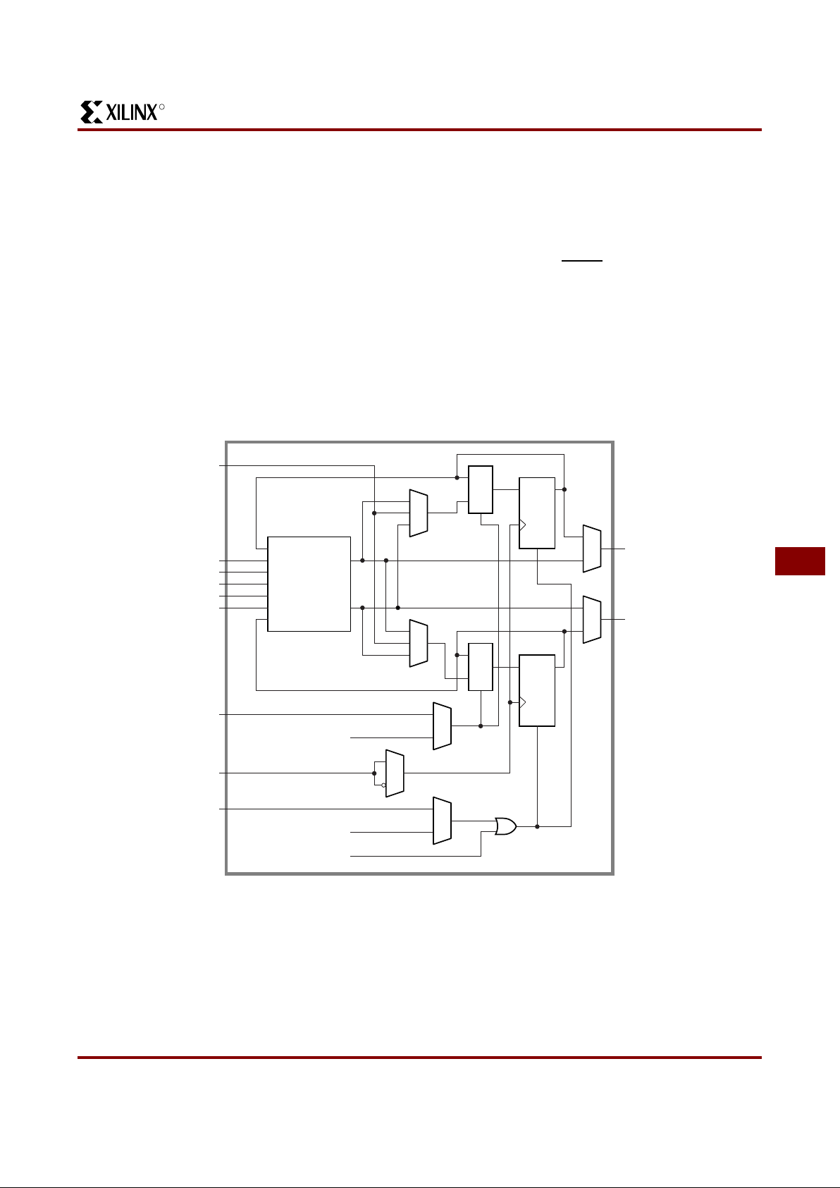
Configurabl e Logic Block
The array of CLBs provides the functional elements from
which the user’s logic is constructed. The logic blocks are
arranged in a matrix within the perimeter of IOBs. For
example, the XC3020A has 64 such blocks arranged in 8
rows and 8 colu mns. The devel opment system is used to
compile the confi guration data which is to be loaded into
the internal configuration memory to define the operation
and interconnection of each block. User definition of CLBs
and their interconnecting networks may be done by auto-
matic transla tion from a sche matic-cap ture logi c diagram or
optionally by installing library or user macros.
Each CLB has a combina torial logic sect ion, two flip -flops,
and an internal control section. See Figure 5. There are:
five logic inputs (A, B, C, D and E); a common clock input
(K); an asynchronous direct RESET input (RD); and an
enable clock (EC). All may be driven from the interconnect
resources adjacent to the blocks. Each CLB also has two
outputs (X and Y) which may drive interconnect networks.
Data input for either flip -flop within a CLB is su pplied from
the function F or G outp uts of th e combin atorial logic, or the
block input, DI. Both flip-flops in each CLB share the asyn-
chronous RD which, when enabled and High, is dominant
over clocked inputs. All flip-flops are reset by the
active-Low chip input, RESET
, or during the configuration
process. The flip-flops share the enable clock (EC) which,
when Low, recirculates the flip-flops’ present states and
inhibits response to the data-in or combinatorial function
inputs on a CLB. The user may enable these control i nputs
and select their sources. The user may also select the
clock net input (K), as well as its active sense within each
CLB. This programmable inversion eliminates the need to
route both phases of a clock signal throughout the device.
Q
COMBINATORIAL
FUNCTION
LOGIC
VARIABLES
D
RD
G
F
DIN
F
G
QX
QY
DIN
F
G
G
QY
QX
F
QD
RD
ENABLE CLOCK
CLOCK
DIRECT
RESET
1 (ENABLE)
A
B
C
D
E
DI
EC
K
RD
Y
X
X3032
0 (INHIBIT)
(GLOBAL RESET)
CLB OUTPUTS
DATA IN
0
1
0
1
MUX
MUX
Figure 5: Configurable Logic Block.
Each CLB includes a co m bi nato rial lo gic se ct ion , two flip - flops an d a p rogr am me m o ry co nt ro lled mu ltip lex er se le ction of
function. It has the following:
- five logic variable inputs A, B, C, D, and E
- a direct data in DI
- an enable clock EC
- a clock (invertible) K
- an asynchronous direct RESET RD
- two outputs X and Y
R
XC3000 Series Field Programmable Gate Arrays
7-10 November 9, 1998 (Version 3.1)
Flexible routing allows use of common or individual CLB
clocking.
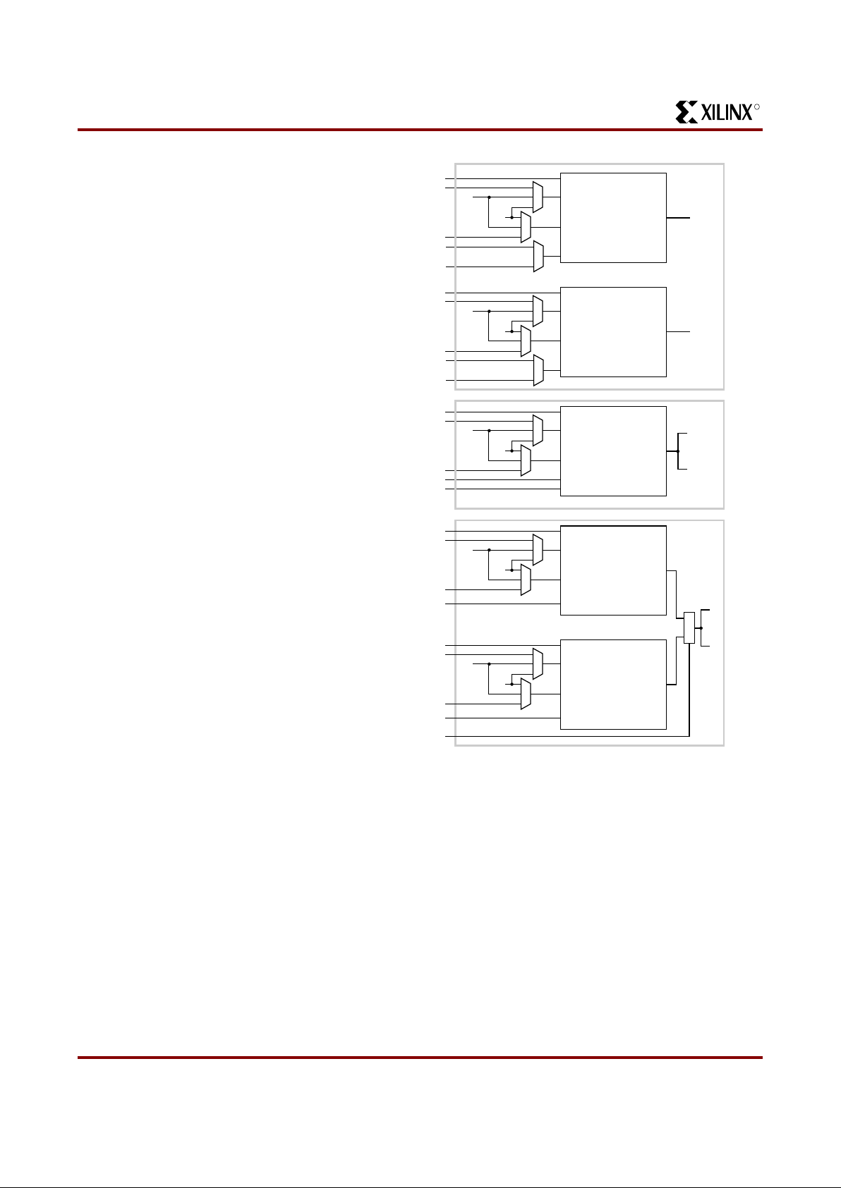
The combinatorial-logic portion of the CLB uses a 32 by 1
look-up table to implement Boolean functions. Variables
selected from the five logic inputs and two internal block
flip-flops are used as table address inputs. The combinato-
rial propagation delay through the network is independent
of the logic functi on generated and is spike fre e for single
input variable changes. This technique can generate two
independent logic functions of up to four variables each as
shown in Figure 6a, or a single function of five variables as
shown in Figure 6b , or some function s of seven variables
as shown in Figu re 6c. Figure 7 shows a modulo-8 binary
counter with paralle l enab le. It uses one CLB of each typ e.
The partial functio ns of six or seven variables are imple-
mented using the input variable (E) to dynamically select
between two functions of four different variables. For the
two functions of four variables each, the independent
results (F and G) may be used as data inputs to either
flip-flop or either logic block output. For the single function
of five variables and merged functions of six or seven vari-
ables, the F and G out put s are ide nti cal. Symmetr y of t he F
and G functions and the flip-flops allows the intercha nge of
CLB outputs to optimiz e routing eff icienc ies of th e networ ks
interconnecting the CLBs and IOBs.
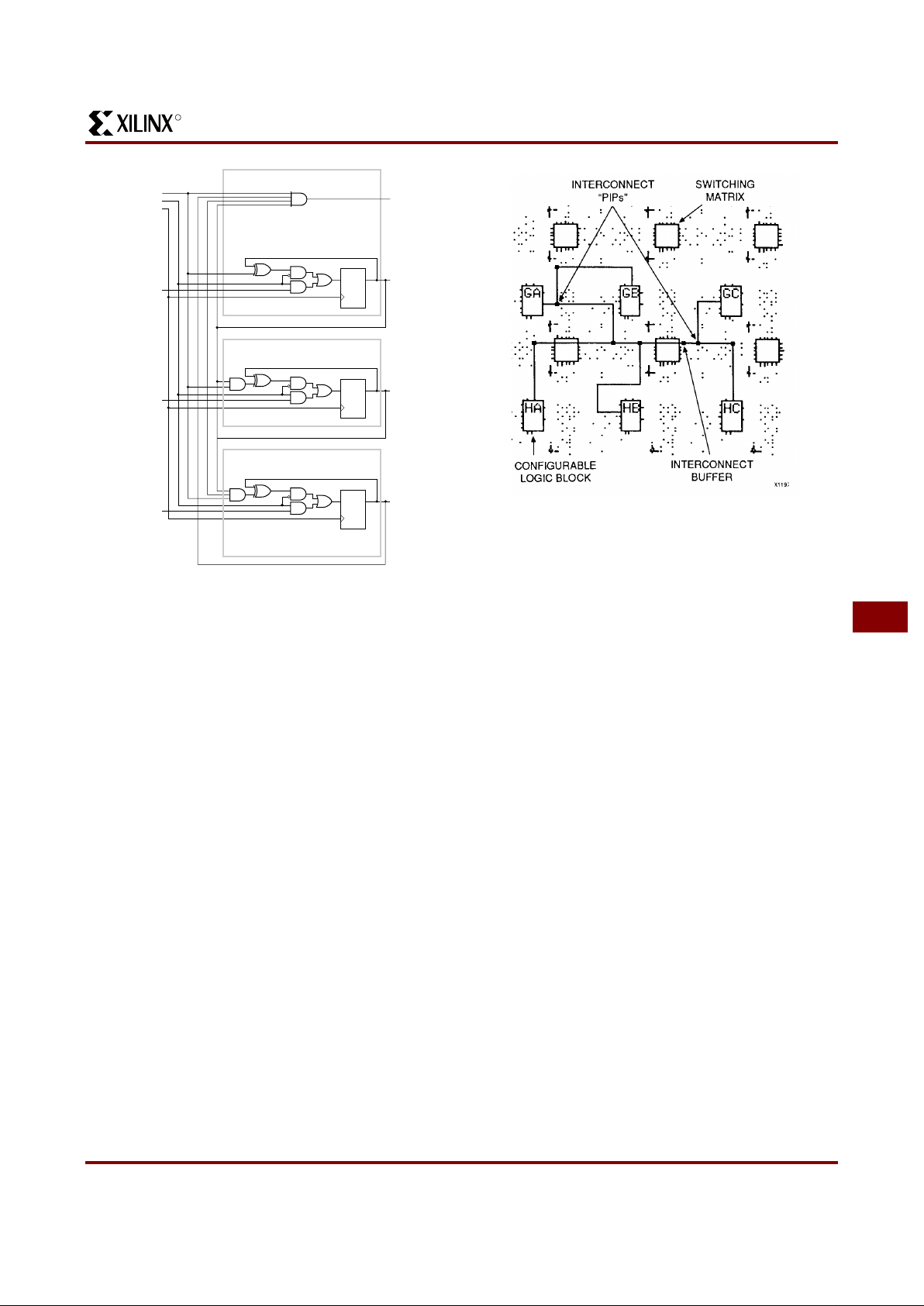
Programmable Interconnect
Programmable-interconnection resources in the Field Pro-
grammable Gate Array provide routing paths to connect
inputs and outputs of the IOBs and CLBs into logic net-
works. Inter connect ions bet ween b locks are com posed of a
two-layer grid of metal segments. Specially designed pass
transistors, each controlled by a configuration bit, form pro-
grammable interconnect points (PIPs) and switching matri-
ces used to implem ent the n ecessary connec tions be tween
selected metal segments and block pins. Figure 8 is an
example of a routed ne t. The develop ment system pr ovides
automatic routing of these interconnections. Interactive
routing is also available for d esign optimization. The inputs
of the CLBs or IOBs are mu ltiplexers which can be pro-
grammed to select an input network from the adjacent
interconnect segments.
Since the switch connections to
block inputs are unidirectional, as are block outputs,
they are usabl e only for block input connect ion and n ot
for routing.
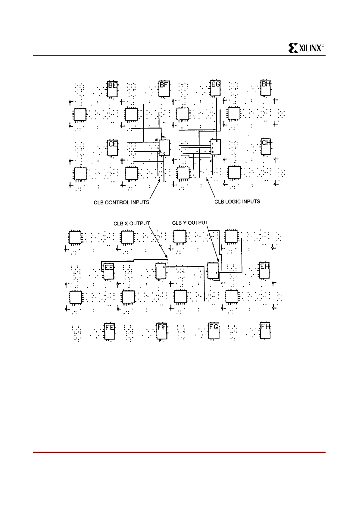
Figure 9 illustrates routing access to logic
block input variables, control inputs and block outputs.
Three types of metal reso urce s ar e pr ovide d to acco mmo-
date various network interconnect requirements.
• General Purpos e Interconnect
• Direct Connection
• Longlines (mul tiplexed busses and wide AND gates)
QY
Any Function
of Up to 4
Variables
QY
Any Function
of Up to 4
Variables
QY
Any Function
of 5 Variables
QY
Any Function
of Up to 4
Variables
QY
Any Function
of Up to 4
Variables
5c
5b
5a
QX
QX
QX
QX
QX
A
B
C
D
A
B
C
D
E
E
A
B
C
D
E
D
A
B
C
D
C
A
B
M
U
X
F
G
F
G
F
G
E
X5442
FGM
Mode
Figure 6: Combinational Logic Options
6a. Combinatorial Logic Option FG generates two func-
tions of four variables each. One variable, A, must be
common to bot h fu nc t ions . Th e se cond a nd t hird v ar iab l e
can be any choice of B, C, QX and QY. The fourth vari-
able can be any choice of D or E.
6b. Combinatorial Logic Option F generates any function
of five vari ables : A, D , E and two choic es o ut of B, C, QX,
QY.
6c. Combinatorial Logic Option FGM allows variable E to
select betwee n two f unct ion s of four varia bles : Bot h hav e
common inputs A and D and any choice out of B, C, QX
and QY for the remaining two variables. Option 3 can
then implemen t som e f unc t ion s o f s ix or se ve n v ar iabl e s.
R
November 9, 1998 (Version 3.1) 7-11
XC3000 Series Field Programmable Gate Arrays
7
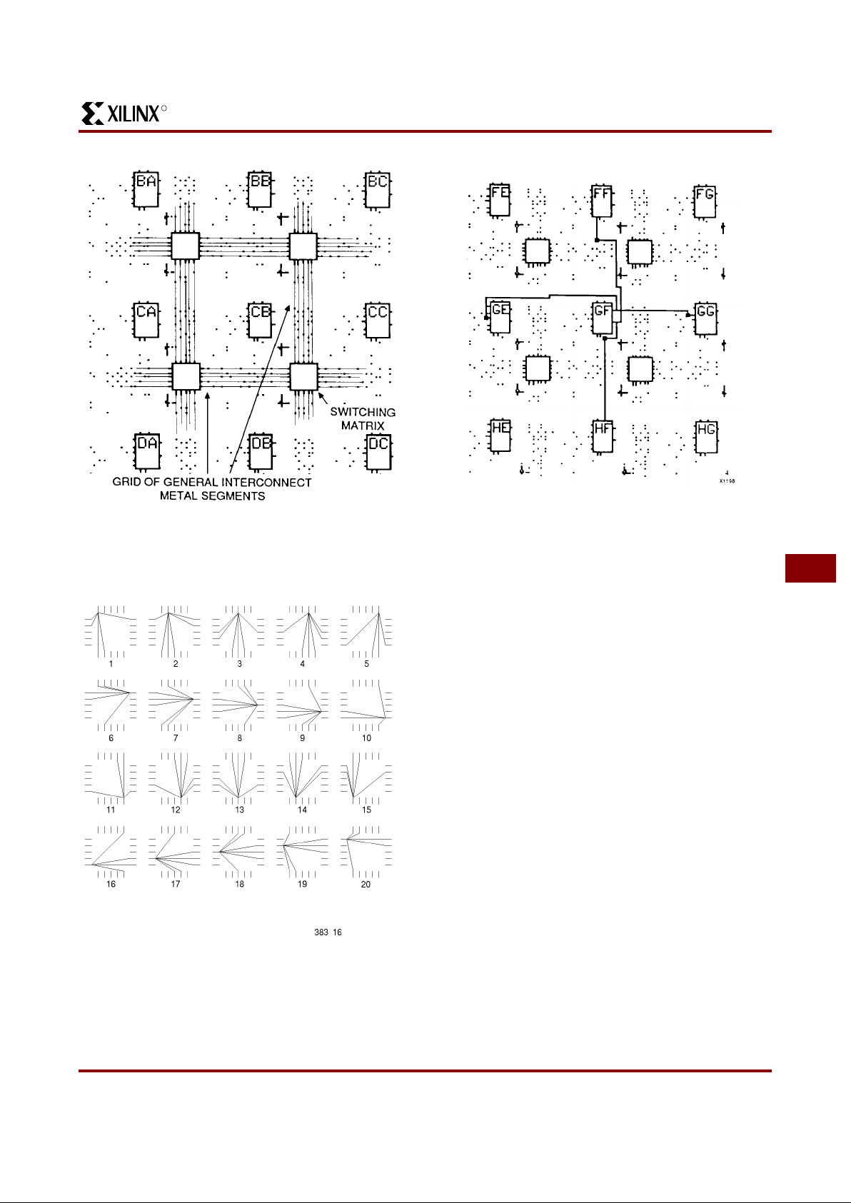
General Purpose Interconnect
General purpo se i nt er c onnec t, a s sho wn i n Fig ur e 10, c on -
sists of a grid of five horizontal and five vertical metal seg-
ments located between the rows and columns of logic and
IOBs. Each segment is the height or width of a logic block.
Switching matrices join the ends of these segments and
allow progra mmed inte rconnect ions bet ween t he metal grid
segments of adjo ining ro ws and co lumns. T he swit ches of
an unprogrammed device are all non-conducting. The con-
nections through the switch matrix may be established by
the automatic routing or by selecting the desired pairs of
matrix pins to be connected or disconnected. The legiti-
mate switching matrix combinations for each pin are indi-
cated in Figure 11.
Special buffers within th e general intercon nect areas pro-
vide periodic signal isolation and restoration for improved
performance of lengthy nets. The interconnect buffers are
available to pro pag at e s ign al s in ei ther di re cti o n on a giv en
general interconnect segment. These bidirectional (bidi)
buffers a re fou nd adjac ent to the switch ing ma tri ces, ab ove
and to the right. The other PIPs adjacent to the matrices
are accessed to or from Longlines. The development sys-
tem automatically defines the buffer direction based on the
location of the inte rconnection networ k source. The delay
calculator of the development system automatically calcu-
lates and dis plays the blo ck, i nte rcon nect a nd buf f er d elays
for any paths selected. Generation of the simulation netlist
with a worst-case delay model is provided.
Direct Interconnect
Direct interconn ect, sh own in Figure 12, provides the most
efficient implementation of networks between adjacent
CLBs or I/O Blocks. Signals routed from block to block
using the dir ect in terc onne ct ex hibit minim um inter conn ect
propagation and use no general interconnect resources.
For each CLB, the X output may be connected directly to
the B input of the CLB immediately to its right and to the C
input of the C LB to its le ft. The Y out put can use di rect in ter-
connect to driv e the D input of t he bloc k immed iat ely abo ve
and the A input of the block below. Direct interconnect
should be used to maximi ze the speed of high-perf ormance
portions of logic. Where logic blocks are adjacent to IOBs,
direct connect is provided alternately to the IOB inputs (I)
and outputs (O) on all four edges of the die. The right edge
provides additional direct connects from CLB outputs to
adjacent IOBs. Direct int erconnections of IOBs with CLBs
are shown in Figur e13.
D Q
D Q
D Q
Count Enable
Parallel Enable
Clock
D2
D1
D0
Dual Function of 4 Variables
Function of 6 Variables
Function of 5 Variables
Q2
Q1
Q0
FG
Mode
F
Mode
FGM
Mode
Terminal
Count
X5383
Figure 7: Counter.
The modulo-8 binary counter with parallel enable and
clock enable uses one combinatorial logic block of each
option.
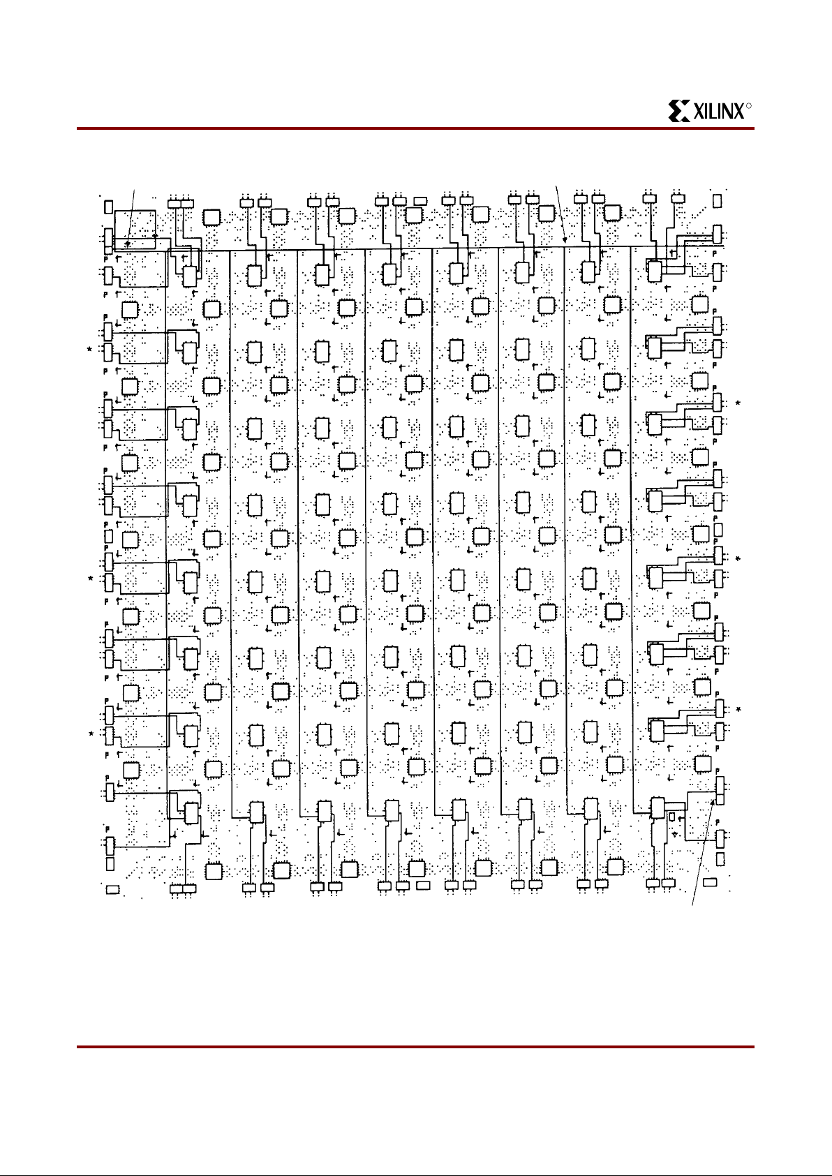
Figure 8: A Design Editor vi ew of rout ing reso urces
used to form a typical interconnection network from
CLB GA.
R
XC3000 Series Field Programmable Gate Arrays
7-12 November 9, 1998 (Version 3.1)
Figure 9: Design Edito r Loca tions of i nte rconnec t ac cess , CLB c ontrol i nputs, log ic i nputs and output s. Th e dot patt ern
represents the available programmable interconnection points (PIPs).
Some of the interconnect PIPs are directional.
R
November 9, 1998 (Version 3.1) 7-13
XC3000 Series Field Programmable Gate Arrays
7
Figure 10: FPGA General-Purpose Interconnect.
Composed of a grid of metal segments that may be inter-
connected throug h switch matrices to form networks for
CLB and IOB inputs and outputs.
Figure 1 1: Swi tch Ma trix Int erconne ctio n Options for
Each Pin.
Switch matrices on the edges are different.
Figure 12: CLB X and Y Outputs.
The X and Y outputs of each CLB have single contact,
direct access to inputs of adjacent CLBs
R
XC3000 Series Field Programmable Gate Arrays
7-14 November 9, 1998 (Version 3.1)
Figure 13: XC3020A Die-Edge IOBs. Th e XC3020A die-edge IOBs are provided with di rect access to adjacent CLBs.
Global Buffer Direct Input
Global Buffer Inerconnect
Alternate Buffer Direct Input
* Unbonded IOBs (6 Places)
R
November 9, 1998 (Version 3.1) 7-15
XC3000 Series Field Programmable Gate Arrays
7
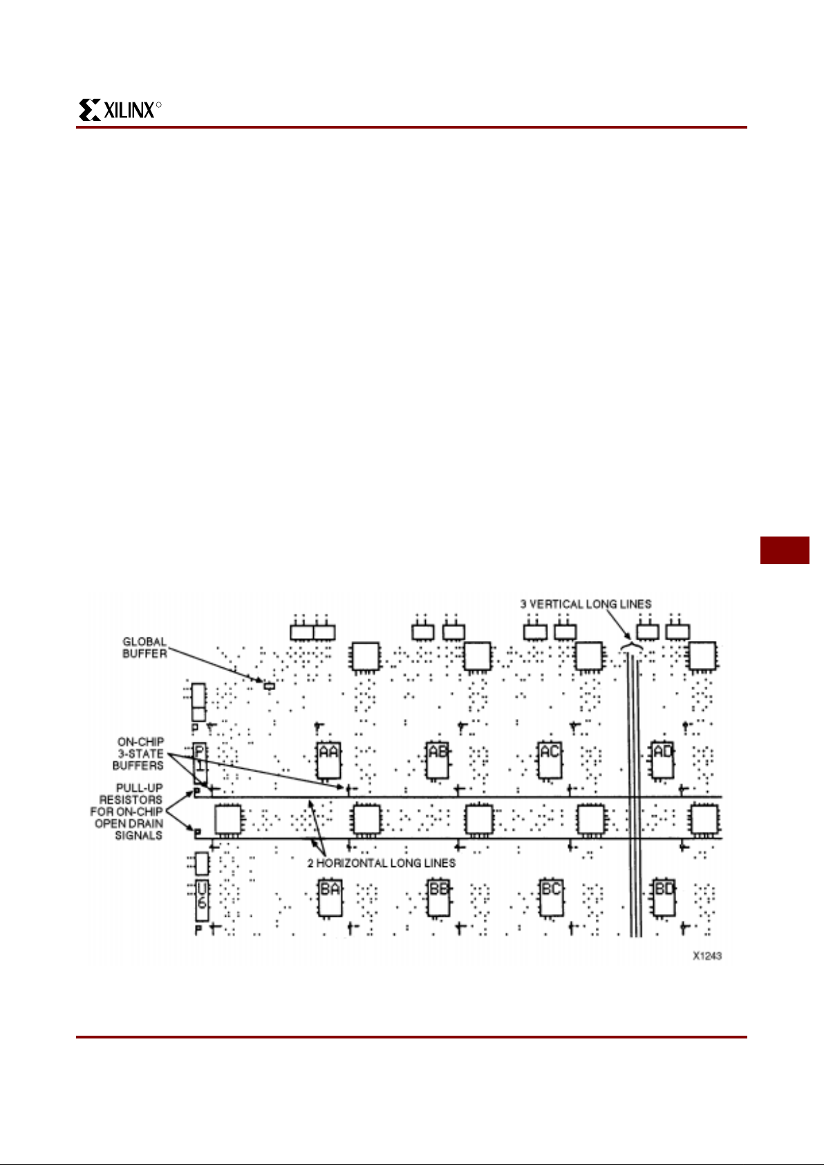
Longlines
The Longlines bypass the swit ch mat rices and are intend ed
primarily for signals that must travel a long distance, or
must have minimum skew among multiple destinations.
Longlines, shown in Figure 14, run vertically and horizo n-
tally the heig ht or width of the interco nnect area . Each inter -
connection column has three vertical Longlines, and each
interconnection row has two horizontal Longlines. Two
additional Longlines are located adjacent to the outer sets
of switching matrices. In devices larger than the XC3020A
and XC3120A FPGAs , two vertical Longlines in ea ch col-
umn are connectable half-length lines. On the XC3020A
and XC3120A FPGAs, only the outer Longlines are con-
nectable half-length lines.
Longlines can be dr i ve n by a l og ic blo ck or IOB out pu t on a
column-by-column bas is. This capability provides a com-
mon low skew contro l or clock line within each colu mn of
logic blocks. Interconnections of these Longlines are
shown in Figure 15. Isolation buffers are provided at each
input to a Longline and are enabled automatically by the
development system when a connection is made.
Figure 14: Horizontal and Vertical Longlines. These Longlines provide high fan-out, low-skew signal distribution in
each row and column. The global buf fer in the upper left die corner drives a common line throughout the FPGA.
R
XC3000 Series Field Programmable Gate Arrays
7-16 November 9, 1998 (Version 3.1)
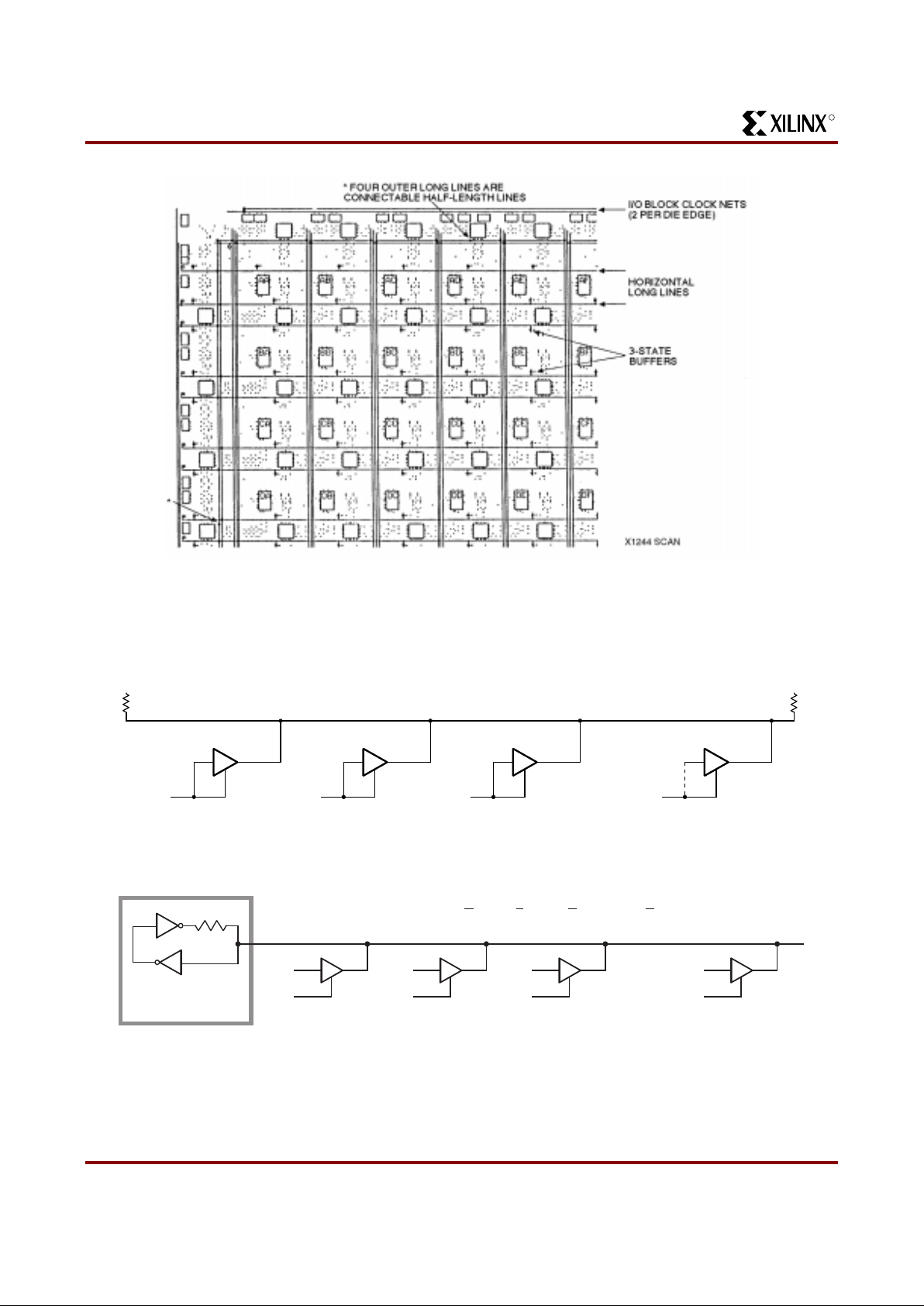
Figure 15: Programmable Interconnection of Longlines. This is provided at the edges of the routing area.
Three-state b uf f er s al low the us e of ho riz on ta l Lo ng l ines t o fo rm on- ch i p wir ed AND and mul t ipl e xe d b uses . The lef t t wo
non-clock vert ical Longlines per column (except XC3020A) and the outer perimeter Longlines may be programmed as
connectable half-length lines.
V
CC
D
A
D
B
D
C
D
N
V
CC
Z
=
D
A
•
D
B
•
D
C
•
...
•
D
N
X3036
(LOW)
Figure 16: 3-State Buffers Implement a Wired-AND Function. When all the buffer 3-state lines are High, (high
impedance), the pull-up resistor(s) provide the High output. The buffer inputs are driven by the control signals or a Low.
D
A
A
D
B
B
D
C
C
D
N
N
D
A
A•+=D
B
B•+D
C
C•+ D
N
N•Z…+
X1741A
WEAK
KEEPER CIRCUIT
Figure 17: 3-State Buff ers Implement a Multiplexer. The selection is accomplished by the buffer 3-state signal.
R
November 9, 1998 (Version 3.1) 7-17
XC3000 Series Field Programmable Gate Arrays
7
A buffer in the upper left corner of the FPGA chip drives a
global net which is availa ble to all K inputs of logic bloc ks.
Using the global buffer for a clock signal provides a
skew-free, high fan-out, synchronized clock for use at any
or all of the IOBs and CLBs. Configuration bits for the K
input to each logic block can select this global line or
another routing resource as the clock source for its
flip-flops. This net may also be pro grammed to drive the die
edge clock lines for IOB use. An enhanced speed, CMOS
threshold, di rect acces s to this b uffer is avail able at the s ec-
ond pad from the top of the left die edge.
A buffer in the lower right corner of the array drives a hori-
zontal Longline that can drive programmed connections to
a vertical Longline in each interconnection column. This
alternate buffer also has low skew and high fan-out. The
network formed by this alternate buffer’s Longlines can be
selected to drive th e K inputs of the CLBs. CMOS t hresh-
old, high speed access to this buffer is available from the
third pad from the bottom of the right die edge.
Internal Busses
A pair of 3-st ate buf fer s, lo cated a djacent to each CLB, per -
mits logic to drive the horizontal Longlines. Logic operation
of the 3-stat e buf fer con trols allows them t o implem ent wid e
multiplexing functions. Any 3-state buffer input can be
selected as drive for the horizontal long-line bus by apply-
ing a Low logic level on its 3-state control line. See
Figure 16. The user is required to avoid contention which
can result from multiple driver s with oppo sing logic levels.
Control of the 3-state input by the same signal that drives
the buffer input , cr eates a n open -drai n wi red-AN D func tio n.
A logic High on both buffer inputs creates a high imped-
ance, which rep res en t s n o cont en ti o n. A l ogic Lo w e nabl es
the buffer to dr i v e the Lon gl in e Lo w. See Fig ur e 17 . Pull-up
resistors are available at each end of the Longline to pro-
vide a High output when all connected buffers are non-con-
ducting. This forms fast, wide gating functions. When data
drives the inputs, and separate signals drive the 3-state
control lines, these buffers form multiplexers (3-state bus-
ses). In this case, care must be used to prevent contention
through multiple active buffers of conflicting levels on a
common line. Each horizontal Longline is also driven by a
weak keeper circuit that prevents undefined floating levels
by maintaining the p revious logi c level wh en th e line is not
driven by an active buffer or a pull-up resistor. Figure18
shows 3-state buffers, Longlines and pull-up resistors.
3-STATE CONTROL
GG
HG
P40 P41 P42 P43 RST
P46
.l
X1245
.q
.Q
OS
C
P47
BCL
KIN
P48
GH
HH
.lk
.ck
I/O CLOCKS
BIDIRECTIONAL
INTERCONNECT
BUFFERS
GLOBAL NET
3 VERTICAL LONG
LINES PER COLUMN
HORIZONTAL LONG LINE
PULL-UP RESISTOR
HORIZONTAL LONG LINE
OSCILLATOR
AMPLIFIER OUTPUT
DIRECTINPUT OF P47
TO AUXILIARY BUFFER
CRYSTAL OSCILLATOR
BUFFER
3-STATE INPUT
3-STATE BUFFER
ALTERNATE BUFFER
D
P
G
M
Figure 18: Design Editor.
An extra large view of possible interconnections in the lower right co rner of the XC3020A.
R
XC3000 Series Field Programmable Gate Arrays
7-18 November 9, 1998 (Version 3.1)
Crystal Oscillator
Figure 18 also sh ows th e l o cati o n o f an int er nal high s pe ed
inverting amplifier that may be used to implement an
on-chip crystal osc illator. It is associated wit h the au xiliary
buffer in the lower right corner of the die. When the oscilla-
tor is configured and connected as a signal source, two
special user IOBs are also configured to connect the oscil-
lator amplifier w ith external crystal oscillator c omponents
as shown in Figure 19. A divide by two option is available to
assure symmetry. The oscillator circuit becomes active
early in the configu ration process to allow the oscillat or to
stabilize. Actual internal co nnection is delayed until com-
pletion of configuration. In Figure 19 the feedback resistor
R1, between the output and input, biases the amplifier at
threshold. The in version of the a mplifier, together with the
R-C networks and an AT-cut series resonant crystal, pro-
duce the 360-degre e phase shif t of the Pierce os cillator. A
series resistor R2 may be included to add to the amplifier
output impedance when needed for phase-shift control,
crystal resistance ma tching, or to limit the amplifier input
swing to control clipping at large amplitudes. Excess feed-
back voltage may be corrected by the ratio of C2/C1. The
amplifier is designed to be used from 1 MHz to about
one-half the specified CLB toggle frequency. Use at fre-
quencies below 1 MHz may require individual characteriza-
tion with res pect to a ser ies resistance . Crystal osc illators
above 20 MHz generall y require a c rystal which oper ates in
a third overtone mode, where the fundamental frequency
must be suppressed by an inductor across C2, turning this
parallel resonant circuit to double the fundamental crystal
frequency, i.e., 2/3 of the desired third harmonic frequency
network. When the oscillator inverter is not used, these
IOBs and their package pins are available for general user
I/O.
Alternate
Clock Buffer
XTAL1
XTAL2
(IN)
R1
R2
Y1
C1 C2
Internal External
R1
R2
C1, C2
Y1
Suggested Component Values
0.5 – 1 MΩ
0 – 1 kΩ
(may be required for low frequency, phase
shift and/or compensation level for crystal Q)
10 – 40 pF
1 – 20 MHz AT-cut parallel resonant
X7064
68 PIN
PLCC
47
43
84 PIN
PLCC
57
53
PGA
J11
L11
132 PIN
PGA
P13
M13
160 PIN
PQFP
82
76
XTAL 1 (OUT)
XTAL 2 (IN)
100 PIN
CQFP
67
61
PQFP
82
76
164 PIN
CQFP
105
99
44 PIN
PLCC
30
26
175 PIN
PGA
T14
P15
208 PIN
PQFP
110
100
176 PIN
TQFP
91
85
D Q
Figure 19: Crystal Oscillator Inverter. When activated, and by selecting an output network for its bu ffer, the cryst al
oscillator inverter uses two unconfigured package pins and external components to implement an oscillator. An optional
divide-by-two mode is available to assure symmetry.
R
November 9, 1998 (Version 3.1) 7-19
XC3000 Series Field Programmable Gate Arrays
7
Configuration
Initialization Phase
An internal power-on-reset circuit is triggered when power
is applied. Wh en V
CC
reaches the voltage at which portions
of the FPGA device begin to operate (nominally 2.5 to 3 V),
the programmable I/O output buffers are 3-stated and a
high-impedance pull-up resistor is provided for the user
I/O pins. A time-out delay is initiated to allow the power
supply voltage to stabilize . During th is time the powe r-down
mode is inhibi t ed. Th e I n iti a li zati on s t at e ti me -o ut (a bo ut 11
to 33 ms) is determined by a 14-bit counter driven by a
self-generated internal timer. This nominal 1-MHz timer is
subject to variations with process, temperature and power
supply. As shown in Table 1, five configuration mode
choices are available as determined by the input levels of
three mode pins; M0, M1 an d M 2.
In Master configuration modes, the device becomes the
source of the Configuration Clock (CCLK). The beginning
of configuration of devices using Peripheral or Slave
modes must be delayed long enough for their initialization
to be completed. An FPGA with mode lines selecting a
Master configuration mode extends its initialization state
using four times the delay (43 to 130 ms) to assure that all
daisy-chained slave devices, which it may b e driving, will
be ready even if the master is very fast, and the slave(s)
very slow . Figu re 20 shows the state sequ ences. At the en d
of Initialization, the device enters the Clear state where it
clears the configuration memory. The active Low,
open-drain initialization signal INIT
indicates when th e Ini-
tialization and Clear states are complete. The FPGA tests
for the absence of an external active Low RESET
before it
makes a final sample of the mode lines and enters the Con-
figuration s tat e. An exte rna l wire d-A ND of one or more INIT
pins can be used to co ntrol config uration by the assertio n of
the active-Low RESET
of a master mode device or to sig-
nal a processor that the FPG A s ar e not y et initialized .
If a configuration has begun, a re-assertion of R ESET
for a
minimum of three in ternal timer cycles will be r ecognized
and the FPGA will initiate an ab ort, returning to the Clear
state to clear the partially loaded configuration memory
words. The FPGA will then resample RESET
and the mode
lines before re-ent er in g the Con fig ur ation state.
During configuration, the XC3000A, XC3000L, XC3100A,
and XC3100L devices check the bit-stream format for stop
bits in the appropr iate positions. Any erro r terminates the
configuration and pulls INIT Lo w.
Table 1: Configuration Mode Choices
M0 M1 M2 CCLK Mode Data
0 0 0 output Master Bit Serial
0 0 1 output Master Byte Wide Addr. = 0000 up
010— reserve d —
0 1 1 output Mas te r Byte Wide Addr. = FFFF down
1 0 0 — reserved —
1 0 1 output Peripheral Byte Wide
1 1 0 — reserved —
1 1 1 input Slave Bit Serial
All User I/O Pins 3-Stated with High Impedance Pull-Up, HDC=High, LDC=Low
Initialization
Power-On
Time Delay
Clear
Configuration
Memory
Test
Mode Pins
Configuration
Program Mode
Start-Up
Operational
Mode
Power Down
No HDC, LDC
or Pull-Up
No
X3399
INIT Output = Low
Clear Is
~ 200 Cycles for the XC3020A—130 to 400 µs
~ 250 Cycles for the XC3030A—165 to 500 µs
~ 290 Cycles for the XC3042A—195 to 580 µs
~ 330 Cycles for the XC3064A—220 to 660 µs
~ 375 Cycles for the XC3090A—250 to 750 µs
RESET
Active
PWRDWN
Inactive
PWRDWN
Active
Active RESET
Operates on
User Logic
Low on DONE/PROGRAM and RESET
Active RESET
Power-On Delay is
2
14
Cycles for Non-Master Mode—11 to 33 ms
2
16
Cycles for Master Mode—43 to 130 ms
Figure 20: A State Diagram of the Configuration Process for Power-up and Reprogram.
R
XC3000 Series Field Programmable Gate Arrays
7-20 November 9, 1998 (Version 3.1)
A re-program is i nitiated.when a configured XC3000 series
device senses a Hig h- to -L ow tr ans i ti on a nd s ubse que nt >6
µs Low level on the DONE/PROG
package pi n, or, if this
pin is external ly h el d p erm anent l y Low, a Hi gh -to- Low t ran -
sition and subse quent >6 µs Low time on the RESET
pack-
age pin.
The device returns to the Clear state where the configura-
tion memory is cleared and mode lines re-sampled, as for
an aborted configuration. The complete configuration pro-
gram is cleared and loaded during each configuration pro-
gram cycle.
Length count cont ro l allo ws a s yst em of multip le F ie l d Pr o-
grammable Gate Arrays, of assorted sizes, to begin op era-
tion in a synchronized fashion. The configuration program
generated by the development system begins with a pre-
a mb le of 111111110 0 10 fo ll ow e d b y a 24 -b i t l en gt h co un t
representing the total number of configuration clocks
needed to complete loading of the configuration pro-
gram(s). The data framing is shown in Figure 21. All
FPGAs connec ted in series read and shift preamble and
length count in on positive and o ut on negative c onfigura-
tion clock edges. A device which has received the pream-
ble and length count then presents a High Data Out until it
has intercepted the appropriate number of data frames.
When the configuration program memory of an FPGA is full
and the length count does not yet compare, the device
shifts any additional data through, as it did for preamble
and length count. When the FPGA configuration memory is
full and the length count co m pa res, the device will execute
11111111
0010
< 24-Bit Length Count >
1111
0 <Data Frame # 001 > 111
0 <Data Frame # 002 > 111
0 <Data Frame # 003 > 111
. . .
. . .
. . .
0 <Data Frame # 196 > 111
0 <Data Frame # 197 > 111
1111
—Dummy Bits*
—Preamble Code
—Configuration Program Length
—Dummy Bits (4 Bits Minimum)
For XC3120
197 Configuration Data Frames
(Each Frame Consists of:
A Start Bit (0)
A 71-Bit Data Field
Three Stop Bits
Postamble Code (4 Bits Minimum)
Header
Program Data
Repeated for Each Logic
Cell Array in a Daisy Chain
*The LCA Device Require Four Dummy Bits Min; Software Generates Eight Dummy Bits
X5300_01
Figure 21: Internal Configuration Data Structure for an FPGA. This shows the preamble, length count and data
frames generated by the Development Sy stem.
The Length Count produced by the program = [(40-bit preamble + sum of program data + 1 per daisy chain device)
rounded up to multiple of 8] – (2 ≤ K ≤ 4) where K is a function of DONE and RESET timing selected. An ad ditional 8 is
added if roundup increment is less than K. K additional clocks are needed to complete start-up after length count is
reached.
Device
XC3020A
XC3020L
XC3120A
XC3030A
XC3030L
XC3130A
XC3042A
XC3042L
XC3142A
XC3142L
XC3064A
XC3064L
XC3164A
XC3090A
XC3090L
XC3190A
XC3190L XC3195A
Gates 1,000 to 1,500 1,500 to 2,000 2,000 to 3,000 3,500 to 4,500 5,000 to 6,000 6,500 to 7,500
CLBs 64 100 144 224 320 484
Row x Col (8 x 8) (10 x 10) (12 x 12) (16 x 14) (20 x 16) (22 x 22)
IOBs 64 80 96 120 144 176
Flip-flops 256 360 480 688 928 1,320
Horizontal Longlines 16 20 24 32 40 44
TBUFs/Horizontal LL 9 11 13 15 17 23
Bits per Frame
(including1 start and 3 stop bits)
75 92 108 140 172 188
Frames 197 241 285 329 373 505
Program Data =
Bits x Frames + 4 bits
(excludes header)
14,779 22,176 30,784 46,064 64,160 94,944
PROM size (bits) =
Program Data
+ 40-bit Header
14,819 22,216 30,824 46,104 64,200 94,984
R
November 9, 1998 (Version 3.1) 7-21
XC3000 Series Field Programmable Gate Arrays
7
a synchronou s start -up s eque nce a nd become opera tio nal.
See Figure 22. Two CCLK cycles after the completion of
loading configuration data, the user I/O pins are enabled as
configured. As selected, the internal user-logic RESET is
released either one clock cycle before or after the I/O pins
become active. A sim ilar t iming selec tion is prog ramm able
for the DONE/PROG
output sig nal. DO NE/P ROG may also
be programmed to be an open drain or include a pull-u p
resistor to accom modate wired ANDing. T he High During
Configuration (HDC) and Low Durin g Configuration (L DC
)
are two user I/O pins which are driven active while an
FPGA is in its Initialization, Clear or Configure states. They
and DONE/PROG
provide signals for control of external
logic signals such as RESET, bus enable or PROM enable
during configuration. For parallel Master configuration
modes, these signals provide PROM enable control and
allow the data pins to be shared with user logic signals.
User I/O inputs can be programmed to be either TTL or
CMOS compatible thresholds. At power-up, all inputs have
TTL thresholds an d can c hange to CMOS t hres holds at the
completion of configuration if the user has selected CMOS
thresholds. The thr eshold of PWRDWN
and the direct clock
inputs are fixed at a CMOS level.
If the crystal oscillator is used, it will begin operation before
configuration is complete to allow time for stabilization
before it is connected to the internal circuitry.
Configuration Data
Configuration data to define the function and interconnec-
tion within a Field Programm able Gate Arr ay is load ed from
an external st orage at po wer-up and after a re-pro gram si g-
nal. Several metho ds of automati c and control led loadin g of
the required data are available. Logic levels applied to
mode selection pins at the start of configuration time deter-
mine the method t o be used. See Ta ble 1. The d ata may b e
either bit-serial or byte-parallel, depending on the configu-
ration mode. The different FPGAs have different sizes and
numbers of data frames. To maintain compatibility between
various device type s, the Xilinx product familie s use com-
patible configuration formats. For the XC3020A, configura-
tion requires 14779 bits for each device, arranged in 197
data frames. An additional 40 bits are used in the header.
See Figure22. The specific data format for each device is
produced by the development system and one or more of
these files can then be comb ine d and appen ded to a l engt h
count preamble and be transformed into a PROM format
file by the developmen t system. A compatibility excep tion
precludes the use of an XC200 0-series device as the mas-
ter for XC3000-series devices if their DONE or RESET are
programmed to occur after their outputs become active.
The Tie Option defines outp ut leve ls of un use d block s of a
design and connects these to unused routing resources.
This prevents indeterminate levels that might produce par-
asitic supply currents. If unused blocks are not suffici ent to
complete the tie, the user can indicate net s which must not
Preamble Length Count Data
12 24 4
Data Frame
Start
Bit
Start
Bit
3
4
Last Frame
Postamble
I/O Active
DONE
Internal Reset
Length Count*
The configuration data consists of a composite
40-bit preamble/length count, followed by one or
more concatenated FPGA programs, separated by
4-bit postambles. An additional final postamble bit
is added for each slave device and the result rounded
up to a byte boundary. The length count is two less
than the number of resulting bits.
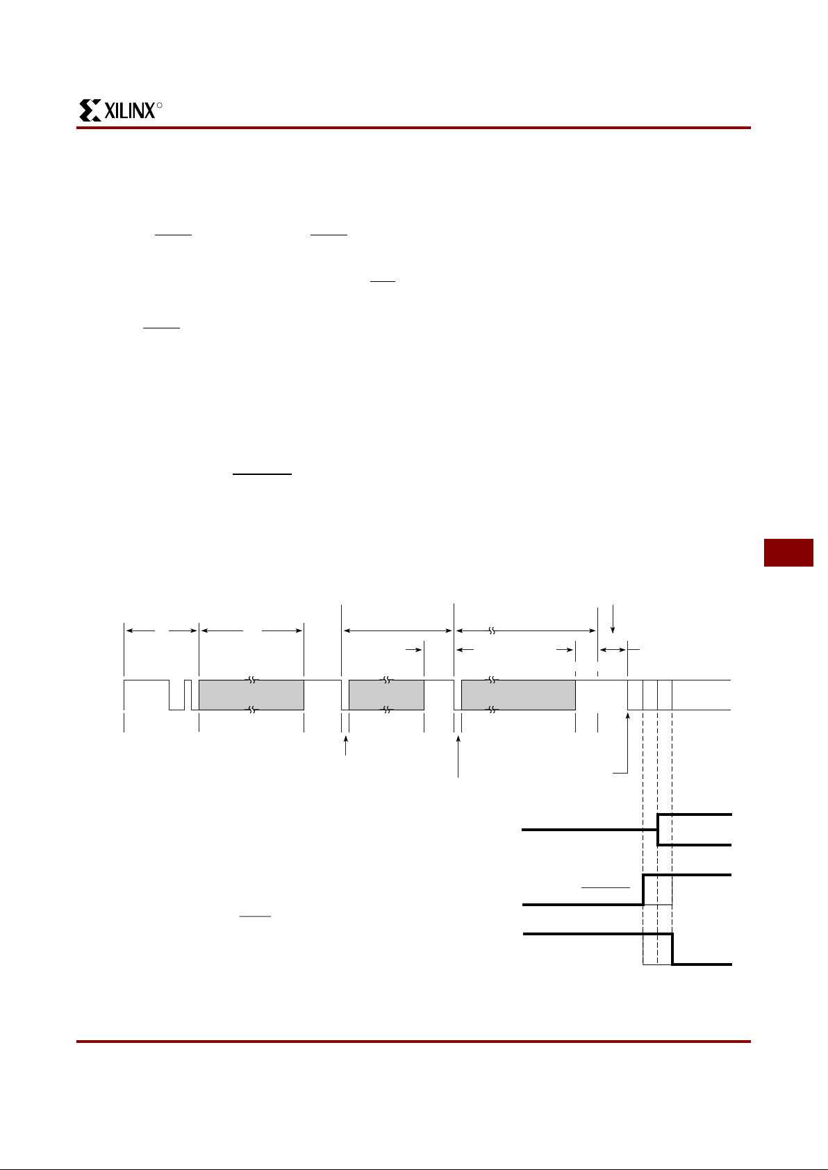
Timing of the assertion of DONE and
termination of the INTERNAL RESET
may each be programmed to occur
one cycle before or after the I/O outputs
become active.
Heavy lines indicate the default condition
X5988
PROGRAM
Weak Pull-Up
*
Stop
3
STOP
DIN
Figure 22: Configuration and Start-up of One or More FPGAs.

R
XC3000 Series Field Programmable Gate Arrays
7-22 November 9, 1998 (Version 3.1)
be used to drive the remaining unused routing, as that
might affect timing of user nets. Tie can be omitted for quick
breadboard iterat ions where a few additional millia mps of
Icc are acceptable.
The configuration bitstream begins with eight High pream-
ble bits, a 4-bit preamble code and a 24-bit length count.
When configuration is initiated, a counter in the FPGA is set
to zero and begins to count the total number of configura-
tion clock cycles ap plied to th e device . As each co nfigur a-
tion data frame is supplied to the device, it is internally
assembled into a data word, which is then loaded in parallel
into one word of th e internal configuration m emory array.
The configuration loading process is complete when the
current leng th cou nt equ als the load ed lengt h coun t and the
required configuration program data frames have been
written. In tern al us er f lip- flo ps a re he ld Re set during con fig -
uration.
Two user-programma ble pins are d efined in th e unconfig-
ured Field Progra mmab le Gate Ar ray. High During Config-
uration (HDC) and Low During Configuration (LDC
) as well
as DONE/PROG
may be used as external control signals
during configuration. In Master mode configurations it is
convenient to use LDC
as an active-Low EPROM Chip
Enable. After the last configuration data bit is loaded and
the length count compares, the user I/O pins become
active. Options allow timi ng choices o f one clock ear lier or
later for the timing of the end of the internal logic RESET
and the assertion of the DONE signal. The open-drain
DONE/PROG
output can be AND-tied with multiple devices
and used as an active -High REA DY, an active-Low PROM
enable or a RESET to other portions of the system. The
state diagram of Figure 20 illustrates the configuration pro-
cess.
Configuration Modes
Master Mode
In Master mode, the FPGA automatically loads configura-
tion data from an external memory device. There are three
Master modes that use the internal timing source to supply
the configuration clock (CCLK) to time the incoming data.
Master Serial mode uses serial configur ation data supplied
to Data-in (DIN) from a synch ron ous se rial so urce s uch as
the Xilinx Serial Configurat ion PROM shown in Figure 23.
Master Parallel Low and High modes automatically use
parallel data supplied to the D0–D7 pins in response to the
16-bit address generated by the FPGA. Figure 25 shows
an example of the parallel Master mode connections
required. T he HEX s tarting addres s is 0 000 and i ncreme nts
for Master Low mode and it is FFFF and decrements for
Master High mode. These two modes provide address
compatibility with microp rocessors which begin execution
from opposite ends of memory.
Peripheral Mode
Peripheral mode provides a simplified interface through
which the device may be loaded byte-wide, as a processor
peripheral. Figure 27 shows the peripheral mode connec-
tions. Processor write cycles are decoded from the com-
mon assertion of the active low Write Strobe (WS
), and two
active low and one active high Chip Selects (CS0
, CS1,
CS2). The FPGA generates a configuration clock from the
internal timing generator and serializes the parallel input
data for internal framing or for succeeding slaves on Data
Out (DOUT). A output High on READY/BUSY
pin indicates
the completion of loading for each byte when the input reg-
ister is ready for a n ew byte. As with Master modes, P eriph-
eral mode may also be used as a lead device for a
daisy-chain of slave devices.
Slave Serial Mode
Slave Serial mode provides a simple interface for loading
the Field Programmable Gate Array configuration as
shown in Figure29. Serial data is supplied in conjunction
with a synch ron izi n g i npu t cl oc k. M os t Sl av e m ode a ppli ca-
tions are in daisy-chain configurations in which the data
input is driven from the p revio us FP GA’s data out, w hile t he
clock is supplied by a lead device in Master or Peripheral
mode. Data may also be supplied by a processor or other
special circuits.
Daisy Chain
The development system is used to create a composite
configuration for selected FPGAs including: a preamble, a
length count for th e total bitstream, mu ltiple concatena ted
data programs a nd a postamble plus an ad ditional fill bit
per device in the serial chain. After loading and passing-on
the preamble and length count to a possible daisy-chain, a
lead device will load its configuration data frames while pro-
viding a High DOUT to possible down-stream devices as
shown in Figure 25. Loading continues while the lead
device has received its configuration program and the cur-
rent length count has not reached the full value. The addi-
tional data is passed through the lead device and appears
on the Data Out ( DOU T) p in i n s er ial f or m. T he le ad d ev ic e
also generates th e Confi gura tio n Clock (C CLK) t o synch ro-
nize the serial output data and data in of down-stream
FPGAs. Data is r ead in on DIN of sla ve devi ces by the po s-
itive edge of CCLK and shifted out the DOUT on the nega-
tive edge of CC LK. A p ar alle l M as te r mo de d ev ice use s it s
internal timing generator to produce an internal CCLK of 8
times its EPROM address rate, while a Peripheral mode
device produces a burst of 8 CCLKs for ea ch chip select
and write-strobe cycle. The internal timing generator con-
tinues to operate for general timing and synchronization of
inputs in all modes.
R
November 9, 1998 (Version 3.1) 7-23
XC3000 Series Field Programmable Gate Arrays
7
Special Configuration Functions
The configuration data includes control over several spe-
cial functions in addition to the normal user logic functions
and interconnect.
• Input thresholds
• Readback disabl e
• DONE pull-up resistor
•DONE timing
• RESET timing
• Oscillator frequen cy div ide d by tw o
Each of these functions is controlled by configuration data
bits which are selected as part of the normal development
system bitstream generation process.
Input Thresholds
Prior to the completion of configuration all FPGA input
thresholds are TTL compatible. Upon completion of config-
uration, the input thresholds become either TTL or CMOS
compatible as programmed. The use of the TTL threshold
option requires some additional supply current for thresh-
old shifting. The exception is the threshold of the
PWRDWN
input and direct clocks which always have a
CMOS input. Prior to the completion of configuration the
user I/O pins each have a high impedance pull-up. The
configuration program can be used to enable the IOB
pull-up resis tors in t he Op erat ional mode to act eit her a s an
input load or to avoid a floating input on an otherwise
unused pin.
Readback
The contents of a Fie ld Progr amm able Gat e Arr ay ma y be
read back if it has been programmed with a bitstream in
which the Readback option has been enabled. Readback
may be used for verification of configuration and as a
method of deter mining the st ate of inte rnal logic nodes dur -
ing debugging. There are three options in generating the
configuration bitstr ea m .
• “Never” inhibits the Read back capability.
• “One-time,” inhibits Readba ck after one Readback has
been executed to verify the configuration.
• “On-command ” allo ws unr es tric te d us e of Re ad ba ck .
Readback is acc omplished without the use of any of the
user I/O pins; only M0, M1 and CCLK are used. The initia-
tion of Readb ac k is pr odu ced by a Lo w to H i gh tr an si t io n o f
the M0/RTRIG (Read Trigger) pin. The CCLK input must
then be driven by ex t ernal l og ic t o re ad ba ck t he c onfi g ura -
tion data. The first three Low-to-High CCLK transitions
clock out dummy da ta. Th e subs equen t Low-t o-Hi gh CCLK
transitions shift the data frame information out on the
M1/RDATA
(Read Data) pin. No te that the logic polarity is
always inverted, a z ero in config uration beco mes a one in
Readback, and vice ver sa. Note also that eac h Readback
frame has one Start bit (read back as a one) but, unlike in
configuration, each Readback frame has only one Stop bit
(read back as a zero). The third leading dummy bit men-
tioned above can be considered the Start bit of the first
frame. All data fr ames mus t be read ba ck to comp lete the
process and retu rn the Mode Sel ect and CCL K pins t o thei r
normal functions.
Readback data includes the current state of each CLB
flip-flop, each input flip-flop or latch, and each device pad.
These data are imbedded into unused configuration bit
positions during Readback. This state information is used
by the development system In-Circuit Verifier to provide
visibility into the internal operation of the logic while the
system is operating. To read back a uniform time-sample of
all storage eleme nts , it may be nec essar y to in hibit the s ys-
tem clock.
Reprogram
To initiate a re-programming cycle, the dual-function pin
DONE/PROG
must be given a High-to-Low transition. To
reduce sensitivity to noise, the input signal is filtered for two
cycles of the FPGA internal timing generator. When repro-
gram begins, the us er-prog rammabl e I/O output buf fers are
disabled and high-impedance pull-ups are provided for the
package pins. The device returns to the Clear state and
clears the config uration memo ry before it ind icates ‘initial-
ized’. Since this Cle ar operatio n uses chip-in dividual inte r-
nal timing, the ma ster might co mplete the Cle ar operation
and then start conf igurati on before th e slave has com pleted
the Clear operation. To avoid this problem, the slave INIT
pins must be AND-wired and used to force a RESET on the
master (see Figure 25). Reprogram control is often imple-
mented using an external open-collector driver which pulls
DONE/PROG
Low. Once a stable request is recognized,
the DONE/PROG
pin is held Low until the new configura-
tion has been co mple te d. Even i f the r e- pro gr am r equ es t i s
externally held Low beyond the configuration period, the
FPGA will begin oper ation upon completion of config ura-
tion.
DONE Pull-up
DONE/PROG is an open-drain I/O pin that indicates the
FPGA is in the operational state. An optional internal
pull-up resistor can be enabled by the user of the develop-
ment system. The DONE/PROG
pins of multiple FPGAs in
a daisy-chain ma y be co nnect ed to geth er to ind ica te al l are
DONE or to direct them all to reprogram.
DONE Timing
The timing of the DONE status signal can be controlled by
a selection to occur either a CCLK cycle before, or after, the
outputs going active. See Figure 22. This facilitates control
of external functions such as a PROM enable or holding a
system in a wait state.
R
XC3000 Series Field Programmable Gate Arrays
7-24 November 9, 1998 (Version 3.1)
RESET Timing
As with DONE timing, the timing of the release of the inter-
nal reset can be controlled to occur either a CCLK cycle
before, or afte r, the outputs goi ng active. See Figure 22.
This reset keeps all user programmable flip-flops and
latches in a zero state durin g co nf igu ra tio n.
Crystal Oscillator Division
A selection allows the user to incorporate a dedicated
divide-by-two flip-flop between the crystal oscillator and the
alternate clock line. This guarantees a symmetrical clock
signal. Although the freque ncy stability of a c rystal osc illa-
tor is very good, the symmetry of its waveform can be
affected by bias or feedback drive.
Bitstream Error Checking
Bitstream error checking pr otects agai nst erroneous con-
figuration.
Each Xilinx FPGA bitst ream consis ts of a 40- bit pre amble,
followed by a device-specific number of data frames. The
number of bits pe r frame is als o device-spe cific; however,
each frame ends with three stop bits (111) followed by a
start bit for t he next frame (0).
All devices in all XC3000 fam ilies start reading in a new
frame when they f ind th e first 0 after th e end of t he prev ious
frame. An original XC3000 device does not check for the
correct stop bits, but XC3000A, XC3100A, XC3000L, and
XC3100L devic es che ck that the last t hree bit s of any fra me
are actually 111.
Under normal circumstances, all these FPGAs behave the
same way; however, if the bitstream is corrupted, an
XC3000 device will always sta rt a n ew fram e as so on as it
finds the first 0 after the end of the previous frame, even if
the data is completely wrong or out-of-sync. Given suffi-
cient zeros in the data stream, the device will also go Done,
but with incorre ct config uration an d the possib ility of inte r-
nal contention.
An XC3000A/XC3100A/XC3000L/XC3100L device starts
any new frame only if the three preceding bits are all ones.
If this check fails, it pulls INIT
Low and stops the int ernal
configuration, although the Master CCLK keeps running.
The user must then start a new configuration by applying a
>6 µs Low level on RESET
.
This simple check does not protect against random bit
errors, but it offers almost 100 percent protection against
erroneous configuration files, defective configuration data
sources, synchronization errors between configuration
source and FPGA, or PC-board level defects, such as bro-
ken lines or solder-bridges.
Reset Spike Protection
A separate modification slows down the RESET input
before configuration by using a two-stage shift register
driven from the in ternal cloc k. It tolerates s ubmicrose cond
High spikes on RESET
before configur ation. The X C3000
master can be connected like an XC4000 master, but with
its RESET
input used instead of INIT. (On XC3000, INIT is
output only).
Soft Start-up
After configuration, the outputs of all FPGAs in a
daisy-chain become active simultaneously, as a result of
the same CCLK edge. In the original XC3000/3100
devices, each output becomes active in either fast or
slew-rate limited mode, depending on the way it is config-
ured. This can lead to large ground-bounce signals. In
XC3000A, XC3000L, XC3100A, and XC3100L devices, all
outputs become active first in slew-rate limited mode,
reducing the ground bounce. After this soft start-up, each
individual output slew rate is again controlled by the
respective configuration bit.
R
November 9, 1998 (Version 3.1) 7-25
XC3000 Series Field Programmable Gate Arrays
7
Configuration Timing
This section describes the configuration modes in detail.
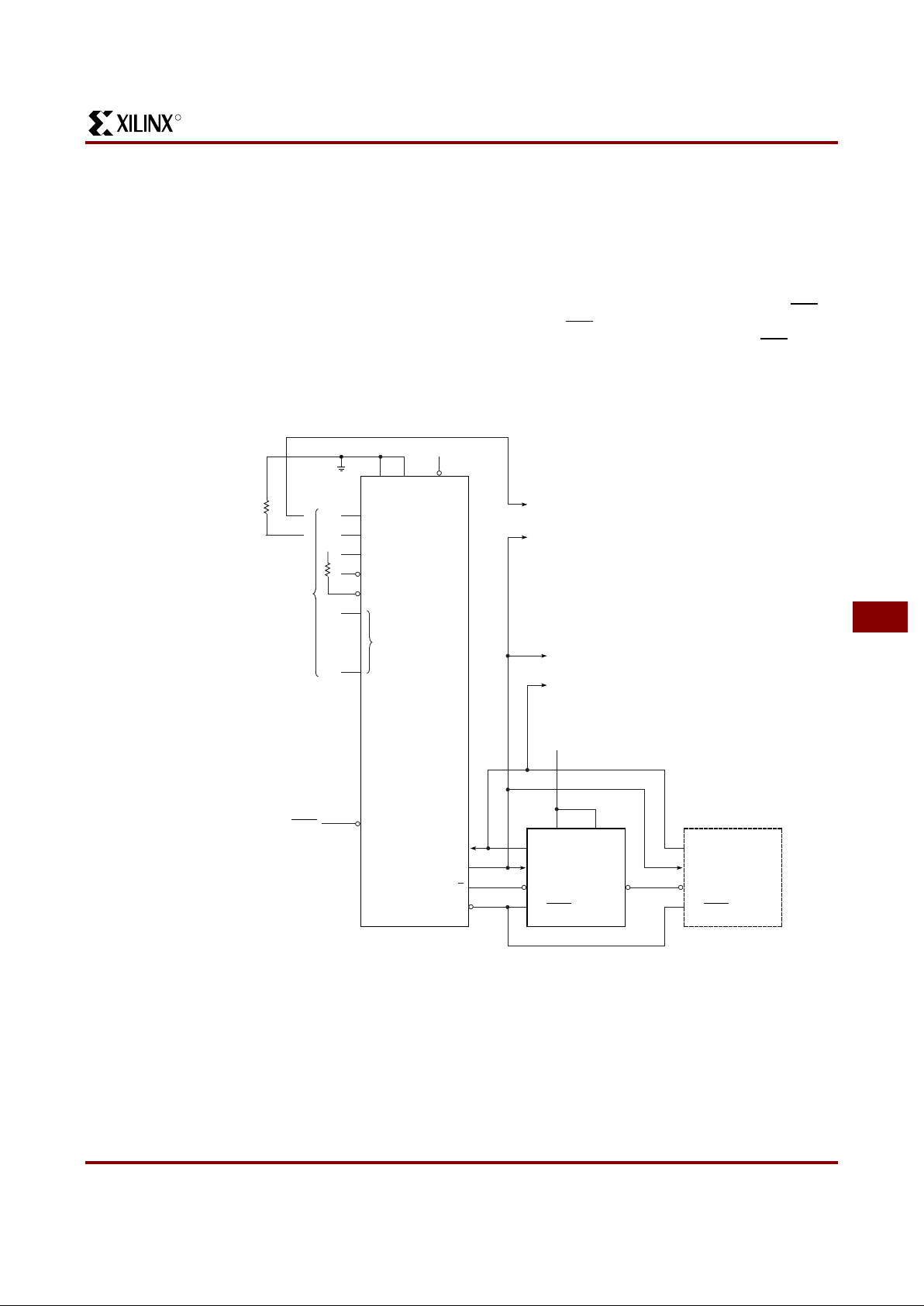
Master Serial Mode
In Master Serial mode, the CCLK output of the lead FPGA
drives a Xilinx Serial PROM that feeds the DIN input. Each
rising edge of the CCLK output increments the Serial
PROM internal address counter. This puts the next data bit
on the SPROM data output, connected to the DIN pin. The
lead FPGA accepts this data on the subsequent rising
CCLK edge.
The lead FPGA then presents the preamble data (and all
data that over flows t he lead dev ice) on its DOUT p in. There
is an internal delay of 1.5 CCLK periods, which means that
DOUT changes on the falling CCLK edge, and the next
device in the daisy-chain accepts data on the subsequent
rising CCLK edge.
The SPROM CE input can be driven f rom either LDC
or
DONE. Using LDC
avoids potential contention on the DIN
pin, if this pin is configured as user-I/ O, but LDC
is then
restricted to be a permanently High user output. Using
DONE also avoids contention on DIN, provided the early
DONE option is invoked.
X5989_01
CE
GENERAL-
PURPOSE
USER I/O
PINS
M0 M1 PWRDWN
DOUT
M2
HDC
OTHER
I/O PINS
RESET
DIN
CCLK
DATA
CLK
+5 V
•
•
•
•
•
OE/RESET
XC3000
FPGA
DEVICE
D/P
SCP
CEO
CASCADED
SERIAL
MEMORY
LDC
INIT
XC17xx
RESET
SLAVE LCAs WITH IDENTICAL
CONFIGURATIONS
DURING CONFIGURATION
THE 5 kΩ M2 PULL-DOWN
RESISTOR OVERCOMES THE
INTERNAL PULL-UP,
BUT IT ALLOWS M2 TO
BE USER I/O.
(LOW RESETS THE XC17xx ADDRESS POINTER)
TO CCLK OF OPTIONAL
V
CC
V
PP
+5 V
DAISY-CHAINED LCAs WITH
DIFFERENT CONFIGURATIONS
TO DIN OF OPTIONAL
IF READBACK IS
ACTIVATED, A
5-kΩ RESISTOR IS
REQUIRED IN
SERIES WITH M1
*
*
CE
DATA
CLK
OE/RESET
DAISY-CHAINED LCAs WITH
DIFFERENT CONFIGURATIONS
TO CCLK OF OPTIONAL
SLAVE LCAs WITH IDENTICAL
CONFIGURATIONS
TO DIN OF OPTIONAL
INIT
+5V
Figure 23: Master Serial Mode Circuit Diagram
 Loading...