


XILINX XC1765EPC20C, XC1765ELVO8I, XC1765ELVO8C, XC1765ELSO8I, XC1765ELPD8I Datasheet
...
R
XC1700E and XC1700L Series
Configuration PROMs
DS027 (v3.1) July 5, 2000 |
Product Specification |
Features
•One-time programmable (OTP) read-only memory designed to store configuration bitstreams of Xilinx FPGA devices
•Simple interface to the FPGA; requires only one user I/O pin
•Cascadable for storing longer or multiple bitstreams
•Programmable reset polarity (active High or active Low) for compatibility with different FPGA solutions
•XC17128E/EL, XC17256E/EL, XC1701 and XC1700L series support fast configuration
•Low-power CMOS Floating Gate process
•XC1700E series are available in 5V and 3.3V versions
•XC1700L series are available in 3.3V only
•Available in compact plastic packages: 8-pin SOIC, 8-pin VOIC, 8-pin PDIP, 20-pin SOIC, 20-pin PLCC, 44-pin PLCC or 44-pin VQFP.
•Programming support by leading programmer manufacturers.
•Design support using the Xilinx Alliance and Foundation series software packages.
•Guaranteed 20 year life data retention
Description
The XC1700 family of configuration PROMs provides an easy-to-use, cost-effective method for storing large Xilinx FPGA configuration bitstreams.
When the FPGA is in Master Serial mode, it generates a configuration clock that drives the PROM. A short access time after the rising clock edge, data appears on the PROM DATA output pin that is connected to the FPGA DIN pin. The FPGA generates the appropriate number of clock pulses to complete the configuration. Once configured, it disables the PROM. When the FPGA is in Slave Serial mode, the PROM and the FPGA must both be clocked by an incoming signal.
Multiple devices can be concatenated by using the CEO output to drive the CE input of the following device. The clock inputs and the DATA outputs of all PROMs in this chain are interconnected. All devices are compatible and can be cascaded with other members of the family.
For device programming, either the Xilinx Alliance or Foundation series development system compiles the FPGA design file into a standard Hex format, which is then transferred to most commercial PROM programmers.
|
VCC |
VPP |
GND |
|
|
RESET/ |
CE |
|
|
|
CEO |
OE |
|
|
|
||
|
|
|
|
|
|
or |
|
|
|
|
|
OE/ |
|
|
|
|
|
RESET |
|
|
|
|
|
|
CLK |
|
Address Counter |
TC |
|
|
|
|
|
||
|
|
|
EPROM |
Output |
OE |
|
|
|
Cell |
DATA |
|
|
|
|
|
||
|
|
|
Matrix |
|
|
|
|
|
|
|
DS027_01_021500 |
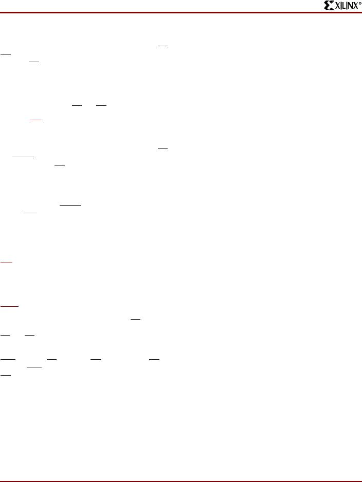
Figure 1: Simplified Block Diagram (does not show programming circuit)
© 2000 Xilinx, Inc. All rights reserved. All Xilinx trademarks, registered trademarks, patents, and disclaimers are as listed at http://www.xilinx.com/legal.htm. All other trademarks and registered trademarks are the property of their respective owners. All specifications are subject to change without notice.
DS027 (v3.1) July 5, 2000 |
www.xilinx.com |
1 |
Product Specification |
1-800-255-7778 |
|
XC1700E and XC1700L Series Configuration PROMs
R
Pin Description
DATA
Data output is in a high-impedance state when either CE or
OE are inactive. During programming, the DATA pin is I/O. Note that OE can be programmed to be either active High or active Low.
CLK
Each rising edge on the CLK input increments the internal address counter, if both CE and OE are active.
VPP
Programming voltage. No overshoot above the specified max voltage is permitted on this pin. For normal read operation, this pin must be connected to VCC. Failure to do so may lead to unpredictable, temperature-dependent operation and severe problems in circuit debugging. Do not leave VPP floating!
VCC and GND
Positive supply and ground pins.
RESET/OE
When High, this input holds the address counter reset and puts the DATA output in a high-impedance state. The polarity of this input pin is programmable as either RESET/OE or OE/RESET. To avoid confusion, this document describes the pin as RESET/OE, although the opposite polarity is possible on all devices. When RESET is active, the address counter is held at "0", and puts the DATA output in a high-impedance state. The polarity of this input is programmable. The default is active High RESET, but the preferred option is active Low RESET, because it can be driven by the FPGAs INIT pin.
The polarity of this pin is controlled in the programmer interface. This input pin is easily inverted using the Xilinx HW-130 Programmer. Third-party programmers have different methods to invert this pin.
CE
When High, this pin disables the internal address counter, puts the DATA output in a high-impedance state, and forces the device into low-ICC standby mode.
CEO
Chip Enable output, to be connected to the CE input of the next PROM in the daisy chain. This output is Low when the CE and OE inputs are both active AND the internal address counter has been incremented beyond its Terminal Count (TC) value. In other words: when the PROM has been read, CEO will follow CE as long as OE is active. When OE goes inactive, CEO stays High until the PROM is reset. Note that OE can be programmed to be either active High or active Low.
PROM Pinouts
|
|
|
|
|
|
|
|
8-pin |
|
|
|
|
|
|
|
|
|
|
|
|
|
|
|
PDIP |
|
|
|
|
|
|
|
|
|
|
|
|
|
|
|
SOIC |
20-pin |
20-pin |
44-pin |
44-pin |
|||
|
Pin Name |
|
VOIC |
SOIC |
PLCC |
|
VQFP |
PLCC |
|||||||
|
|
|
|
|
|
|
|
|
|
|
|||||
|
DATA |
|
1 |
|
1 |
2 |
|
40 |
2 |
|
|||||
|
|
|
|
|
|
|
|
|
|
|
|||||
|
CLK |
|
2 |
|
3 |
4 |
|
43 |
5 |
|
|||||
|
|
|
|
|
|
|
|
|
|
|
|
|
|
|
|
|
|
|
|
|
|
|
|
3 |
|
8 |
6 |
|
13 |
19 |
|
|
RESET/OE |
|
|
|
|
|
|||||||||
|
|
|
|
|
|
|
|
|
|
|
|
|
|
||
|
(OE/RESET) |
|
|
|
|
|
|
|
|
||||||
|
|
|
|
|
|
|
|
|
|
|
|
|
|||
|
|
|
|
|
4 |
|
10 |
8 |
|
15 |
21 |
||||
|
CE |
||||||||||||||
|
|
|
|
|
|
|
|
|
|
|
|||||
|
GND |
|
5 |
|
11 |
10 |
|
18, 41 |
24, 3 |
||||||
|
|
|
|
|
|
|
|
|
|
|
|
||||
|
|
|
|
|
6 |
|
13 |
14 |
|
21 |
27 |
||||
|
CEO |
||||||||||||||
|
|
|
|
|
|
|
|
|
|
|
|||||
|
VPP |
|
7 |
|
18 |
17 |
|
35 |
41 |
||||||
|
VCC |
|
8 |
|
20 |
20 |
|
38 |
44 |
||||||
Capacity |
|
|
|
|
|
|
|
|
|||||||
|
|
|
|
|
|
|
|
|
|||||||
|
|
|
Devices |
|
|
Configuration Bits |
|
|
|||||||
|
|
|
|
|
|
|
|
|
|
||||||
|
|
|
XC1704L |
|
|
|
4,194,304 |
|
|
||||||
|
|
|
|
|
|
|
|
|
|
||||||
|
|
|
XC1702L |
|
|
|
2,097,152 |
|
|
||||||
|
|
|
|
|
|
|
|
|
|||||||
|
|
XC1701/L |
|
|
|
1,048,576 |
|
|
|||||||
|
|
|
|
|
|
|
|
|
|||||||
|
|
XC17512L |
|
|
|
524,288 |
|
|
|||||||
|
|
|
|
|
|
|
|
|
|
|
|||||
|
|
|
XC1736E |
|
|
|
36,288 |
|
|
|
|||||
|
|
|
|
|
|
|
|
||||||||
|
XC1765E/EL |
|
|
65,536 |
|
|
|
||||||||
|
|
|
|
|
|
|
|||||||||
|
XC17128E/EL |
|
|
131,072 |
|
|
|||||||||
|
|
|
|
|
|
|
|||||||||
|
XC17256E/EL |
|
|
262,144 |
|
|
|||||||||
|
|
|
|
|
|
|
|
|
|
|
|
|
|
|
|
2 |
www.xilinx.com |
DS027 (v3.1) July 5, 2000 |
|
1-800-255-7778 |
Product Specification |

R
XC1700E and XC1700L Series Configuration PROMs
Xilinx FPGAs and Compatible PROMs
|
Configuration |
|
Device |
Bits |
PROM |
|
|
|
XC4003E |
53,984 |
XC17128E(1) |
XC4005E |
95,008 |
XC17128E |
|
|
|
XC4006E |
119,840 |
XC17128E |
|
|
|
XC4008E |
147,552 |
XC17256E |
|
|
|
XC4010E |
178,144 |
XC17256E |
|
|
|
XC4013E |
247,968 |
XC17256E |
|
|
|
XC4020E |
329,312 |
XC1701 |
|
|
|
XC4025E |
422,176 |
XC1701 |
|
|
|
XC4002XL |
61,100 |
XC17128EL(1) |
XC4005XL |
151,960 |
XC17256EL |
|
|
|
XC4010XL |
283,424 |
XC17512L |
|
|
|
XC4013XL/XLA |
393,632 |
XC17512L |
|
|
|
XC4020XL/XLA |
521,880 |
XC17512L |
|
|
|
XC4028XL/XLA |
668,184 |
XC1701L |
|
|
|
XC4028EX |
668,184 |
XC1701 |
|
|
|
XC4036EX/XL/XLA |
832,528 |
XC1701L |
|
|
|
XC4036EX |
832,528 |
XC1701 |
|
|
|
XC4044XL/XLA |
1,014,928 |
XC1701L |
|
|
|
XC4052XL/XLA |
1,215,368 |
XC1702L |
|
|
|
XC4062XL/XLA |
1,433,864 |
XC1702L |
|
|
|
XC4085XL/XLA |
1,924,992 |
XC1702L |
|
|
|
XC40110XV |
2,686,136 |
XC1704L |
|
|
|
XC40150XV |
3,373,448 |
XC1704L |
|
|
|
XC40200XV |
4,551,056 |
XC1704L + |
|
|
XC17512L |
|
|
|
XC40250XV |
5,433,888 |
XC1704L+ |
|
|
XC1702L |
|
|
|
XC5202 |
42,416 |
XC1765E |
|
|
|
XC5204 |
70,704 |
XC17128E |
|
|
|
|
Configuration |
|
Device |
Bits |
PROM |
|
|
|
XC5206 |
106,288 |
XC17128E |
|
|
|
XC5210 |
165,488 |
XC17256E |
|
|
|
XC5215 |
237,744 |
XC17256E |
|
|
|
XCV50 |
559,232 |
XC1701L |
|
|
|
XCV100 |
781,248 |
XC1701L |
|
|
|
XCV150 |
1,041,128 |
XC1701L |
|
|
|
XCV200 |
1,335,872 |
XC1702L |
|
|
|
XCV300 |
1,751,840 |
XC1702L |
|
|
|
XCV400 |
2,546,080 |
XC1704L |
|
|
|
XCV600 |
3,608,000 |
XC1704L |
|
|
|
XCV800 |
4,715,648 |
XC1704L + |
|
|
XC1701L |
|
|
|
XCV1000 |
6,127,776 |
XC1704L + |
|
|
XC1702L |
|
|
|
XCV50E |
630,048 |
XC1701L |
|
|
|
XCV100E |
863,840 |
XC1701L |
|
|
|
XCV200E |
1,442,106 |
XC1702L |
|
|
|
XCV300E |
1,875,648 |
XC1702L |
|
|
|
XCV400E |
2,693,440 |
XC1704L |
|
|
|
XCV405E |
3,340,400 |
XC1704L |
|
|
|
XCV600E |
3,961,632 |
XC1704L |
|
|
|
XCV812E |
6,519,648 |
2 of XC1704L |
|
|
|
XCV1000E |
6,587,520 |
2 of XC1704L |
|
|
|
XCV1600E |
8,308,992 |
2 of XC1704L |
|
|
|
XCV2000E |
10,159,648 |
3 of XC1704L |
|
|
|
XCV2600E |
12,922,336 |
4 of XC1704L |
|
|
|
XCV3200E |
16,283,712 |
4 of XC1704L |
|
|
|
Notes:
1.The suggested PROM is determined by compatibility with the higher configuration frequency of the Xilinx FPGA CCLK. Designers using the default slow configuration frequency (CCLK) can use the XC1765E or XC1765EL for the noted FPGA devices.
DS027 (v3.1) July 5, 2000 |
www.xilinx.com |
3 |
Product Specification |
1-800-255-7778 |
|
XC1700E and XC1700L Series Configuration PROMs
R
Controlling PROMs
Connecting the FPGA device with the PROM.
•The DATA output(s) of the of the PROM(s) drives the DIN input of the lead FPGA device.
•The Master FPGA CCLK output drives the CLK input(s) of the PROM(s).
•The CEO output of a PROM drives the CE input of the next PROM in a daisy chain (if any).
•The RESET/OE input of all PROMs is best driven by the INIT output of the lead FPGA device. This connection assures that the PROM address counter is reset before the start of any (re)configuration, even when a reconfiguration is initiated by a VCC glitch. Other methods—such as driving RESET/OE from LDC or system reset—assume the PROM internal power-on-reset is always in step with the FPGA’s internal power-on-reset. This may not be a safe assumption.
•The PROM CE input can be driven from either the LDC or DONE pins. Using LDC avoids potential contention on the DIN pin.
•The CE input of the lead (or only) PROM is driven by the DONE output of the lead FPGA device, provided that DONE is not permanently grounded. Otherwise, LDC can be used to drive CE, but must then be unconditionally High during user operation. CE can also be permanently tied Low, but this keeps the DATA output active and causes an unnecessary supply current of 10 mA maximum.
FPGA Master Serial Mode Summary
The I/O and logic functions of the Configurable Logic Block (CLB) and their associated interconnections are established by a configuration program. The program is loaded either automatically upon power up, or on command, depending on the state of the three FPGA mode pins. In Master Serial mode, the FPGA automatically loads the configuration program from an external memory. The Xilinx PROMs have been designed for compatibility with the Master Serial mode.
Upon power-up or reconfiguration, an FPGA enters the Master Serial mode whenever all three of the FPGA mode-select pins are Low (M0=0, M1=0, M2=0). Data is read from the PROM sequentially on a single data line. Synchronization is provided by the rising edge of the temporary signal CCLK, which is generated during configuration.
Master Serial Mode provides a simple configuration interface. Only a serial data line and two control lines are required to configure an FPGA. Data from the PROM is
read sequentially, accessed via the internal address and bit counters which are incremented on every valid rising edge of CCLK.
If the user-programmable, dual-function DIN pin on the FPGA is used only for configuration, it must still be held at a defined level during normal operation. The Xilinx FPGA families take care of this automatically with an on-chip default pull-up resistor.
Programming the FPGA With Counters
Unchanged Upon Completion
When multiple FPGA-configurations for a single FPGA are stored in a PROM, the OE pin should be tied Low. Upon power-up, the internal address counters are reset and configuration begins with the first program stored in memory. Since the OE pin is held Low, the address counters are left unchanged after configuration is complete. Therefore, to reprogram the FPGA with another program, the DONE line is pulled Low and configuration begins at the last value of the address counters.
This method fails if a user applies RESET during the FPGA configuration process. The FPGA aborts the configuration and then restarts a new configuration, as intended, but the PROM does not reset its address counter, since it never saw a High level on its OE input. The new configuration, therefore, reads the remaining data in the PROM and interprets it as preamble, length count etc. Since the FPGA is the master, it issues the necessary number of CCLK pulses, up to 16 million (224) and DONE goes High. However, the FPGA configuration will be completely wrong, with potential contentions inside the FPGA and on its output pins. This method must, therefore, never be used when there is any chance of external reset during configuration.
Cascading Configuration PROMs
For multiple FPGAs configured as a daisy-chain, or for future FPGAs requiring larger configuration memories, cascaded PROMs provide additional memory. After the last bit from the first PROM is read, the next clock signal to the PROM asserts its CEO output Low and disables its DATA line. The second PROM recognizes the Low level on its CE input and enables its DATA output. See Figure 2.
After configuration is complete, the address counters of all cascaded PROMs are reset if the FPGA RESET pin goes Low, assuming the PROM reset polarity option has been inverted.
To reprogram the FPGA with another program, the DONE line goes Low and configuration begins where the address counters had stopped. In this case, avoid contention between DATA and the configured I/O use of DIN.
4 |
www.xilinx.com |
DS027 (v3.1) July 5, 2000 |
|
1-800-255-7778 |
Product Specification |
 Loading...