


XICOR XM28C040MHR-25, XM28C040MHR-20, XM28C040MHR, XM28C040M-25, XM28C040M-20 Datasheet
...
XM28C040
4 Megabit Module |
XM28C040 |
512K x 8 Bit |
5 Volt, Byte Alterable E2PROM
TYPICAL FEATURES
•High Density 4 Megabit (512K x 8) Module
•Access Time of 200ns at –55°C to +125°C
•Base Memory Component: Xicor X28C010
•Pinout Conforms to JEDEC Standard for 4 Megabit E2PROM
•Fast Write Cycle Times —256 Byte Page Write
•Early End of Write Detection
— DATA Polling
—Toggle Bit Polling
•Software Data Protection
•Three Temperature Ranges —Commercial: 0 °C to +75°C —Industrial: –40 ° to +85°C —Military: –55 ° to +125°C
•High Rel Modules all Components are MIL-STD-883 Compliant
•Endurance: 100,000 Cycles
DESCRIPTION
The XM28C040 is a high density 4 Megabit E2PROM comprised of four X28C010's mounted on a co-fired multilayered ceramic substrate. Individual components are 100% tested prior to assembly in module form and then 100% tested after assembly.
The XM28C040 is configured 512K x 8 bit. The module supports a 256-byte page write operation. This combined with DATA Polling or Toggle Bit Polling, effectively provides a 39μs/byte write cycle, enabling the entire array to be rewritten in 10 seconds.
The XM28C040 provides the same high endurance and data retention as the X28C010.
FUNCTIONAL DIAGRAM |
|
|
|
X28C010 |
X28C010 |
|
A0–A16 |
A0–A16 |
|
I/O0–I/O7 |
I/O0–I/O7 |
|
OE |
OE |
|
WE |
WE |
|
CE |
CE |
|
X28C010 |
X28C010 |
A0–A16 |
A0–A16 |
A0–A16 |
I/O0–I/O7 |
I/O0–I/O7 |
I/O0–I/O7 |
OE |
OE |
OE |
WE |
WE |
WE |
CE |
CE |
CE |
A18 |
|
|
A17 |
|
|
PIN CONFIGURATION
A18 |
|
1 |
|
|
32 |
|
VCC |
||||
|
|
|
|
||||||||
|
|||||||||||
A16 |
|
2 |
|
|
31 |
|
|
WE |
|
||
|
|||||||||||
A15 |
|
3 |
|
|
30 |
|
A17 |
||||
|
|||||||||||
A12 |
|
4 |
|
|
29 |
|
A14 |
||||
|
|||||||||||
A7 |
|
5 |
|
|
28 |
|
A13 |
||||
|
|||||||||||
A6 |
|
6 |
|
|
27 |
|
A8 |
||||
|
|||||||||||
A5 |
|
7 |
|
|
26 |
|
A9 |
||||
|
|||||||||||
A4 |
|
8 |
|
|
25 |
|
A11 |
||||
|
|||||||||||
|
|
XM28C040 |
|
|
|
|
|
|
|
||
A3 |
|
9 |
|
|
24 |
|
|
OE |
|
||
|
|||||||||||
A2 |
|
10 |
|
|
23 |
|
A10 |
||||
|
|||||||||||
A1 |
|
11 |
|
|
22 |
|
|
CE |
|
||
|
|
|
|
||||||||
A0 |
|
12 |
|
|
21 |
|
I/O7 |
||||
|
|
|
|
||||||||
I/O0 |
|
13 |
|
|
20 |
|
I/O6 |
||||
|
|
|
|
||||||||
I/O1 |
|
14 |
|
|
19 |
|
I/O5 |
||||
|
|
|
|
||||||||
I/O2 |
|
15 |
|
|
18 |
|
I/04 |
||||
|
|||||||||||
VSS |
|
16 |
|
|
17 |
|
I/O3 |
||||
|
|||||||||||
3873 FHD F02
|
3873 FHD F01 |
|
|
|
|
© Xicor, Inc. 1991-1997 Patents Pending |
1 |
Characteristics subject to change without notice |
3873-1.7 6/13/97 T1/C0/D0 SH |
|
|
|
|

XM28C040
PIN DESCRIPTIONS
Addresses (A –A )
0 18
The Address inputs select an 8-bit memory location during a read or write operation.
Chip Enable (CE)
The Chip Enable input must be LOW to enable all read/ write operations. When CE is HIGH, power consumption is reduced (see Note 4).
Output Enable (OE)
The Output Enable input controls the data output buffers and is used to initiate read operations.
Data In/Data Out (I/O –I/O)
0 7
Data is written to or read from the XM28C040 through the I/O pins.
Write Enable (WE)
The Write Enable input controls the writing of data to the XM28C040.
PIN NAMES
Symbol |
Description |
|
|
A0–A18 |
Address Inputs |
I/O0–I/O8 |
Data Input/Output |
WE |
Write Enable |
|
|
CE |
Chip Enable |
OE |
Output Enable |
|
|
VCC |
+5V |
VSS |
Ground |
NC |
No Connect |
|
|
3873 PGM T01
2

XM28C040
DEVICE OPERATION
Read
Read operations are initiated by both OE and CE LOW. The read operation is terminated by either CE or OE returning HIGH. This 2-line control architecture eliminates bus contention in a system environment. The data bus will be in a high impedance state when either OE or CE is HIGH.
Write
Write operations are initiated when both CE and WE are LOW and OE is HIGH. The XM28C040 supports both a CE and WE controlled write cycle. That is, the address is latched by the falling edge of either CE or WE, whichever occurs last. Similarly, the data is latched internally by the rising edge of either CE or WE, whichever occurs first. A byte write operation, once initiated, will automatically continue to completion, typically within 5ms (see Note 4).
Page Write Operation
The page write feature of the XM28C040 allows the entire memory to be written in 10 seconds. Page write allows two to 256 bytes of data to be consecutively written to the XM28C040 prior to the commencement of the internal programming cycle. The host can fetch data from another device within the system during a page write operation (change the source address), but the page address (A8 through A18) for each subsequent valid write cycle to the part during this operation must be the same as the initial page address.
The page write mode can be initiated during any write operation. Following the initial byte write cycle, the host can write an additional one to 255 bytes in the same manner as the first byte was written. Each successive byte load cycle, started by the WE HIGH to LOW transition, must begin within 100μs of the falling edge of the preceding WE. If a subsequent WE HIGH to LOW transition is not detected within 100μs, the internal automatic programming cycle will commence. There is no page write window limitation. Effectively the page write window is infinitely wide, so long as the host
continues to access the device within the byte load cycle time of 100μs.
Write Operation Status Bits
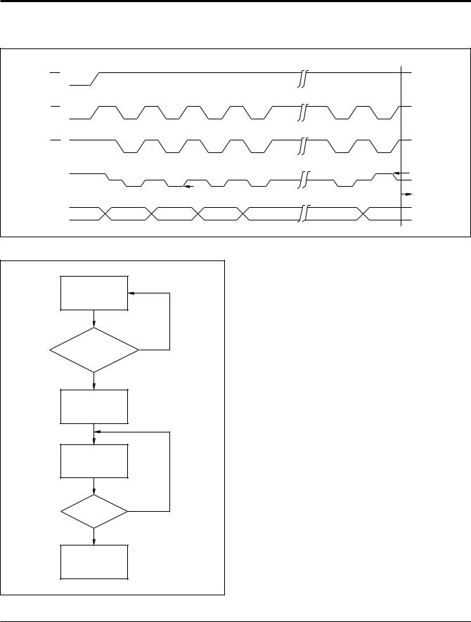
The XM28C040 provides the user two write operation status bits. These can be used to optimize a system write cycle time. The status bits are mapped onto the I/O bus as shown in Figure 1.
DATA Polling (I/O7)
Figure 1. Status Bit Assignment
I/O |
DP |
TB |
5 |
4 |
3 |
2 |
1 |
0 |
|
|
|
|
|
|
|
|
|
RESERVED
TOGGLE BIT
DATA POLLING
3873 FHD F09
The XM28C040 features DATA Polling as a method to indicate to the host system that the byte write or page write cycle has completed. DATA Polling allows a simple bit test operation to determine the status of the XM28C040, eliminating additional interrupt inputs or external hardware. During the internal programming cycle, any attempt to read the last byte written will produce the complement of that data on I/O7 (i.e., write data = 0xxx xxxx, read data = 1xxx xxxx). Once the programming cycle is complete, I/O7 will reflect true data. Note: If the XM28C040 is in the protected state and an illegal write operation is attempted, DATA Polling will not operate.
Toggle Bit (I/O6)
The XM28C040 also provides another method for determining when the internal write cycle is complete. During the internal programming cycle I/O6 will toggle from “1” to “0” and “0” to “1” on subsequent attempts to read the last byte written. When the internal cycle is complete the toggling will cease and the device will be accessible for additional read or write operations.
3
XM28C040
DATA POLLING I/O7
Figure 2. DATA Polling Bus Sequence
|
LAST |
|
|
|
|
|
|
|
WE |
WRITE |
|
|
|
|
|
|
|
CE |
|
|
|
|
|
|
|
|
OE |
|
|
|
|
|
|
|
|
|
VIH |
|
HIGH Z |
|
|
|
V |
OH |
I/O7 |
|
|
|
|
|
|||
|
|
|
VOL |
|
|
|
||
|
|
|
|
|
|
READY |
||
|
|
|
|
|
|
|
||
A0–A18 |
An |
An |
An |
An |
An |
An |
An |
|
|
|
|
|
|
|
|
|
3873 FHD F10 |
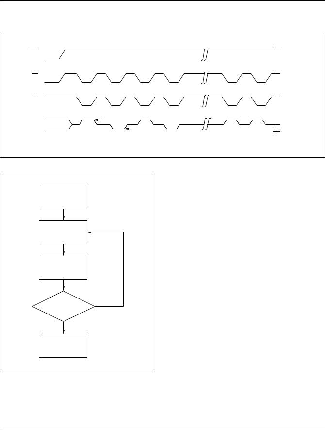
Figure 3. DATA Polling Software Flow
WRITE DATA
WRITES NO
COMPLETE?
YES
SAVE LAST DATA
AND ADDRESS
READ LAST |
|
ADDRESS |
|
IO7 |
NO |
COMPARE? |
|
YES |
|
READY |
|
DATA Polling can effectively halve the time for writing to the XM28C040. The timing diagram in Figure 2 illustrates the sequence of events on the bus. The software flow diagram in Figure 3 illustrates one method of implementing the routine.
3873 FHD F11
4
XM28C040
THE TOGGLE BIT I/O6
Figure 4. Toggle Bit Bus Sequence
LAST
WE WRITE
CE |
|
|
|
OE |
|
|
|
I/O6 |
* |
VOH |
HIGH Z |
VOL |
* |
||
|
|
READY |
* Beginning and ending state of I/O6 will vary.
3873 FHD F12
Figure 5. Toggle Bit Software Flow
LAST WRITE
LOAD ACCUM
FROM ADDR n
COMPARE
ACCUM WITH
ADDR n
NO
COMPARE
OK?
YES
The Toggle Bit can eliminate the software housekeeping chore of saving and fetching the last address and data written to a device in order to implement DATA Polling. This can be especially helpful in an array comprised of multiple XM28C040 memories that is frequently updated. The timing diagram in Figure 4 illustrates the sequence of events on the bus. The software flow diagram in Figure 5 illustrates a method for testing the Toggle Bit.
READY
3873 FHD F13
5

XM28C040
HARDWARE DATA PROTECTION
The XM28C040 provides three hardware features that protect nonvolatile data from inadvertent writes.
•Noise Protection—A WE pulse less than 10ns will not initiate a write cycle.
•Default VCC Sense—All functions are inhibited when VCC is ≤ 3V.
•Write Inhibit—Holding OE LOW will prevent an inadvertent write cycle during power-up and power-down.
SOFTWARE DATA PROTECTION
The XM28C040 does provide the Software Data Protection (SDP) feature.
The module is shipped from Xicor with the Software Data Protection NOT ENABLED; that is, the module will be in the standard operating mode. In this mode, data should be protected during power-up/-down operations through the use of external circuits. The host system will then have open read and write access of the module once VCC is stable.
The module can be automatically protected during power- up/-down without the need for external circuits by employing the SDP feature. The internal SDP circuit is enabled after the first write operation utilizing the SDP command sequence.
When this feature is employed, it will be easiest to incorporate in the system software if the module is viewed as a subsystem composed of four discrete memory devices with an address decoder (see Functional Diagram). In this manner, system memory mapping will extend onto the module. That is, the discrete
memory ICs and decoder should be considered memory board components and SDP can be implemented at the component level as described in the next section.
SOFTWARE COMMAND SEQUENCE
A17 and A18 are used by the decoder to select one of the four LCCs. Therefore, only one of the four memory devices can be accessed at one time. In order to protect the entire module, the command sequence must be issued separately to each device.
Enabling the software data protection mode requires the host system to issue a series of three write operations: each write operation must conform to the data and address sequence illustrated in Figures 6 and 7. Because this involves writing to a nonvolatile bit, the device will become protected after tWC has elapsed. After this point in time devices will inhibit inadvertent write operations.
Once in the protected mode, authorized writes may be performed by issuing the same command sequence that enables SDP, immediately followed by the address/data combination desired. The command sequence opens the page write window enabling the host to write from one to 256 bytes of data. Once the data has been written, the device will automatically be returned to the protected state.
In order to facilitate testing of the devices the SDP mode can be deactivated. This is accomplished by issuing a series of six write operations: each write operation must conform to the data and address sequence illustrated in Figures 8 and 9. This is a nonvolatile operation, and the host will have to wait a minimum tWC before attempting to write new data.
6
 Loading...