


XICOR X84041VI, X84041V-3, X84041V-2,7, X84041V, X84041SI-3 Datasheet
...APPLICATION NOTES AND DEVELOPMENT SYSTEM
A V A I L A B L E
X84041AN10 • AN17 • AN57 • XK84
4K |
X84041 |
MPS™ E2PROM |
Micro Port Saver E2PROM
FEATURES
•Direct Interface to Micros —Eliminates I/O port requirements —No interface glue logic required
—Eliminates need for parallel to serial converters
•3.3Mbps data transfer rate
•Low Power CMOS
—2.7V to 5.5V Operation
—Standby Current Less than 50 μA
—Active Current Less than 1mA
•45ns Read Access Time
•8-Byte Page Write Mode
•Typical Nonvolatile Write Cycle Time: 5ms
•High Reliability
—100,000 Endurance Cycles
—Guaranteed Data Retention: 100 Years
• 8-Lead PDIP, 8-Lead SOIC, and
14-Lead TSSOP Packages
DESCRIPTION
The X84041 Micro Port Saver is a 4096-bit CMOS E2PROM designed for a direct interface to port limited microcontroller or I/O limited microprocessor designs. The X84041 provides all of the benefits of serial memories, such as low cost, low power, low voltage operation, and small package size, while featuring higher data transfer rates and reduced interface code requirements— without the need for a dedicated serial bus. The X84041 is organized as a 512 x 8, but is also suitable in 16-bit or 32-bit environments, due to the bit serial nature of the interface.
The X84041 directly connects to the processor bus and communicates over a single data line using a sequence of standard bus read and write operations. This eliminates the need for dedicated port pins, parallel to serial converters, complicated ASIC implementations, or other glue logic, lowering system cost.
PIN CONFIGURATION |
|
|
|
|
|
|
|
|
|
|
|
|
BLOCK DIAGRAM |
|
|
|
|
|
|
|
|
|||||||||||||||||||
|
|
|
|
|
|
|
|
|
|
|
|
|
|
|
|
|
|
|
|
|
|
|
|
|
|
|
|
|
|
|
|
|
|
|
|
|
|
|
|
|
|
|
|
|
|
|
|
|
|
DIP/SOIC |
|
|
|
|
|
|
|
|
|
|
WP |
|
|
|
|
|
|
|
|
|
|
|
|
|
|
|
H.V. GENERATION |
||||
|
|
|
|
|
|
|
|
|
|
|
|
|
|
|
|
|
|
|
|
|
|
|
|
|
|
|
|
|
|
|
|
|
||||||||
|
|
|
|
|
|
|
|
|
|
|
|
|
|
|
|
|
|
|
|
|
|
|
|
|
|
|
|
|
|
|
|
|
|
|
TIMING & CONTROL |
|||||
|
|
|
|
|
|
|
|
1 |
|
8 |
|
|
|
VCC |
|
|
|
|
|
|
|
|
|
|
|
|
|
|
|
|
|
|||||||||
|
|
|
|
|
|
|
|
|
|
|
|
|
|
|
|
|
|
|
|
|
|
|
|
|
|
|
|
|
|
|
|
|
||||||||
|
CE |
|
|
|
|
|
|
|
|
|
|
|
|
|
|
|
|
|
|
|
|
|
|
|
|
|
|
|
||||||||||||
|
|
|
|
|
|
|
|
|
|
|
|
|
|
|
|
|
|
|
|
|
|
|
|
|||||||||||||||||
|
|
|
|
|
|
|
|
2 |
|
7 |
|
|
|
NC |
|
|
|
|
|
|
|
|
|
|
|
|
|
|
|
|
|
|
|
|
|
|||||
|
I/O |
|
|
|
|
|
|
|
|
|
|
|
|
|
|
|
|
|
|
|
|
|
|
|
|
|
|
|||||||||||||
|
|
|
|
|
|
|
|
|
X84041 |
|
|
|
|
|
|
|
|
|
|
CE |
|
|
|
|
|
|
|
|
|
|
|
|
|
|
|
|
|
|||
|
|
|
|
|
|
|
|
|
|
|
|
|
|
|
|
|
|
|
|
|
|
|
|
|
|
|
|
|
|
|
|
|
|
|||||||
|
WP |
|
|
3 |
|
6 |
|
|
|
OE |
|
|
|
|
|
|
|
|
COMMAND |
|
|
|
|
|
|
|
|
EEPROM |
||||||||||||
|
|
|
|
|
|
|
|
|
|
|
|
|
|
|
|
|
|
|
||||||||||||||||||||||
|
|
|
|
|
|
|
|
|
|
|
|
|
|
|
|
|
|
|
|
|
|
|
|
|
|
|
|
|
|
|
|
|
|
|
|
|||||
VSS |
|
|
4 |
|
5 |
|
|
|
WE |
|
OE |
|
|
|
|
DECODE |
|
|
X |
|
|
|
|
|
ARRAY |
|||||||||||||||
|
|
|
|
|
|
|
|
|
|
|
|
|
|
|
||||||||||||||||||||||||||
|
|
|
|
|
|
|
|
|
|
|
|
|
|
|
|
|
|
|
|
|
|
|
|
|
|
|
|
AND |
|
|
|
|
|
|
||||||
|
|
|
|
|
|
|
|
|
|
|
|
|
|
|
|
|
|
|
|
|
|
|
|
|
|
|
|
|
|
DEC |
|
|
|
|
|
|
|
|||
|
|
|
|
|
|
|
|
|
|
|
|
|
|
|
|
|
|
|
|
|
|
|
|
|
|
|
|
|
|
|
|
|
|
|
|
|
||||
|
|
|
|
|
|
|
|
|
|
|
|
|
|
|
|
|
|
|
|
|
WE |
|
|
|
|
|
|
|
|
|
|
|
||||||||
|
|
|
|
|
|
|
|
|
|
|
|
|
|
|
2704 ILL F01.2 |
|
|
|
|
CONTROL |
|
|
|
|
|
|
|
512 x 8 |
||||||||||||
|
|
|
|
|
|
|
|
|
|
|
|
|
|
|
|
|
|
|
|
|
|
|
|
|
|
|
|
|
|
|
||||||||||
|
|
|
|
|
|
|
|
|
|
|
|
|
|
|
|
|
|
|
|
|
|
|
|
|
|
|
|
LOGIC |
|
|
|
|
|
|
|
|
||||
|
|
|
|
|
|
|
|
|
|
|
|
|
|
|
|
|
|
|
|
|
I/O |
|
|
|
|
|
|
|
|
|
|
|
|
|
||||||
|
|
|
|
|
|
|
|
|
TSSOP |
|
|
|
|
|
|
|
|
|
|
|
|
|
|
|
|
|
|
|
|
|
|
|
|
|
|
|||||
|
|
|
|
|
|
|
|
|
|
|
|
|
|
|
|
|
|
|
|
|
|
|
|
|
|
|
|
|
|
|
|
|
|
|
|
|
|
|
||
|
|
|
|
|
|
|
|
|
|
|
|
|
|
|
|
|
|
|
|
|
|
|
|
|
|
|
|
|
|
|
|
|
|
|
|
|
|
|
||
|
|
|
|
|
|
|
|
|
|
|
|
|
|
|
|
|
|
|
|
|
|
|
|
|
|
|
|
|
|
|
|
|
|
|
|
|
|
|
||
|
|
|
|
|
|
|
|
|
|
|
|
|
|
|
|
|
|
|
|
|
|
|
|
|
|
|
|
|
|
|
|
|
|
|
|
|
|
|||
|
|
|
|
|
|
|
|
|
|
|
|
|
|
|
|
|
|
|
|
|
|
|
|
|
|
|
|
|
|
|
|
|
|
|
|
|
|
|
|
|
|
|
|
|
CE |
|
|
|
1 |
|
14 |
|
VCC |
|
|
|
|
|
|
|
|
|
|
|
|
|
|
|
|
|
|
|
Y DECODE |
||||||||
|
|
|
|
|
|
|
|
|
|
|
|
|
|
|
|
|
|
|
|
|
|
|
|
|||||||||||||||||
|
|
|
|
|
|
|
|
2 |
|
13 |
|
|
|
|
|
|
|
|
|
|
|
|
|
|
|
|
|
|
|
|
|
|
|
|
|
DATA REGISTER |
||||
|
|
|
I/O |
|
|
|
NC |
|
|
|
|
|
|
|
|
|
|
|
|
|
|
|
|
|
|
|
||||||||||||||
|
|
|
|
|
|
|
|
|
|
|
|
|
|
|
|
|
|
|
|
|
|
|
|
|||||||||||||||||
|
|
|
|
|
|
|
|
3 |
|
12 |
|
|
|
|
|
|
|
|
|
|
|
|
|
|
|
|
|
|
|
|
|
|
|
|
|
|
|
|||
|
|
|
NC |
|
|
|
NC |
|
|
|
PIN NAMES |
|
|
|
|
|
|
|
2704 ILL F02 |
|||||||||||||||||||||
|
|
|
|
|
|
|
|
|
|
|
|
|
|
|
||||||||||||||||||||||||||
|
|
|
NC |
|
|
4 X84041 |
11 |
|
NC |
|
|
|
|
|
|
|
|
|
|
|
||||||||||||||||||||
|
|
|
|
|
|
|
|
|
|
|
|
|
|
|
|
|
||||||||||||||||||||||||
|
|
|
|
|
|
|
|
|
|
|
|
|
|
|
|
|
|
|
|
|
|
|
|
|
|
|
||||||||||||||
|
|
|
|
|
|
|
|
|
|
|
|
|
|
|
|
|
|
|
|
|
|
|
|
|
|
|||||||||||||||
|
|
|
NC |
|
5 |
|
10 |
|
NC |
|
|
|
|
I/O |
|
|
Data Input/Output |
|
|
|
|
|||||||||||||||||||
|
|
|
|
|
|
|
|
|
|
|
|
|
|
|
|
|||||||||||||||||||||||||
|
|
|
|
|
|
|
6 |
|
9 |
|
|
|
|
|
|
|
|
|
|
CE |
|
|
Chip Enable Input |
|
|
|
|
|||||||||||||
|
|
|
WP |
|
|
|
|
|
|
OE |
|
|
|
|
|
|
|
|
|
|
|
|
||||||||||||||||||
|
|
|
|
|
|
|
|
|
|
|
|
|
|
|
|
|
|
|
|
|
|
|
|
|
|
|
|
|
|
|
|
|
|
|
|
|
|
|
|
|
|
VSS |
|
7 |
|
8 |
|
|
|
|
|
|
OE |
|
|
Output Enable Input |
|||||||||||||||||||||||||
|
|
|
|
|
WE |
|
|
|
|
|
|
|
||||||||||||||||||||||||||||
|
|
|
|
|
|
|
|
WE |
|
|
Write Enable Input |
|
|
|
|
|||||||||||||||||||||||||
|
|
|
|
|
|
|
|
|
|
|
|
|
|
|
2704 ILL F02a.1 |
|
|
|
|
|
|
|
|
|
|
|||||||||||||||
|
|
|
|
|
|
|
|
|
|
|
|
|
|
|
|
|
|
|
WP |
|
|
Write Protect Input |
|
|
|
|
||||||||||||||
|
|
|
|
|
|
|
|
|
|
|
|
|
|
|
|
|
|
|
|
|
|
|
|
|
|
|
|
|
|
|||||||||||
|
|
|
|
|
|
|
|
|
|
|
|
|
|
|
|
|
|
|
|
|
|
|
|
VCC |
|
|
Supply Voltage |
|
|
|
|
|||||||||
|
|
|
|
|
|
|
|
|
|
|
|
|
|
|
|
|
|
|
|
|
|
|
|
VSS |
|
|
Ground |
|
|
|
|
|
|
|
|
|||||
|
|
|
|
|
|
|
|
|
|
|
|
|
|
|
|
|
|
|
|
|
|
|
|
NC |
|
|
No Connect |
|
|
|
|
|||||||||
|
|
|
|
|
|
|
|
|
|
|
|
|
|
|
|
|
|
|
|
|
|
|
|
|
|
|
|
|
|
|
|
|
|
|
|
|
|
|
|
2704 PGM T01 |
|
|
|
|
|
|
|
|
|
|
|
|
|
|
|
|
|
|
|
|
|
|
|
|
|
|
|
|
|
|
|
|
|
|
|
|
|
|
|
|
|
© Xicor, Inc. 1994, 1995, 1996 Patents Pending |
|
|
|
|
|
|
|
|
|
1 |
|
|
|
|
|
|
|
|
|
|
Characteristics subject to change without notice |
|||||||||||||||||||
|
|
|
|
|
|
|
|
|
|
|
|
|
|
|
|
|
|
|
|
|
|
|
|
|
|
|
|
|
|
|
|
|
|
|
|
|
|
|||
2704-4.4 6/12/96 T3/C1/D0 NS

X84041
A Write Protect (WP) pin provides hardware protection against inadvertent writes to the memory.
Xicor E2PROMs are designed and tested for applications requiring extended endurance. Inherent data retention is greater than 100 years.
PIN DESCRIPTIONS
Chip Enable (CE)
The Chip Enable input must be LOW to enable all read/ write operations. When CE is HIGH, the chip is deselected, the I/O pin is in the high impedance state, and unless a nonvolatile write operation is underway, the X84041 is in the standby power mode.
Output Enable (OE)
The Output Enable input must be LOW to enable the output buffer and to read data from the X84041 on the I/O line.
Write Enable (WE)
The Write Enable input must be LOW to write either data or command sequences to the X84041.
Data In/Data Out (I/O)
Data and command sequences are serially written to or serially read from the X84041 through the I/O pin.
Write Protect (WP)
When the Write Protect input is LOW, nonvolatile writes to the X84041 are disabled. When WP is HIGH, all functions, including nonvolatile writes, operate normally. If a nonvolatile write cycle is in progress, WP going LOW will have no effect on the cycle already underway, but will inhibit any additional nonvolatile write cycles.
DEVICE OPERATION
The X84041 is a serial 512 x 8 bit E2PROM designed to interface directly with most microprocessor buses. Standard CE, OE, and WE signals control the read and write operations, and a single l/O line is used to send and receive data and commands serially.
Data Timing
Data input on the l/O line is latched on the rising edge of either WE or CE, whichever occurs first. Data output on the l/O line is active whenever both OE and CE are LOW. Care should be taken to ensure that WE and OE are never both LOW while CE is LOW.
Read Sequence
A read sequence consists of sending a 16-bit address followed by the reading of data serially. The address is written by issuing 16 separate write cycles (WE and CE LOW, OE HIGH) to the part without a read cycle between the write cycles. The address is sent serially, most significant bit first, over the I/O line. Note that this sequence is fully static, with no special timing restrictions, and the processor is free to perform other tasks on the bus whenever the X84041 CE pin is HIGH. Once the 16 address bits are sent, a byte of data can be read on the I/O line by issuing 8 separate read cycles (OE and CE LOW, WE HIGH). At this point, issuing a reset sequence will terminate the read sequence, otherwise the X84041 will await further reads in the sequential read mode.
Sequential Read
The byte address is automatically incremented to the next higher address after each byte of data is read. The data stored in the memory at the next address can be read sequentially by continuing to issue read cycles. When the highest address is reached ($1FF), the address counter rolls over to address $000 and reading may be continued indefinitely.
Reset Sequence
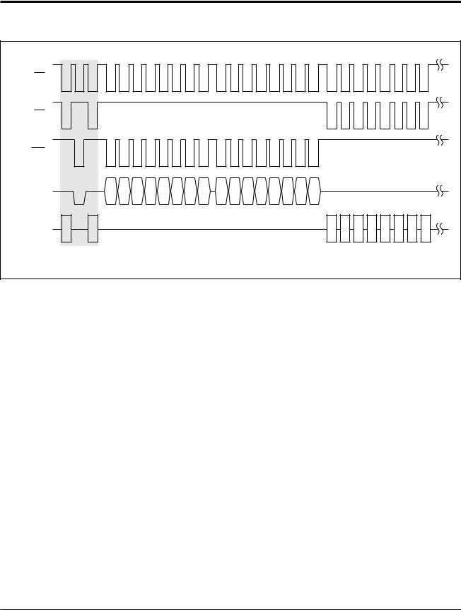
The reset sequence resets the X84041 and sets an internal write enable latch. A reset sequence can be sent at any time by performing a read/write “0”/read sequence (see Figs. 1 and 2). This sequence breaks the multiple read or write cycle sequences that are normally used when reading from or writing to the part. This sequence can be used at any time to interrupt or end a sequential read or page load. As soon as the write “0” cycle is complete, the part is reset (unless a nonvolatile write cycle is in progress). The second read cycle in this sequence, and any further read cycles, will read a HIGH on the l/O pin until a valid read sequence is issued. The reset sequence must be issued at the beginning of both read and write sequences to be sure the X84041 initiates these operations properly.
2
X84041
Figure 1. Read Sequence
CE |
|
|
|
|
|
|
|
|
|
|
|
|
|
OE |
|
|
|
|
|
|
|
|
|
|
|
|
|
WE |
|
|
|
|
|
|
|
|
|
|
|
|
|
"0" |
X |
X |
X |
X |
X |
X |
X A8 |
A7 A6 A5 |
A4 |
A3 |
A2 |
A1 |
A0 |
I/O (IN) |
|||||||||||||
I/O (OUT) |
|
|
|
|
|
|
|
|
|
|
|
|
D7 D6 D5 D4 D3 D2 D1 D0 |
RESET |
|
|
|
|
|
|
LOAD ADDRESS |
|
|
|
|
READ DATA |
|
|
|
|
|
|
|
|
|
|
|
|
|
|
2704 ILL F03 |
Write Sequence
A nonvolatile write sequence consists of sending a reset sequence, a 16-bit address (the first 7 of which are don’t cares), up to 8 bytes of data, and then a special “start nonvolatile write cycle” command sequence. The reset sequence is issued first (as described in the Reset Sequence section) to set the internal write enable latch. The address is written serially by issuing 16 separate write cycles (WE and CE LOW, OE HIGH) to the part without any read cycles between the writes. The address is sent serially, most significant bit first, on the l/O pin. Up to eight bytes of data are written by issuing either 8, 16, 24, 32, 40, 48, 56, or 64 separate write cycles. Again, no read cycles are allowed between writes. The nonvolatile write cycle is initiated by issuing a special read/write “1”/read sequence. The first read cycle ends the page load, then the write “1” followed by a read starts the nonvolatile write cycle. The X84041 recognizes 8- byte pages beginning at addresses XXXXXX000. When sending data to the part, attempts to exceed the upper address of the page will result in the address counter “wrapping-around” to the first address on the page,
where data loading can continue. For this reason, sending more than 64 consecutive data bits will result in overwriting previous data. A nonvolatile write cycle will not start if a partial or incomplete write sequence is issued. The internal write enable latch is reset when the nonvolatile write cycle is completed to prevent inadvertent writes. Note that this sequence is fully static, with no special timing restrictions. The processor is free to perform other tasks on the bus whenever the chip enable pin (CE) is HIGH.
Nonvolatile Write Status
The status of a nonvolatile write cycle can be determined at any time by simply reading the state of the l/O pin on the X84041. This pin is read when OE and CE are LOW and WE is HIGH. During a nonvolatile write cycle the l/ O pin is LOW. When the nonvolatile write cycle is complete, the l/O pin goes HIGH. A reset sequence can also be issued during a nonvolatile write cycle with the same result: I/O is LOW as long as a nonvolatile write cycle is in progress, and l/O is HIGH when the nonvolatile write cycle is done.
3

X84041
Figure 2. Write Sequence
CE |
|
|
|
|
|
|
|
|
|
|
|
|
OE |
|
|
|
|
|
|
|
|
|
|
|
|
WE |
|
|
|
|
|
|
|
|
|
|
|
|
"0" |
X |
X |
X |
X |
X |
X |
X A8 |
A7 A6 A5 |
A4 A3 A2 A1 A0 |
D7 |
D6 D5 D4 D3 D2 |
D1 D0 |
I/O (IN) |
||||||||||||
|
|
|
|
|
|
|
|
|
|
|
|
"1" |
I/O (OUT) |
|
|
|
|
|
|
|
|
|
|
|
"0" |
|
|
|
|
|
|
|
|
|
|
|
|
|
RESET |
|
|
|
|
|
|
LOAD ADDRESS |
|
LOAD DATA |
START |
||
|
|
|
|
|
|
|
|
|
|
|
|
NONVOLATILE |
|
|
|
|
|
|
|
|
|
|
|
|
WRITE |
|
|
|
|
|
|
|
|
|
|
|
|
2704 ILL F04 |
Write Protection |
|
|
|
|
|
|
|
|
SYMBOL TABLE |
|
|
|
The following circuitry has been included to prevent inadvertent nonvolatile writes:
—The internal Write Enable latch is reset upon power-up.
—A reset sequence must be issued to set the internal write enable latch before starting a write sequence.
—A special “start nonvolatile write” command sequence is required to start a nonvolatile write cycle.
—The internal Write Enable latch is reset automatically at the end of a nonvolatile write cycle.
—The internal Write Enable latch is reset and remains reset as long as the WP pin is LOW, which blocks all nonvolatile write cycles.
|
WAVEFORM INPUTS |
OUTPUTS |
|||||||||
|
|
|
|
|
|
|
|
|
|
Must be |
Will be |
|
|
|
|
|
|
|
|
|
|
||
|
|
|
|
|
|
|
|
|
|
steady |
steady |
|
|
|
|
|
|
|
|
|
|
May change |
Will change |
|
|
|
|
|
|
|
|
|
|
||
|
|
|
|
|
|
|
|
|
|
from LOW to |
from LOW to |
|
|
|
|
|
|
|
|
|
|
HIGH |
HIGH |
|
|
|
|
|
|
|
|
|
|
||
|
|
|
|
|
|
|
|
|
|
May change |
Will change |
|
|
|
|
|
|
|
|
|
|
||
|
|
|
|
|
|
|
|
|
|
from HIGH to |
from HIGH to |
|
|
|
|
|
|
|
|
|
|
LOW |
LOW |
|
|
|
|
|
|
|
|
|
|
||
|
|
|
|
|
|
|
|
|
|
Don’t Care: |
Changing: |
|
|
|
|
|
|
|
|
|
|
||
|
|
|
|
|
|
|
|
|
|
Changes |
State Not |
|
|
|
|
|
|
|
|
|
|
Allowed |
Known |
|
|
|
|
|
|
|
|
|
|
||
|
|
|
|
|
|
|
|
|
|
N/A |
Center Line |
|
|
|
|
|
|||||||
|
|
|
|
|
|
|
|
|
|
|
is High |
|
|
|
|
|
|
|
|
|
|
|
|
|
|
|
|
|
|
|
|
|
|
|
Impedance |
|
|
|
|
|
|
|
|
|
|
|
|
|
|
|
|
|
|
|
|
|
|
|
|
4
 Loading...