


XICOR X40014V8-B, X40014V8-A, X40014S8I-C, X40014S8I-B, X40014S8I-A Datasheet
...
|
New Features |
|
|
|
|
• |
Monitor Voltages: 5V to 0.9V |
Preliminary Datasheet |
• |
Independent Core Voltage Monitor |
|
|
|
|
|
|
|
X40010/X40011/X40014/X40015
Dual Voltage Monitor with Integrated CPU Supervisor
FEATURES
•Dual voltage detection and reset assertion
—Standard reset threshold settings See Selection table on page 2.
—Adjust low voltage reset threshold voltages using special programming sequence
—Reset signal valid to VCC = 1V
—Monitor three voltages or detect power fail
•Independent Core Voltage Monitor (V2MON)
•Fault detection register
•Selectable power on reset timeout (0.05s, 0.2s, 0.4s, 0.8s)
•Selectable watchdog timer interval (25ms, 200ms, 1.4s, off)
•Low power CMOS
—25µA typical standby current, watchdog on
—6µA typical standby current, watchdog off
•400kHz 2-wire interface
•2.7V to 5.5V power supply operation
•Available packages
—8-lead SOIC, TSSOP
APPLICATIONS
•Communication Equipment
—Routers, Hubs, Switches
—Disk Arrays, Network Storage
•Industrial Systems
—Process Control
—Intelligent Instrumentation
•Computer Systems
—Computers
—Network Servers
DESCRIPTION
The X40010/11/14/15 combines power-on reset control, watchdog timer, supply voltage supervision, and secondary voltage supervision, in one package. This combination lowers system cost, reduces board space requirements, and increases reliability.
Applying voltage to VCC activates the power on reset
circuit which holds RESET/RESET active for a period of time. This allows the power supply and system oscillator to stabilize before the processor can execute code.
Low VCC detection circuitry protects the user’s system from low voltage conditions, resetting the system when VCC falls below the minimum VTRIP1 point. RESET/
RESET is active until VCC returns to proper operating level and stabilizes. A second voltage monitor circuit tracks the unregulated supply to provide a power fail warning or monitors different power supply voltage. Three common low voltage combinations are available, however, Xicor’s unique circuits allows the
BLOCK DIAGRAM |
|
|
|
|
|
|
|
|
|
Watchdog Timer |
|
|
Data |
Fault Detection |
and |
WDO |
|
|
Reset Logic |
||||
|
Register |
||||
SDA |
Register |
|
|
|
|
|
|
Status |
|
|
|
|
Command |
|
|
|
|
|
Register |
|
|
||
|
Decode Test |
|
|
|
|
SCL |
& Control |
|
|
|
|
Logic |
|
|
|
|
|
|
Threshold |
|
|
|
RESET |
|
|
|
Power on, |
X40010/14 |
|
|
Reset Logic |
|
|
||
VCC |
|
+ |
|
Low Voltage |
RESET |
|
|
Reset |
X40011/15 |
||
(V1MON) |
|
|
|
Generation |
|
User Programmable |
- |
|
|
||
|
|
|
|
||
|
VTRIP1 |
|
V2MON |
|
|
V2MON |
|
+ |
VCC |
|
V2FAIL |
|
|
|
|||
|
|
|
User Programmable |
|
|
|
- |
|
|
|
|
|
|
|
|
|
|
|
|
|
|
|
|
|
|
|
|
|
|
||
|
|
|
VTRIP2 |
|
|
|
*X40010/11 = V2MON* |
|
|
|
|
|
|
|
|
|
|
|
|
|
|
|
|
|
|
|
|
|
|
||
|
|
|
|
|
|
|
|
||||||||
|
|
|
|
|
|
|
X40014/15 = VCC |
|
|
|
|
|
|
|
|
|
|
|
|
|
|
|
|
|
|
|
|
|
|
|
|
REV 1.3.4 7/12/02 |
www.xicor.com |
Characteristics subject to change without notice. 1 of 25 |
|||||||||||||

X40010/X40011/X40014/X40015 – Preliminary
threshold for either voltage monitor to be reprogrammed to meet special needs or to fine-tune the threshold for applications requiring higher precision.
The Watchdog Timer provides an independent protection mechanism for microcontrollers. When the microcontroller fails to restart a timer within a selectable time out interval, the device activates the WDO signal. The user selects the interval from three preset values. Once selected, the interval does not change, even after cycling the power.
The device features a 2-wire interface and software protocol allowing operation on an I2C® bus.
Dual Voltage Monitors
Device |
Expected System Voltages |
Vtrip1(V) |
Vtrip2(V) |
POR (system) |
|
|
|
|
|
X40010/11 |
|
2.0–4.75* |
1.70–4.75 |
RESET = X40010 |
-A |
5V; 3V or 3.3V |
4.55–4.65* |
2.85–2.95 |
|
-B |
5V; 3V |
4.35–4.45* |
2.55–2.65 |
RESET = X40011 |
-C |
3V; 3.3V; 1.8V |
2.85–2.95* |
1.65–1.75 |
|
|
|
|
|
|
X40014/15 |
|
2.0–4.75* |
0.90–3.50* |
RESET = X40014 |
-A |
3V; 3.3V; 1.5V |
2.85–2.95* |
1.25–1.35* |
|
-B |
3V; 1.5V |
2.55–2.65* |
1.25–1.35* |
RESET = X40015 |
-C |
3V or 3.3V; 1.1 or 1.2V |
2.85–2.95* |
0.95–1.05* |
|
|
|
|
|
|
*Voltage monitor requires VCC to operation. Others are independent of VCC.
PIN CONFIGURATION
|
|
|
|
X40010/14, X40011/15 |
|
|
|
|
X40010/14, X40011/15 |
|
|
|
||||||||
|
|
|
|
|
|
8-Pin SOIC |
|
|
|
|
|
8-Pin TSSOP |
|
|
|
|||||
|
|
|
|
|
1 |
8 |
|
|
VCC |
|
|
|
|
1 |
8 |
|
|
SCL |
|
|
|
|
|
V2FAIL |
|
|
|
|
WDO |
|
|
|
|
||||||||
|
|
|
|
|||||||||||||||||
|
|
V2MON |
|
2 |
7 |
|
|
WDO |
|
|
VCC |
|
2 |
7 |
|
|
SDA |
|
||
|
|
|
|
|
|
|
|
|||||||||||||
|
|
|
|
|
3 |
6 |
|
|
SCL |
|
V2FAIL |
|
3 |
6 |
|
|
VSS |
|
|
|
|
RESET/RESET |
|
|
|
|
|||||||||||||||
|
|
|
|
|
|
|
||||||||||||||
|
|
|
VSS |
|
4 |
5 |
|
|
SDA |
V2MON |
|
4 |
5 |
|
|
RESET/RESET |
|
|||
|
|
|
|
|
|
|
|
|||||||||||||
|
|
|
|
|
|
|
|
|||||||||||||
|
|
|
|
|
|
|
|
|
|
|
|
|
|
|
|
|
|
|
|
|
PIN DESCRIPTION
|
Pin |
|
|
|
|
|
|
|
|
|
|
|
|
|
|
|
Name |
|
|
Function |
|
|
|
||||
SOIC |
TSSOP |
|
|
|
|
|
|
|
|||||
|
|
|
|
|
|
|
|
|
|
||||
1 |
|
3 |
|
|
|
|
|
|
V2 Voltage Fail Output. This open drain output goes LOW when V2MON is less than VTRIP2 and |
||||
V2FAIL |
|||||||||||||
|
|
|
|
|
|
|
|
|
goes HIGH when V2MON exceeds VTRIP2. There is no power up reset delay circuitry on this pin. |
||||
2 |
|
4 |
|
V2MON |
|
V2 Voltage Monitor Input. When the V2MON input is less than the VTRIP2 voltage, |
|
goes |
|||||
V2FAIL |
|||||||||||||
|
|
|
|
|
|
|
|
|
LOW. This input can monitor an unregulated power supply with an external resistor divider or can |
||||
|
|
|
|
|
|
|
|
|
monitor a second power supply with no external components. Connect V2MON to VSS or VCC |
||||
|
|
|
|
|
|
|
|
|
when not used.The V2MON comparator is supplied by V2MON (X40010/11) or by VCC Input |
||||
|
|
|
|
|
|
|
|
|
(X40014/15). |
|
|
|
|
3 |
|
5 |
|
|
|
|
|
|
Output. (X40011/15) This is an active LOW, open drain output which goes active when- |
||||
RESET/ |
RESET |
||||||||||||
|
|
|
|
|
RESET |
|
ever VCC falls below VTRIP1. It will remain active until VCC rises above VTRIP1 and for the tPURST |
||||||
|
|
|
|
|
|
|
|
|
thereafter. |
|
|
|
|
|
|
|
|
|
|
|
|
|
RESET Output. (X40010/14) This is an active HIGH CMOS output which goes active whenever |
||||
|
|
|
|
|
|
|
|
|
VCC falls below VTRIP1. It will remain active until VCC rises above VTRIP1 and for the tPURST there- |
||||
|
|
|
|
|
|
|
|
|
after. |
|
|
|
|
4 |
|
6 |
|
|
VSS |
|
Ground |
|
|
|
|||
|
|
|
|
|
|
|
|
|
|
|
|
|
|
REV 1.3.4 7/12/02 |
|
|
|
|
|
|
www.xicor.com |
Characteristics subject to change without notice. 2 of 25 |
|||||
X40010/X40011/X40014/X40015 – Preliminary
PIN DESCRIPTION (Continued)
|
Pin |
|
|
|
|
|
|
|
|
|
|
Name |
|
|
|
|
Function |
||||
SOIC |
TSSOP |
|
|
|
|
|||||
|
|
|
|
|
|
|
||||
5 |
|
7 |
|
SDA |
|
Serial Data. SDA is a bidirectional pin used to transfer data into and out of the device. It has an |
||||
|
|
|
|
|
|
|
open drain output and may be wire ORed with other open drain or open collector outputs. This pin |
|||
|
|
|
|
|
|
|
requires a pull up resistor and the input buffer is always active (not gated). |
|||
|
|
|
|
|
|
|
Watchdog Input. A HIGH to LOW transition on the SDA (while SCL is toggled from HIGH to |
|||
|
|
|
|
|
|
|
LOW and followed by a stop condition) restarts the Watchdog timer. The absence of this tran- |
|||
|
|
|
|
|
|
|
sition within the watchdog time out period results in WDO going active. |
|||
|
|
|
|
|
|
|
||||
6 |
|
8 |
|
SCL |
|
Serial Clock. The Serial Clock controls the serial bus timing for data input and output. |
||||
|
|
|
|
|
|
|
|
|
|
|
7 |
|
1 |
|
|
|
|
|
Output. |
|
is an active LOW, open drain output which goes active whenever the |
WDO |
WDO |
WDO |
||||||||
|
|
|
|
|
|
|
watchdog timer goes active. |
|||
|
|
|
|
|
|
|
||||
8 |
|
2 |
|
VCC |
|
Supply Voltage |
||||
PRINCIPLES OF OPERATION
Power On Reset
Application of power to the X40010/11/14/15 activates a Power On Reset Circuit that pulls the RESET/RESET pins active.This signal provides several benefits.
–It prevents the system microprocessor from starting to operate with insufficient voltage.
–It prevents the processor from operating prior to stabilization of the oscillator.
–It allows time for an FPGA to download its configuration prior to initialization of the circuit.
–It prevents communication to the EEPROM, greatly reducing the likelihood of data corruption on power up.
When VCC exceeds the device VTRIP1 threshold value for tPURST (selectable) the circuit releases the RESET
(X40011) and RESET (X40010) pin allowing the system to begin operation.
Low Voltage VCC (V1 Monitoring)
During operation, the X40010/11/14/15 monitors the VCC
level and asserts RESET/RESET if supply voltage falls below a preset minimum VTRIP1. The RESET/RESET signal prevents the microprocessor from operating in a power fail or brownout condition. The V1FAIL signal remains active until the voltage drops below 1V. It also remains active until VCC returns and exceeds VTRIP1 for
tPURST.
Low Voltage V2 Monitoring
The X40010/11/14/15 also monitors a second voltage
level and asserts V2FAIL if the voltage falls below a preset minimum VTRIP2. The V2FAIL signal is either ORed with RESET to prevent the microprocessor from operating in a power fail or brownout condition or used to interrupt the microprocessor with notification of an
impending power failure. For the X40010/11 the V2FAIL signal remains active until the VCC drops below 1V (VCC falling). It also remains active until V2MON returns and
exceeds VTRIP2 by 0.2V. This voltage sense circuitry monitors the power supply connected to the V2MON pin.
If VCC = 0, V2MON can still be monitored.
For the X40014/15 devices, the V2FAIL signal remains actice until VCC drops below 1Vx and remains active until
V2MON returns and exceeds VTRIP2. This sense circuitry is powered by VCC. If VCC = 0, V2MON cannot be monitored.
Figure 1. Two Uses of Multiple Voltage Monitoring
|
|
X40011-A |
VCC V2MON |
|
|
|
|
||
6–10V |
5V |
VCC |
System |
|
Reg |
||||
|
RESET |
Reset |
||
1M |
|
|||
|
V2MON |
|
||
|
|
|
||
|
|
(2.9V) |
|
|
1M |
|
V2FAIL |
|
|
|
|
|
Resistors selected so 3V appears on V2MON when unregulated
|
|
|
|
supply reaches 6V. |
|
|
|||
|
|
|
|
|
X40014-C |
VCC |
|||
|
|
|
|
|
|
|
|||
Unreg. |
|
3.3V |
|
VCC |
|
|
|||
Supply |
|
|
Reg |
|
|
System |
|||
|
|
|
|
|
|
|
|
|
|
|
|
|
|
|
|
RESET |
|||
|
|
|
1.2V |
|
V2MON |
|
Reset |
||
|
|
|
|
|
|
||||
|
|
|
Reg |
|
|
|
|||
|
|
|
|
|
|
|
|
|
|
|
|
|
|
|
|
|
|
|
|
|
|
|
|
|
|
|
|
|
|
|
|
|
|
|
|
V2FAIL |
|
|
|
|
|
|
|
|
|
|
|
|
|
|
|
|
|
|
|
|
|
|
|
Notice: No external components required to monitor two voltages.
REV 1.3.4 7/12/02 |
www.xicor.com |
Characteristics subject to change without notice. 3 of 25 |
X40010/X40011/X40014/X40015 – Preliminary
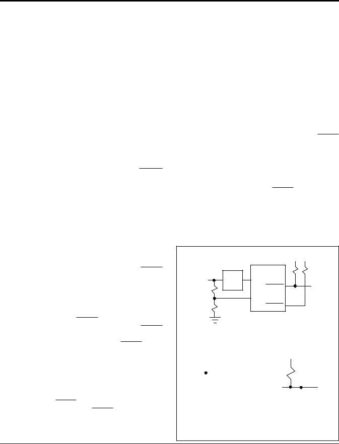
Figure 2. VTRIPX Set/Reset Conditions
|
VTRIPX |
(X = 1, 2) |
VCC/V2MON |
|
||
|
|
|
|
|
VP |
|
WDO |
|
|
|
|
|
|
SCL |
0 |
7 |
0 |
7 |
0 |
7 |
|
||||||
|
|
|
|
|
|
|
SDA |
|
|
|
|
|
|
|
A0h |
|
|
|
00h |
tWC |
WATCHDOG TIMER
The Watchdog Timer circuit monitors the microprocessor activity by monitoring the SDA and SCL pins. The microprocessor must toggle the SDA pin HIGH to LOW periodically, while SCL also toggles from HIGH to LOW (this is a start bit) followed by a stop condition prior to the expiration of the watchdog time out period to prevent a WDO signal going active. The state of two nonvolatile control bits in the Status Register determines the watchdog timer period. The microprocessor can change these watchdog bits by writing to the X40010/ 11/14/15 control register (also refer to page 19).
Figure 3. Watchdog Restart
.6µs
1.3µs
SCL
SDA
Timer Start
V1 AND V2 THRESHOLD PROGRAM PROCEDURE (OPTIONAL)
The X40010/11/14/15is shipped with standard V1 and
V2 threshold (VTRIP1, VTRIP2) voltages. These values will not change over normal operating and storage con-
ditions. However, in applications where the standard thresholds are not exactly right, or if higher precision is needed in the threshold value, the X40010/11/14/15trip
points may be adjusted. The procedure is described below, and uses the application of a high voltage control signal.
Setting a VTRIPx Voltage (x=1, 2)
There are two procedures used to set the threshold voltages (VTRIPx), depending if the threshold voltage to be stored is higher or lower than the present value. For
example, if the present VTRIPx is 2.9 V and the new VTRIPx is 3.2 V, the new voltage can be stored directly into the VTRIPx cell. If however, the new setting is to be lower than the present setting, then it is necessary to
“reset” the V voltage before setting the new value.
TRIPx
Setting a Higher VTRIPx Voltage (x=1, 2)
To set a VTRIPx threshold to a new voltage which is higher than the present threshold, the user must apply
the desired VTRIPx threshold voltage to the corresponding input pin Vcc(V1MON), or V2MON. The
Vcc(V1MON) and V2MON must be tied together during this sequence. Then, a programming voltage (Vp) must be applied to the WDO pin before a START condition is set up on SDA. Next, issue on the SDA pin the Slave Address A0h, followed by the Byte Address 01h for
VTRIP1 and 09h for VTRIP2, and a 00h Data Byte in order to program VTRIPx. The STOP bit following a valid write operation initiates the programming
sequence. Pin WDO must then be brought LOW to complete the operation.
Note: This operation does not corrupt the memory array.
REV 1.3.4 7/12/02 |
www.xicor.com |
Characteristics subject to change without notice. 4 of 25 |
X40010/X40011/X40014/X40015 – Preliminary
Setting a Lower VTRIPx Voltage (x=1, 2)
In order to set VTRIPx to a lower voltage than the present value, then VTRIPx must first be “reset” according to the procedure described below. Once VTRIPx
has been “reset”, then V can be set to the desired
TRIPx
voltage using the procedure described in “Setting a Higher VTRIPx Voltage”.
Resetting the VTRIPx Voltage
To reset a VTRIPx voltage, apply the programming voltage (Vp) to the WDO pin before a START condition is
set up on SDA. Next, issue on the SDA pin the Slave Address A0h followed by the Byte Address 03h for
VTRIP1 and 0Bh for VTRIP2, followed by 00h for the Data Byte in order to reset VTRIPx. The STOP bit following a valid write operation initiates the programming
sequence. Pin WDO must then be brought LOW to complete the operation.
After being reset, the value of VTRIPx becomes a nominal value of 1.7V or lesser.
Note: This operation does not corrupt the memory array.
CONTROL REGISTER
The Control Register provides the user a mechanism for changing the Block Lock and Watchdog Timer settings. The Block Lock and Watchdog Timer bits are nonvolatile and do not change when power is removed.
The Control Register is accessed with a special preamble in the slave byte (1011) and is located at address 1FFh. It can only be modified by performing a byte write operation directly to the address of the register and only one data byte is allowed for each register write operation. Prior to writing to the Control Register, the WEL and RWEL bits must be set using a two step process, with the whole sequence requiring 3 steps. See "Writing to the Control Registers" on page 7.
The user must issue a stop, after sending this byte to the register, to initiate the nonvolatile cycle that stores WD1, WD0, PUP1, PUP0, BP1, and BP0. The X40010/ 11/14/15 will not acknowledge any data bytes written after the first byte is entered.
The state of the Control Register can be read at any time by performing a random read at address 01Fh, using the special preamble. Only one byte is read by each register read operation. The master should supply a stop condition to be consistent with the bus protocol, but a stop is not required to end this operation.
7 |
6 |
5 |
4 |
3 |
2 |
1 |
0 |
|
|
|
|
|
|
|
|
PUP1 |
WD1 |
WD0 |
BP |
0 |
RWEL |
WEL |
PUP0 |
|
|
|
|
|
|
|
|
RWEL: Register Write Enable Latch (Volatile)
The RWEL bit must be set to “1” prior to a write to the Control Register.
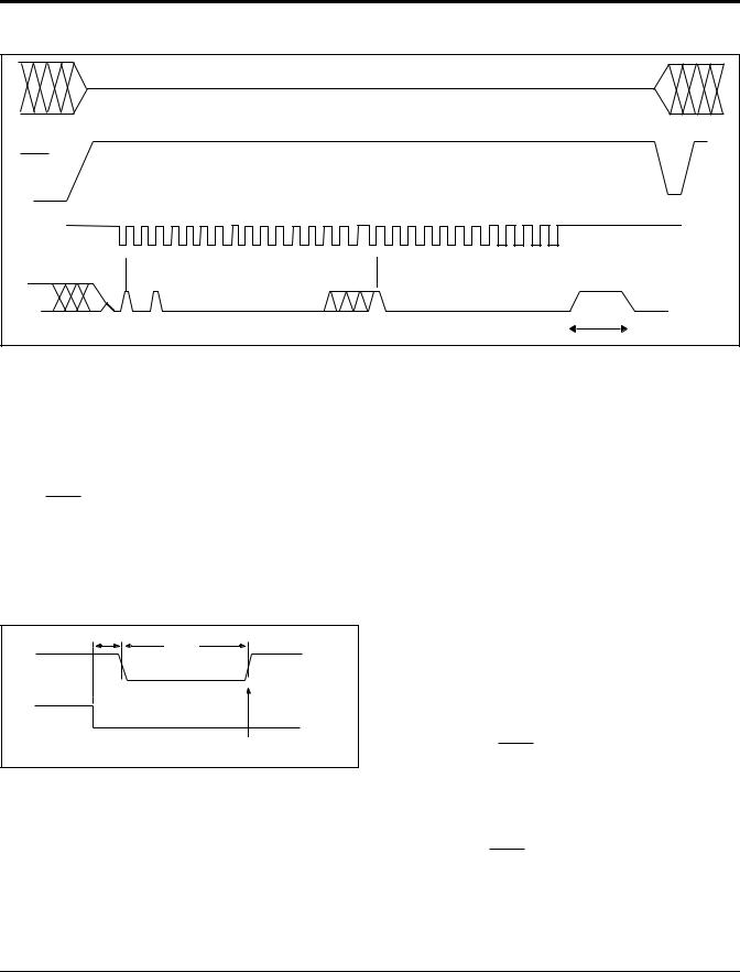
Figure 4. Sample VTRIP Reset Circuit
|
|
|
|
|
VP |
|
|
V2FAIL |
|
|
Adjust |
|
|
|
8 |
µC |
|
|
|
1 |
|
|
|
|
|
RESET |
SOIC |
7 |
|
|
|
3 |
Run |
||
VTRIP1 |
|
2 |
X4001x |
6 |
|
|
|
||||
Adj. |
|
4 |
|
5 |
SCL |
|
VTRIP2 |
4.7K |
|
|
SDA |
|
Adj. |
|
|
||
|
|
|
|
|
REV 1.3.4 7/12/02 |
www.xicor.com |
Characteristics subject to change without notice. 5 of 25 |

X40010/X40011/X40014/X40015 – Preliminary
Figure 5. VTRIPX Set/Reset Sequence (X = 1, 2)
|
VTRIPX Programming |
Vx = VCC, VxMON |
|
|
|
Note: X = 1, 2 |
|
|
|
Let: MDE = Maximum Desired Error |
|
No |
Desired |
|
|
|
VTRIPX |
MDE |
+ |
|
Present Value |
|
|
|
|
Acceptable |
|
|
|
|
|
|
YES |
Desired Value |
|
|
|
Error Range |
|
|
|
|
|
|
Execute |
MDE– |
|
|
VTRIPX Reset Sequence |
|
|
|
|
Error = Actual - Desired |
|
|
Execute |
|
|
|
Set Higher VTRIPX Sequence |
|
|
New VX applied = |
Execute |
New VX applied = |
|
Old VX applied + | Error | |
Set Higher VX Sequence |
Old VX applied - | Error | |
|
|
Apply VCC and Voltage |
Execute Reset VTRIPX |
|
|
> Desired VTRIPX to VX |
Sequence |
|
NO |
|
|
|
|
Decrease VX |
|
|
|
Output Switches? |
|
|
|
YES |
|
|
Error < MDE– |
Actual VTRIPX - |
Error > MDE+ |
|
|
Desired VTRIPX |
|
|
|
| Error | < | MDE | |
|
|
|
DONE |
|
|
WEL: Write Enable Latch (Volatile)
The WEL bit controls the access to the memory and to the Register during a write operation. This bit is a volatile latch that powers up in the LOW (disabled) state. While the WEL bit is LOW, writes to any address, including any control registers will be ignored (no acknowledge will be issued after the Data Byte). The WEL bit is set by writing a “1” to the WEL bit and zeros to the other bits of the control register.
Once set, WEL remains set until either it is reset to 0 (by writing a “0” to the WEL bit and zeros to the other bits of the control register) or until the part powers up again. Writes to the WEL bit do not cause a high voltage write cycle, so the device is ready for the next operation immediately after the stop condition.
REV 1.3.4 7/12/02 |
www.xicor.com |
Characteristics subject to change without notice. 6 of 25 |

X40010/X40011/X40014/X40015 – Preliminary
PUP1, PUP0: Power Up Bits (Nonvolatile)
The Power Up bits, PUP1 and PUP0, determine the
tPURST time delay. The nominal power up times are shown in the following table.
PUP1 |
PUP0 |
Power on Reset Delay (tPURST) |
0 |
0 |
50ms |
|
|
|
0 |
1 |
200ms (factory setting) |
|
|
|
1 |
0 |
400ms |
|
|
|
1 |
1 |
800ms |
|
|
|
WD1, WD0: Watchdog Timer Bits (Nonvolatile)
The bits WD1 and WD0 control the period of the Watchdog Timer. The options are shown below.
WD1 |
WD0 |
Watchdog Time Out Period |
|
|
|
0 |
0 |
1.4 seconds |
|
|
|
0 |
1 |
200 milliseconds |
|
|
|
1 |
0 |
25 milliseconds |
|
|
|
1 |
1 |
disabled (factory setting) |
|
|
|
Writing to the Control Registers
Changing any of the nonvolatile bits of the control and trickle registers requires the following steps:
–Write a 02H to the Control Register to set the Write Enable Latch (WEL). This is a volatile operation, so there is no delay after the write. (Operation preceded by a start and ended with a stop).
–Write a 06H to the Control Register to set the Register Write Enable Latch (RWEL) and the WEL bit. This is also a volatile cycle. The zeros in the data byte are required. (Operation proceeded by a start and ended with a stop).
–Write a one byte value to the Control Register that has all the control bits set to the desired state. The Control register can be represented as qxys 001r in binary, where xy are the WD bits, s isthe BP bit and qr are the power up bits. This operation proceeded by a start and ended with a stop bit. Since this is a
nonvolatile write cycle it will take up to 10ms to complete. The RWEL bit is reset by this cycle and the sequence must be repeated to change the nonvolatile bits again. If bit 2 is set to ‘1’ in this third step (qxys 011r) then the RWEL bit is set, but the WD1, WD0, PUP1, PUP0, and BP bits remain unchanged. Writing a second byte to the control register is not allowed. Doing so aborts the write operation and returns a NACK.
–A read operation occurring between any of the previous operations will not interrupt the register write operation.
–The RWEL bit cannot be reset without writing to the nonvolatile control bits in the control register, power cycling the device or attempting a write to a write protected block.
To illustrate, a sequence of writes to the device consisting of [02H, 06H, 02H] will reset all of the nonvolatile bits in the Control Register to 0. A sequence of [02H, 06H, 06H] will leave the nonvolatile bits unchanged and the RWEL bit remains set.
FAULT DETECTION REGISTER
The Fault Detection Register (FDR) provides the user the status of what causes the system reset active. The Manual Reset Fail, Watchdog Timer Fail and three Low Voltage Fail bits are volatile.
7 |
6 |
5 |
4 |
3 |
2 |
1 |
0 |
|
|
|
|
|
|
|
|
LV1F |
LV2F |
0 |
WDF |
0 |
0 |
0 |
0 |
|
|
|
|
|
|
|
|
The FDR is accessed with a special preamble in the slave byte (1011) and is located at address 0FFh. It can only be modified by performing a byte write operation directly to the address of the register and only one data byte is allowed for each register write operation.
There is no need to set the WEL or RWEL in the control register to access this fault detection register.
REV 1.3.4 7/12/02 |
www.xicor.com |
Characteristics subject to change without notice. 7 of 25 |
X40010/X40011/X40014/X40015 – Preliminary
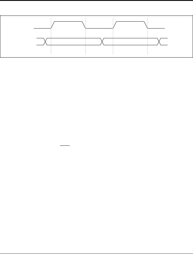
Figure 6. Valid Data Changes on the SDA Bus
SCL
SDA
Data Stable |
Data Change |
Data Stable |
At power-up, the Fault Detection Register is defaulted to all “0”. The system needs to initialize this register to all “1” before the actual monitoring take place. In the event of any one of the monitored sources failed. The corresponding bits in the register will change from a “1” to a “0” to indicate the failure. At this moment, the system should perform a read to the register and noted the cause of the reset. After reading the register the system should reset the register back to all “1” again. The state of the Fault Detection Register can be read at any time by performing a random read at address 0FFh, using the special preamble.
The FDR can be read by performing a random read at OFFh address of the register at any time. Only one byte of data is read by the register read operation.
WDF, Watchdog Timer Fail Bit (Volatile)
The WDF bit will set to “0” when the WDOgoes active.
LV1F, Low VCC Reset Fail Bit (Volatile)
The LV1F bit will be set to “0” when V (V1MON) falls
CC
below VTRIP1.
LV2F, Low V2MON Reset Fail Bit (Volatile)
The LV2F bit will be set to “0” when V2MON falls below VTRIP2.
SERIAL INTERFACE
Interface Conventions
The device supports a bidirectional bus oriented protocol. The protocol defines any device that sends data onto the bus as a transmitter, and the receiving device as the receiver. The device controlling the transfer is called the master and the device being controlled is called the slave. The master always initiates data transfers, and provides the clock for both transmit and receive operations. Therefore, the devices in this family operate as slaves in all applications.
Serial Clock and Data
Data states on the SDA line can change only during SCL LOW. SDA state changes during SCL HIGH are reserved for indicating start and stop conditions. See Figure 6.
Serial Start Condition
All commands are preceded by the start condition, which is a HIGH to LOW transition of SDA when SCL is HIGH. The device continuously monitors the SDA and SCL lines for the start condition and will not respond to any command until this condition has been met. See Figure 6.
Serial Stop Condition
All communications must be terminated by a stop condition, which is a LOW to HIGH transition of SDA when SCL is HIGH. The stop condition is also used to place the device into the Standby power mode after a read sequence. A stop condition can only be issued after the transmitting device has released the bus. See Figure 6.
REV 1.3.4 7/12/02 |
www.xicor.com |
Characteristics subject to change without notice. 8 of 25 |
 Loading...