


XICOR X28C010TMB-12, X28C010TM-25, X28C010TM-20, X28C010TM-15, X28C010TM-12 Datasheet
...
X28C010
1M |
X28C010 |
128K x 8 Bit |
5 Volt, Byte Alterable E2PROM
FEATURES
•Access Time: 120ns
•Simple Byte and Page Write —Single 5V Supply
—No External High Voltages or V PP Control Circuits —Self-Timed
—No Erase Before Write
—No Complex Programming Algorithms —No Overerase Problem
•Low Power CMOS:
—Active: 50mA —Standby: 500 μA
•Software Data Protection
—Protects Data Against System Level Inadvertant Writes
•High Speed Page Write Capability
•Highly Reliable Direct Write™ Cell —Endurance: 100,000 Write Cycles —Data Retention: 100 Years
•Early End of Write Detection
— DATA Polling
—Toggle Bit Polling
DESCRIPTION
The Xicor X28C010 is a 128K x 8 E2PROM, fabricated with Xicor's proprietary, high performance, floating gate CMOS technology. Like all Xicor programmable nonvolatile memories the X28C010 is a 5V only device. The X28C010 features the JEDEC approved pinout for bytewide memories, compatible with industry standard EPROMs.
The X28C010 supports a 256-byte page write operation, effectively providing a 19μs/byte write cycle and enabling the entire memory to be typically written in less than 2.5 seconds. The X28C010 also features DATA Polling and Toggle Bit Polling, system software support schemes used to indicate the early completion of a write cycle. In addition, the X28C010 supports Software Data Protection option.
Xicor E2PROMs are designed and tested for applications requiring extended endurance. Data retention is specified to be greater than 100 years.
PIN CONFIGURATIONS
|
|
|
CERDIP |
|
|
|
|
|
|
|
|
|
|
|
|
|
|
|
|
|
|
|
|
||
|
|
FLAT PACK |
|
|
|
|
|
|
|
|
|
|
|
|
|
|
|
|
|
|
|
|
|||
|
|
|
SOIC (R) |
|
|
|
|
|
|
|
|
|
PGA |
|
|
|
|
|
|
|
|
|
|
||
|
|
|
|
|
|
|
|
|
|
|
|
|
|
|
|
|
|
|
|
|
|
|
|
||
NC |
|
1 |
32 |
|
VCC |
|
|
I/O0 |
I/O2 |
I/O3 |
I/O5 |
I/O6 |
|
|
|
|
|
||||||||
|
|
|
|
15 |
|
17 |
19 |
21 |
|
22 |
|
|
|
|
|
|
|||||||||
|
|
|
|
|
|
|
|
|
|
||||||||||||||||
A16 |
|
2 |
31 |
|
|
WE |
|
|
|
|
|
|
|
|
|
|
|
||||||||
|
|
|
|
A1 |
A0 |
I/O1 |
VSS |
I/O4 |
I/O7 |
CE |
|||||||||||||||
|
|||||||||||||||||||||||||
A15 |
|
3 |
30 |
|
NC |
13 |
|
14 |
|
16 |
18 |
20 |
|
23 |
|
24 |
|
|
|
||||||
|
|
|
|
|
|
|
|
|
|
|
|
|
|
|
|
|
|
||||||||
A12 |
|
4 |
29 |
|
A14 |
A2 |
A3 |
|
|
|
|
|
A10 |
|
OE |
|
|||||||||
|
|
|
|
|
|
|
|||||||||||||||||||
|
|
12 |
|
11 |
|
|
|
|
|
|
25 |
|
26 |
|
|
|
|||||||||
A7 |
|
5 |
28 |
|
A13 |
A |
4 |
A |
5 |
X28C010 |
|
|
|
A |
11 |
A |
9 |
|
|
||||||
|
|
|
|
|
|
||||||||||||||||||||
A6 |
|
6 |
27 |
|
A8 |
10 |
|
9 |
|
(BOTTOM VIEW) |
27 |
|
28 |
|
|
|
|||||||||
|
|
|
|
|
|
|
|
|
|
|
|
|
|||||||||||||
A5 |
|
7 |
26 |
|
A9 |
A6 |
A7 |
|
|
|
|
|
A8 |
A13 |
|||||||||||
|
|
|
|
|
|
||||||||||||||||||||
A4 |
|
8 |
25 |
|
A11 |
8 |
|
7 |
|
|
|
|
|
|
29 |
|
30 |
|
|
|
|||||
|
|
|
|
|
|
|
|
|
|
|
|
|
|
|
|
|
|
||||||||
|
|
|
|
|
|
|
|
|
|
|
|
|
|
|
|
|
|||||||||
|
|
|
X28C010 |
|
|
|
|
A12 |
A15 |
NC |
VCC |
NC |
NC |
A14 |
|||||||||||
A3 |
|
9 |
24 |
|
OE |
6 |
|
5 |
|
2 |
36 |
34 |
|
32 |
|
31 |
|
|
|
||||||
|
|
|
|
|
|
|
|||||||||||||||||||
A2 |
|
10 |
23 |
|
A10 |
|
|
A16 |
NC |
NC |
|
|
|
NC |
|
|
|
|
|
||||||
|
|
|
|
|
|
|
|
|
|
|
|||||||||||||||
|
|
|
|
|
|
|
|
WE |
|
|
|
|
|
||||||||||||
A1 |
|
11 |
22 |
|
|
|
|
|
|
|
|
|
|
|
|||||||||||
|
|
CE |
|
|
|
|
|
|
|
||||||||||||||||
|
|
|
|
4 |
|
3 |
1 |
35 |
|
33 |
|
|
|
|
|
|
|||||||||
|
|
|
|
|
|
|
|
|
|
|
|||||||||||||||
A0 |
|
12 |
21 |
|
I/O7 |
|
|
|
|
|
|
|
|
|
3858 FHD F20 |
||||||||||
I/O0 |
|
13 |
20 |
|
I/O6 |
|
|
|
|
|
|
|
|
|
|||||||||||
|
|
|
|
|
|
|
|
|
|
|
|
|
|
|
|
|
|
||||||||
I/O1 |
|
14 |
19 |
|
I/O5 |
|
|
|
|
|
|
|
|
|
|
|
|
|
|
|
|
||||
|
|
|
|
|
|
|
|
|
|
|
|
|
|
|
|
|
|
||||||||
I/O2 |
|
15 |
18 |
|
I/O4 |
|
|
|
|
|
|
|
|
|
|
|
|
|
|
|
|
||||
|
|
|
|
|
|
|
|
|
|
|
|
|
|
|
|
|
|||||||||
VSS |
|
16 |
17 |
|
I/O3 |
|
|
|
|
|
|
|
|
|
|
|
|
|
|
|
|
||||
|
|
|
|
|
|
|
|
|
|
|
|
|
|
|
|
|
|||||||||
3858 FHD F02.1
© Xicor, Inc. 1991, 1995, 1996 Patents Pending |
1 |
|
3858-3.1 4/3/97 T1/C0/D0 SH |
||
|
|
|
|
PLCC |
|
|
|
|
EXTENDED LCC |
|
||||||||
|
|
|
|
|
|
|
|
|
|
|
CC |
|
|
|
|||
|
|
|
LCC |
|
|
|
|
12 |
15 |
16 |
NC |
WE |
NC |
|
|||
|
12 |
15 |
16 |
|
CC |
|
|
|
|
A |
A |
A |
V |
|
|||
|
NC |
WE |
NC |
|
|
|
|
|
|
|
|
30 |
|
||||
|
A |
A |
A |
V |
|
|
4 |
3 |
2 |
|
32 31 |
|
|||||
|
|
|
|
|
|
|
30 |
|
|
|
|
|
|||||
|
|
|
|
|
|
|
|
|
|
|
|
1 |
|
|
|
|
|
A7 |
5 4 3 |
2 |
1 |
32 31 29 |
A14 |
A7 |
5 |
|
|
|
|
|
29 |
A14 |
|||
A6 |
6 |
|
|
|
|
28 |
A13 |
A6 |
6 |
|
|
|
|
|
28 |
A13 |
|
|
|
|
|
|
|
|
|
|
|
||||||||
A5 |
7 |
|
|
|
|
|
27 |
A8 |
A5 |
7 |
|
|
|
|
|
27 |
A8 |
A4 |
8 |
|
X28C010 |
|
26 |
A9 |
A4 |
8 |
|
X28C010 |
|
26 |
A9 |
||||
A3 |
9 |
|
|
25 |
A11 |
A3 |
9 |
|
|
25 |
A11 |
||||||
(TOP VIEW) |
(TOP VIEW) |
||||||||||||||||
A2 |
10 |
|
|
|
|
|
24 |
OE |
A2 |
10 |
|
|
|
|
|
24 |
OE |
A1 |
11 |
|
|
|
|
|
23 |
A10 |
A1 |
11 |
|
|
|
|
|
23 |
A10 |
A0 |
12 |
|
|
|
|
|
22 |
CE |
A0 |
12 |
|
|
|
|
|
22 |
CE |
I/O0 |
13 |
15 16 17 18 19 20 21 |
I/O7 |
I/O0 |
13 |
|
|
|
|
|
21 |
I/O7 |
|||||
|
14 |
|
|
|
|
|
|
|
|
|
|
|
|
|
|
|
|
|
1 |
2 |
SS |
3 |
4 |
5 6 |
|
|
14 15 16 17 18 19 20 |
|
|||||||
|
|
|
|
|
|
|
|
|
|
|
|||||||
|
I/O |
I/O |
V |
I/O |
I/O |
I/O |
I/O |
|
|
1 |
2 |
SS |
3 |
4 |
5 6 |
|
|
|
|
|
|
|
|
|
|
|
|
|
|||||||
|
|
|
|
|
|
|
|
|
|
I/O |
I/O |
V |
I/O |
I/O |
I/O |
I/O |
|
|
|
|
|
|
|
|
|
|
TSOP |
|
|
|
|
|
3858 FHD F03.1 |
||
|
|
|
|
|
|
|
|
|
|
|
|
|
|
|
|
|
|
A11 |
|
1 |
|
|
|
|
|
|
|
|
|
|
|
|
40 |
OE |
|
A9 |
|
2 |
|
|
|
|
|
|
|
|
|
|
|
|
39 |
A10 |
|
A8 |
|
3 |
|
|
|
|
|
|
|
|
|
|
|
|
38 |
CE |
|
A13 |
|
4 |
|
|
|
|
|
|
|
|
|
|
|
|
37 |
I/O7 |
|
A14 |
|
5 |
|
|
|
|
|
|
|
|
|
|
|
|
36 |
I/O6 |
|
NC |
|
6 |
|
|
|
|
|
|
|
|
|
|
|
|
35 |
I/O5 |
|
NC |
|
7 |
|
|
|
|
|
|
|
|
|
|
|
|
34 |
I/O4 |
|
NC |
|
8 |
|
|
|
|
|
|
|
|
|
|
|
|
33 |
I/O3 |
|
WE |
|
9 |
|
|
|
|
|
|
|
|
|
|
|
|
32 |
NC |
|
VCC |
|
10 |
|
|
|
|
|
X28C010 |
|
|
|
|
|
31 |
NC |
||
NC |
|
11 |
|
|
|
|
|
|
|
|
|
|
|
|
30 |
VSS |
|
NC |
|
12 |
|
|
|
|
|
|
|
|
|
|
|
|
29 |
NC |
|
NC |
|
13 |
|
|
|
|
|
|
|
|
|
|
|
|
28 |
NC |
|
A16 |
|
14 |
|
|
|
|
|
|
|
|
|
|
|
|
27 |
I/O2 |
|
A15 |
|
15 |
|
|
|
|
|
|
|
|
|
|
|
|
26 |
I/O1 |
|
A12 |
|
16 |
|
|
|
|
|
|
|
|
|
|
|
|
25 |
I/O0 |
|
A7 |
|
17 |
|
|
|
|
|
|
|
|
|
|
|
|
24 |
A0 |
|
A6 |
|
18 |
|
|
|
|
|
|
|
|
|
|
|
|
23 |
A1 |
|
A5 |
|
19 |
|
|
|
|
|
|
|
|
|
|
|
|
22 |
A2 |
|
A4 |
|
20 |
|
|
|
|
|
|
|
|
|
|
|
|
21 |
A3 |
|
3858 ILL F21
Characteristics subject to change without notice
X28C010
PIN DESCRIPTIONS
Addresses (A –A )
0 16
The Address inputs select an 8-bit memory location during a read or write operation.
Chip Enable (CE)
The Chip Enable input must be LOW to enable all read/ write operations. When CE is HIGH, power consumption is reduced.
Output Enable (OE)
The Output Enable input controls the data output buffers and is used to initiate read operations.
Data In/Data Out (I/O –I/O)
0 7
Data is written to or read from the X28C010 through the I/O pins.
Write Enable (WE)
The Write Enable input controls the writing of data to the X28C010.
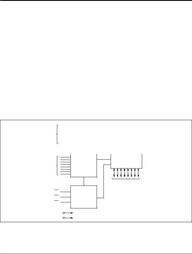
FUNCTIONAL DIAGRAM
PIN NAMES
Symbol |
Description |
|
|
A0–A16 |
Address Inputs |
I/O0–I/O7 |
Data Input/Output |
WE |
Write Enable |
|
|
CE |
Chip Enable |
|
|
OE |
Output Enable |
VCC |
+5V |
VSS |
Ground |
NC |
No Connect |
3858 PGM T01
|
|
X BUFFERS |
|
1M-BIT |
||
|
|
|
||||
|
|
|
||||
|
|
|
||||
A8–A16 |
|
LATCHES AND |
|
E2PROM |
||
|
|
|||||
|
|
|||||
|
|
DECODER |
|
ARRAY |
||
|
|
|
||||
|
|
|
|
|
|
|
|
|
|
|
|
|
|
|
|
|
|
|
|
|
|
Y BUFFERS |
I/O BUFFERS |
|
A0–A7 |
AND LATCHES |
||
LATCHES AND |
|||
|
|||
|
DECODER |
|
I/O0–I/O7
DATA INPUTS/OUTPUTS
CE |
CONTROL |
|
|
OE |
LOGIC AND |
WE |
TIMING |
|
|
VCC |
|
VSS |
|
3858 FHD F01
2
X28C010
DEVICE OPERATION
Read
Read operations are initiated by both OE and CE LOW. The read operation is terminated by either CE or OE returning HIGH. This two line control architecture eliminates bus contention in a system environment. The data bus will be in a high impedance state when either OE or CE is HIGH.
Write
Write operations are initiated when both CE and WE are LOW and OE is HIGH. The X28C010 supports both a CE and WE controlled write cycle. That is, the address is latched by the falling edge of either CE or WE, whichever occurs last. Similarly, the data is latched internally by the rising edge of either CE or WE, whichever occurs first. A byte write operation, once initiated, will automatically continue to completion, typically within 5ms.
Page Write Operation
The page write feature of the X28C010 allows the entire memory to be written in 5 seconds. Page write allows two to two hundred fifty-six bytes of data to be consecutively written to the X28C010 prior to the commencement of the internal programming cycle. The host can fetch data from another device within the system during a page write operation (change the source address), but the page address (A8 through A16) for each subsequent valid write cycle to the part during this operation must be the same as the initial page address.
The page write mode can be initiated during any write operation. Following the initial byte write cycle, the host can write an additional one to two hundred fifty six bytes in the same manner as the first byte was written. Each successive byte load cycle, started by the WE HIGH to LOW transition, must begin within 100μs of the falling edge of the preceding WE. If a subsequent WE HIGH to LOW transition is not detected within 100μs, the internal automatic programming cycle will commence. There is no page write window limitation. Effectively the page write window is infinitely wide, so long as the host continues to access the device within the byte load cycle time of 100μs.
Write Operation Status Bits
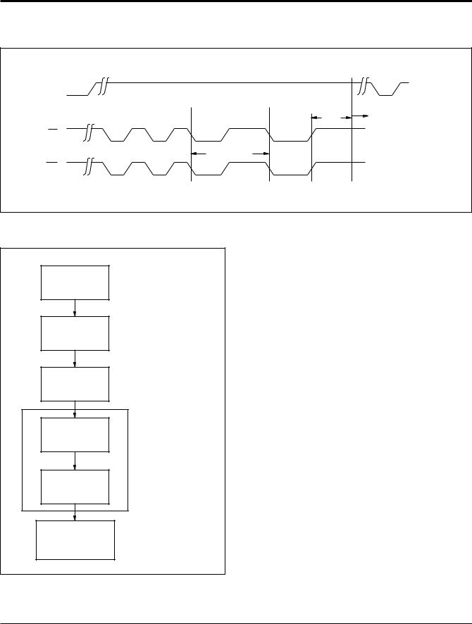
The X28C010 provides the user two write operation status bits. These can be used to optimize a system write cycle time. The status bits are mapped onto the I/O bus as shown in Figure 1.
Figure 1. Status Bit Assignment
I/O |
DP |
TB |
5 |
4 |
3 |
2 |
1 |
0 |
|
|
|
|
|
|
|
|
|
RESERVED
TOGGLE BIT
DATA POLLING
3858 FHD F11
DATA Polling (I/O7)
The X28C010 features DATA Polling as a method to indicate to the host system that the byte write or page write cycle has completed. DATA Polling allows a simple bit test operation to determine the status of the X28C010, eliminating additional interrupt inputs or external hardware. During the internal programming cycle, any attempt to read the last byte written will produce the complement of that data on I/O7 (i.e., write data = 0xxx xxxx, read data = 1xxx xxxx). Once the programming cycle is complete, I/O7 will reflect true data. Note: If the X28C010 is in the protected state and an illegal write operation is attempted DATA Polling will not operate.
Toggle Bit (I/O6)
The X28C010 also provides another method for determining when the internal write cycle is complete. During the internal programming cycle, I/O6 will toggle from HIGH to LOW and LOW to HIGH on subsequent attempts to read the device. When the internal cycle is complete the toggling will cease and the device will be accessible for additional read or write operations.
3
X28C010
DATA Polling I/O7
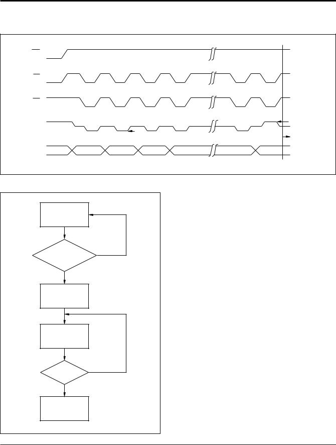
Figure 2. DATA Polling Bus Sequence
LAST
WE WRITE
CE |
|
|
|
|
|
|
|
|
OE |
|
|
|
|
|
|
|
|
|
VIH |
|
HIGH Z |
|
|
|
V |
OH |
I/O7 |
|
|
|
|
|
|||
|
|
|
VOL |
|
|
|
||
|
|
|
|
|
|
X28C010 |
||
|
|
|
|
|
|
|
READY |
|
A0–A14 |
An |
An |
An |
An |
An |
An |
An |
|
3858 FHD F12
Figure 3. DATA Polling Software Flow
WRITE DATA
WRITES NO
COMPLETE?
YES
SAVE LAST DATA
AND ADDRESS
READ LAST |
|
ADDRESS |
|
I/O7 |
NO |
COMPARE? |
|
YES |
|
X28C010 |
|
READY |
|
DATA Polling can effectively halve the time for writing to the X28C010. The timing diagram in Figure 2 illustrates the sequence of events on the bus. The software flow diagram in Figure 3 illustrates one method of implementing the routine.
3858 FHD F13
4
X28C010
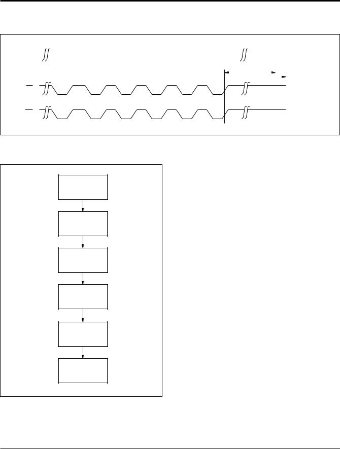
The Toggle Bit I/O6
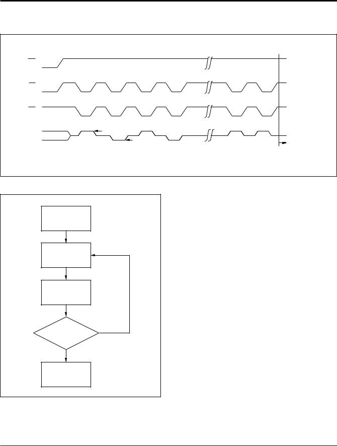
Figure 4. Toggle Bit Bus Sequence
LAST
WE WRITE
CE |
|
|
|
OE |
|
|
|
I/O6 |
* |
VOH |
HIGH Z |
VOL |
* |
||
|
|
X28C010 |
|
|
|
|
READY |
* Beginning and ending state of I/O6 will vary.
3858 FHD F14
Figure 5. Toggle Bit Software Flow
LAST WRITE
LOAD ACCUM
FROM ADDR n
COMPARE
ACCUM WITH
ADDR n
NO
COMPARE
OK?
YES
X28C010
READY
3858 FHD F15
The Toggle Bit can eliminate the software housekeeping chore of saving and fetching the last address and data written to a device in order to implement DATA Polling. This can be especially helpful in an array comprised of multiple X28C010 memories that is frequently updated. Toggle Bit Polling can also provide a method for status checking in multiprocessor applications. The timing diagram in Figure 4 illustrates the sequence of events on the bus. The software flow diagram in Figure 5 illustrates a method for polling the Toggle Bit.
5

X28C010
HARDWARE DATA PROTECTION
The X28C010 provides three hardware features that protect nonvolatile data from inadvertent writes.
•Noise Protection—A WE pulse less than 10ns will not initiate a write cycle.
•Default VCC Sense—All functions are inhibited when VCC is ≤3.5V.
•Write inhibit—Holding either OE LOW, WE HIGH, or CE HIGH will prevent an inadvertent write cycle during power-up and power-down, maintaining data integrity.
SOFTWARE DATA PROTECTION
The X28C010 offers a software controlled data protection feature. The X28C010 is shipped from Xicor with the software data protection NOT ENABLED: that is the device will be in the standard operating mode. In this mode data should be protected during power-up/-down operations through the use of external circuits. The host would then have open read and write access of the device once VCC was stable.
The X28C010 can be automatically protected during power-up and power-down without the need for external circuits by employing the software data protection feature. The internal software data protection circuit is enabled after the first write operation utilizing the software algorithm. This circuit is nonvolatile and will remain set for the life of the device unless the reset command is issued.
Once the software protection is enabled, the X28C010 is also protected from inadvertent and accidental writes in the powered-up state. That is, the software algorithm must be issued prior to writing additional data to the device.
SOFTWARE ALGORITHM
Selecting the software data protection mode requires the host system to precede data write operations by a series of three write operations to three specific addresses. Refer to Figures 6 and 7 for the sequence. The three byte sequence opens the page write window enabling the host to write from one to two hundred fiftysix bytes of data. Once the page load cycle has been completed, the device will automatically be returned to the data protected state.
6
X28C010
Software Data Protection
Figure 6. Timing Sequence—Byte or Page Write
VCC |
|
|
|
|
|
(VCC) |
|
0V |
|
|
|
|
|
|
|
DATA |
AA |
55 |
A0 |
WRITES |
tWC |
WRITE |
|
ADDR |
5555 |
2AAA |
5555 |
||||
OK |
|||||||
|
|
|
|
|
PROTECTED |
||
CE |
|
|
|
|
|
|
|
|
|
|
≤tBLC MAX |
BYTE |
|
|
|
WE |
|
|
|
OR |
|
|
|
|
|
|
PAGE |
|
|
3858 FHD F16
Figure 7. Write Sequence for
Software Data Protection
WRITE DATA AA TO ADDRESS 5555
WRITE DATA 55 TO ADDRESS 2AAA
WRITE DATA A0 TO ADDRESS 5555
WRITE DATA XX
TO ANY
ADDRESS
OPTIONAL
BYTE/PAGE
LOAD OPERATION
WRITE LAST
BYTE TO
LAST ADDRESS
AFTER tWC
RE-ENTERS DATA
PROTECTED STATE
Regardless of whether the device has previously been protected or not, once the software data protection algorithm is used and data has been written, the X28C010 will automatically disable further writes unless another command is issued to cancel it. If no further commands are issued the X28C010 will be write protected during power-down and after any subsequent power-up. The state of A15 and A16 while executing the algorithm is don’t care.
Note: Once initiated, the sequence of write operations should not be interrupted.
3858 FHD F17
7
X28C010
Resetting Software Data Protection
Figure 8. Reset Software Data Protection Timing Sequence
VCC |
|
|
|
|
|
|
|
|
|
|
|
STANDARD |
|
|
|
|
|
|
|
|
³tWC |
|
|
||
DATA |
AA |
55 |
80 |
AA |
55 |
20 |
|
|
|
|||
|
|
|
OPERATING |
|||||||||
|
|
|
||||||||||
ADDR |
5555 |
2AAA |
5555 |
5555 |
2AAA |
5555 |
|
|
|
|
MODE |
|
|
|
|
|
|||||||||
|
|
|
|
|
|
|
|
|
|
|
|
|
CE
WE
3858 FHD F18
Figure 9. Software Sequence to Deactivate Software Data Protection
WRITE DATA AA TO ADDRESS 5555
WRITE DATA 55 TO ADDRESS 2AAA
WRITE DATA 80 TO ADDRESS 5555
WRITE DATA AA TO ADDRESS 5555
WRITE DATA 55 TO ADDRESS 2AAA
WRITE DATA 20 TO ADDRESS 5555
In the event the user wants to deactivate the software data protection feature for testing or reprogramming in an E2PROM programmer, the following six step algorithm will reset the internal protection circuit. After tWC, the X28C010 will be in standard operating mode.
Note: Once initiated, the sequence of write operations should not be interrupted.
3858 FHD F19
8
 Loading...