


XICOR X25043S, X25043PI-2,7, X25043PI, X25043P, X25043P-2,7 Datasheet
...
APPLICATION NOTES
A V A I L A B L E
X25043/45AN11 • AN21
4K |
X25043/45 |
512 x 8 Bit |
Programmable Watchdog Supervisory E2PROM
FEATURES
•Programmable Watchdog Timer
•Low VCC Detection
•Reset Signal Valid to VCC = 1V
•1MHz Clock Rate
•512 X 8 Bits Serial E2PROM —4 Byte Page Mode
•Low Power CMOS
—50 μA Standby Current
—3mA Active Current
•2.7V To 5.5V Power Supply
•Block LockTM
—Protect 1/4, 1/2 or all of E 2PROM Array
•Built-in Inadvertent Write Protection —Power-Up/Power-Down protection circuitry —Write Latch
—Write Protect Pin
•High Reliability
—Endurance: 100,000 cycles per byte —Data Retention: 100 Years
—ESD protection: 2000V on all pins
•Available Packages —8-Lead PDlP —8-Lead SOIC —14-Lead TSSOP
•X25043 = Active LOW RESET
•X25045 = Active HIGH RESET
DESCRIPTION
The X25043/45 combines three popular functions, Watchdog Timer, Voltage Supervision, and E2PROM in a single package. This combination lowers the system cost and reduces the board space requirements.
The Watchdog Timer provides an independent protec-
tion system for microcontrollers. During a system failure, the X25043/45 watchdog will respond with a RESET/
RESET signal after a selectable time-out interval. The user selects the interval from three preset values. Once selected, the interval does not change, even after cycling the power.
The system is protected from low voltage conditions by the X25043/45 low VCC detection circuits. When VCC drops below the minimum VCC trip point, the system is reset. Reset is asserted until VCC returns and stabilizes.
The memory portion of the X25043/45 is a CMOS 4096bit serial E2PROM, internally organized as 512 X 8. The X25043/45 features a Serial Peripheral Interface (SPI) and software protocol allowing operation on a simple three-wire bus.
The X25043/45 utilizes Xicor’s proprietary Direct Write™ cell, providing a minimum endurance of 100,000 cycles per byte and a minimum data retention of 100 years.
DIE PHOTOGRAPH
RESET |
PROGRAMMABLE |
|
VOLTAGE |
||
CONTROL |
||
SENSOR |
||
LOGICIC |
||
|
SERIALI |
4K BITSI E2PROM |
INTERFACEI |
|
LOGICIC |
|
HIGHI |
VOLTAGE GENERATOR |
|
AND |
|
CONTROL |
Direct Write™ is a trademark of Xicor, Inc. |
|
©Xicor, Inc. 1994, 1995, 1996 Patents Pending |
1 |
3844-6.5 5/9/96 T4/C2/D2 NS |
W |
|
|
A |
T |
|
T |
||
I |
||
C |
I |
|
M |
||
H |
||
E |
||
D |
||
R |
||
O |
||
|
||
G |
|
3844 ILL F01
Characteristics subject to change without notice
X25043/45
PIN DESCRIPTIONS
Serial Output (SO)
SO is a push/pull serial data output pin. During a read cycle, data is shifted out on this pin. Data is clocked out by the falling edge of the serial clock.
Serial Input (SI)
SI is the serial data input pin. All opcodes, byte addresses, and data to be written to the memory are input on this pin. Data is latched by the rising edge of the serial clock.
Serial Clock (SCK)
The Serial Clock controls the serial bus timing for data input and output. Opcodes, addresses, or data present on the SI pin is latched on the rising edge of the clock input, while data on the SO pin changes after the falling edge of the clock input.
Chip Select (CS)
When CS is HIGH, the X25043/45 is deselected and the SO output pin is at high impedance and, unless an internal write operation is underway, the X25043/45 will be in the standby power mode. CS LOW enables the X25043/45, placing it in the active power mode. It should be noted that after power-up, a HIGH to LOW transition on CS is required prior to the start of any operation.
Write Protect (WP)
When WP is LOW, nonvolatile writes to the X25043/45 are disabled, but the part otherwise functions normally. When WP is held HIGH, all functions, including nonvolatile writes operate normally. WP going LOW while CS is still LOW will interrupt a write to the X25043/45. If the internal write cycle has already been initiated, WP going LOW will have no affect on a write.
Reset (RESET, RESET)
X25043/45, RESET/RESET is an active LOW/HIGH, open drain output which goes active whenever VCC falls below the mimimum VCC sense level. It will remain
active until VCC rises above the minimum VCC sense level for 200ms. RESET/RESET also goes active if
the Watchdog timer is enabled and CS remains either HIGH or LOW longer than the Watchdog time-out period. A falling edge of CS will reset the watchdog timer.
PIN CONFIGURATION
|
|
|
|
|
|
|
X25043/45 |
|
|
|
|
|
|
|
|
|
8-LEAD DIP/SOIC |
|
|
|
|||
|
|
|
|
|
|
|
|
|
|
|
|
|
|
|
|
1 |
8 |
|
|
|
|
||
|
|
CS |
|
|
|
|
VCC |
||||
|
|
||||||||||
|
SO |
|
2 |
7 |
|
|
|
|
|||
|
|
|
RESET/RESET |
||||||||
|
|
3 |
6 |
|
|
|
|
||||
|
WP |
|
|
|
SCK |
||||||
VSS |
|
4 |
5 |
|
SI |
||||||
|
|
||||||||||
|
|
||||||||||
|
|
|
|
|
|
|
X25043/45 |
|
|
||
|
|
|
|
|
|
14-LEAD TSSOP |
|
|
|||
|
|
|
|
|
|
|
|
|
|
|
|
|
|
|
|
|
|
|
14 |
|
|
|
|
|
CS |
|
1 |
|
|
VCC |
|
||||
|
|
||||||||||
|
13 |
|
|
||||||||
|
SO |
|
2 |
|
|
RESET/RESET |
|||||
|
|
||||||||||
|
NC |
|
3 |
12 |
|
|
NC |
||||
|
|
||||||||||
|
NC |
|
4 |
11 |
|
|
NC |
||||
|
|
||||||||||
|
NC |
|
5 |
10 |
|
|
NC |
||||
|
|
|
|
|
9 |
|
|
|
|||
|
WP |
|
6 |
|
|
SCK |
|||||
VSS |
|
7 |
8 |
|
|
SI |
|||||
|
|
|
|
|
|
|
|
|
|
3844 ILL F02.3 |
|
PIN NAMES
Symbol |
Description |
|
|
CS |
Chip Select Input |
SO |
Serial Output |
|
|
SI |
Serial Input |
|
|
SCK |
Serial Clock Input |
|
|
WP |
Write Protect Input |
|
|
VSS |
Ground |
VCC |
Supply Voltage |
RESET/RESET |
Reset Output |
3844 PGM T01.1
2

X25043/45
PRINCIPLES OF OPERATION
The X25043/45 is a 512 x 8 E2PROM designed to interface directly with the synchronous serial peripheral interface (SPI) of many popular microcontroller families.
The X25043/45 contains an 8-bit instruction register. It is accessed via the SI input, with data being clocked in on the rising SCK. CS must be LOW and WP input must be HIGH during the entire operation. The X25043/45 monitors the bus and provides a RESET/RESET output if there is no bus activity within the preset time period.
Table 1 contains a list of the instructions and their operation codes. All instructions, addresses and data are transferred MSB first. Bit 3 of the Read and Write instructions contain the higher order address bit, A8.
Data input is sampled on the first rising edge of SCK after CS goes LOW. SCK is static, allowing the user to stop the clock and then resume operations.
Write Enable Latch
The X25043/45 contains a “write enable” latch. This latch must be SET before a write operation will be completed internally. The WREN instruction will set the latch and the WRDI instruction will reset the latch. This latch is automatically reset upon a power-up condition and after the completion of a byte, page, or status register write cycle. The latch is also reset if WP is brought LOW.
Status Register
The RDSR instruction provides access to the status register. The status register may be read at any time, even during a write cycle. The status register is formatted as follows:
7 |
6 |
5 |
4 |
3 |
2 |
1 |
0 |
X |
X |
WD1 |
WD0 |
BL1 |
BL0 |
WEL |
WIP |
|
|
|
|
|
|
|
|
3844 PGM T02
When issuing, WREN, WRDI and RDSR commands, it is not necessary to send a byte address or data.
The Write-In-Process (WIP) bit indicates whether the X25043/45 is busy with a write operation. When set to a “1”, a write is in progress, when set to a “0”, no write is in progress. During a write, all other bits are set to “1”. The WIP bit is read-only.
The Write Enable Latch (WEL) bit indicates the status of the “write enable” latch. When set to a “1”, the latch is set, when set to a “0”, the latch is reset. The WEL bit is readonly and is set by the WREN instruction and reset by WRDI instruction or successful completion of a write cycle.
The Block Protect (BL0 and BL1) bits indicate the extent of protection employed. These nonvolatile bits are set by issuing the WRSR instruction and allows the user to select one of four levels of protection and program the watchdog timer. The X25043/45 is divided into four 1024-bit segments. One, two, or all four of the segments may be locked. That is, the user may read the segments but will be unable to alter (write) data within the selected segments. The partitioning is controlled as illustrated below with the state of BL1 and BL0.
Status Register Bits |
Array Addresses |
|
|
|
|
BL1 |
BL0 |
Protected |
|
|
|
0 |
0 |
None |
|
|
|
0 |
1 |
$180–$1FF |
|
|
|
1 |
0 |
$100–$1FF |
1 |
1 |
$000–$1FF |
3844 PGM T04
The Watchdog Timer (WD0 and WD1) bits allow setting of the watchdog time-out function as shown in the table below. These nonvolatile bits are set by issuing the WRSR instruction.
Status Register Bits |
Watchdog Time-out |
|
|
|
|
WD1 |
WD0 |
(Typical) |
|
|
|
0 |
0 |
1.4 Seconds |
|
|
|
0 |
1 |
600 Milliseconds |
|
|
|
1 |
0 |
200 Milliseconds |
1 |
1 |
Disabled |
|
|
|
3844 PGM T03
3

X25043/45
Clock and Data Timing
Data input on the SI line is latched on the rising edge of SCK. Data is output on the SO line by the falling edge of SCK.
Read Sequence
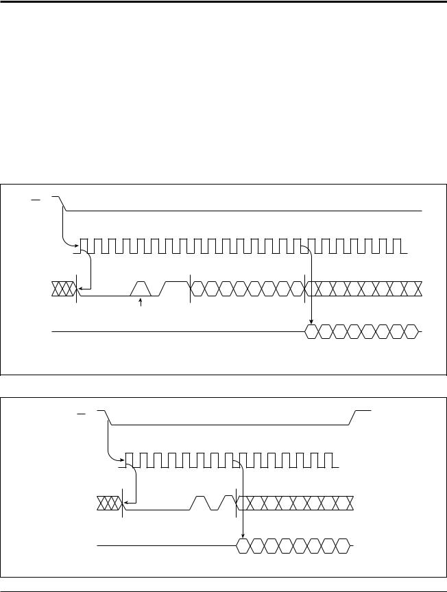
When reading from the E2PROM memory array, CS is first pulled LOW to select the device. The 8-bit READ instruction is transmitted to the X25043/45, followed by the 8-bit byte address. Bit 3 of the Read instruction contains address A8. This bit is used to select the upper or lower half of the device. After the read opcode and byte address are sent, the data stored in the memory at the selected address is shifted out on the SO line. The data stored in memory at the next address can be read sequentially by continuing to provide clock pulses. The byte address is automatically incremented to the next higher address after each byte of data is shifted out. When the highest address is reached ($1FF) the address counter rolls over to address $000, allowing the read cycle to be continued indefinitely. The read operation is terminated by taking CS HIGH. Refer to the read E2PROM Array operation sequence illustrated in Figure 1.
To read the status register the CS line is first pulled LOW to select the device followed by the 8-bit RDSR instruction. After the read status register opcode is sent, the contents of the status register is shifted out on the SO line as shown in Figure 2.
Write Sequence
Prior to any attempt to write data into the X25043/45 the “write enable” latch must first be set by issuing the WREN instruction (See Figure 3). CS is first taken LOW, then the WREN instruction is clocked into the X25043/45. After all eight bits of the instruction are
Table 1. Instruction Set
transmitted, CS must then be taken HIGH. If the user continues the write operation without taking CS HIGH after issuing the WREN instruction the write operation will be ignored.
To write data to the E2PROM memory array, the user issues the WRITE instruction, followed by the address and then the data to be written. Bit 3 of the Write instruction contains address A8. This bit is used to select the upper or lower half of the device. This is minimally a twenty-four clock operation. CS must go LOW and remain LOW for the duration of the operation. The host may continue to write up to four bytes of data to the X25043/45. The only restriction is the four bytes must reside on the same page. A page address begins with address X XXXX XX00 and ends with X XXXX XX11. If the byte address counter reaches X XXXX XX11 and the clock continues the counter will roll back to the first address of the page and overwrite any data that may have been written.
For the write operation (byte or page write) to be completed, CS can only be brought HIGH after the twenty-fourth, thirty-second, fortieth, or forty-eighth clock. If it is brought HIGH at any other time, the write operation will not be completed. Refer to Figure 4 and 5 below for a detailed illustration of the write sequences.
While the write is in progress, following a status register or E2PROM write sequence the status register may be read to check the WIP bit. During this time the WIP bit will be HIGH and all other bits in the status register will be undefined.
RESET/RESET Operation
The RESET (X25043) output is designed to go LOW whenever VCC has dropped below the minimum trip point and/or the Watchdog timer has reached its programmable time-out limit.
Instruction Name |
Instruction Format* |
Operation |
|
|
|
|
|
WREN |
0000 |
0110 |
Set the Write Enable Latch (Enable Write Operations) |
|
|
|
|
WRDI |
0000 |
0100 |
Reset the Write Enable Latch (Disable Write Operations) |
RDSR |
0000 0101 |
Read Status Register |
|
|
|
|
|
WRSR |
0000 0001 |
Write Status Register (Block Lock Bits) |
|
|
|
|
|
READ |
0000 |
A8011 |
Read Data from Memory Array beginning at selected |
address |
|||
WRITE |
0000 |
A8010 |
Write Data to Memory Array beginning at Selected Address |
(1 to 4 Bytes) |
|||
|
|
|
|
3844 PGM T05.1
*Instructions are shown MSB in leftmost position. Instructions are transferred MSB first.
4
X25043/45
The RESET (X25045) output is designed to go HIGH whenever VCC has dropped below the minimum trip point and/or the watchdog timer has reached its programmable time-out limit.
Operational Notes
The X25043/45 powers-up in the following state:
•The device is in the low power standby state.
•A HIGH to LOW transition on CS is required to enter an active state and receive an instruction.
•SO pin is high impedance.
•The “write enable” latch is reset.
Figure 1. Read E2PROM Array Operation Sequence
Data Protection
The following circuitry has been included to prevent inadvertent writes:
•The “write enable” latch is reset upon power-up.
•A WREN instruction must be issued to set the “write enable” latch.
•CS must come HIGH at the proper clock count in order to start a write cycle.
The “write enable” latch is reset when WP is brought LOW.
CS |
|
|
|
|
|
|
|
|
|
|
|
|
|
|
|
|
|
|
|
|
|
|
|
0 |
1 |
2 |
3 |
4 |
5 |
6 |
7 |
8 |
9 |
10 |
11 |
12 |
13 |
14 |
15 |
16 |
17 |
18 |
19 |
20 |
21 |
22 |
|
SCK |
|
|
|
|
|
|
|
|
|
|
|
|
|
|
|
|
|
|
|
|
|
|
|
|
INSTRUCTION |
|
|
|
|
|
BYTE ADDRESS |
|
|
|
|
|
|
|
|
|
|
||||||
SI |
|
|
|
8 |
|
|
|
7 |
6 |
5 |
4 |
3 |
2 |
1 |
0 |
|
|
|
|
|
|
|
|
|
|
|
|
9TH BIT OF ADDRESS |
|
|
|
|
|
|
|
|
DATA OUT |
|
|
|
|||||||
HIGH IMPEDANCE |
|
|
|
|
|
|
|
|
|
|
|
|
|
|
|
|
|
|
|||||
|
|
|
|
|
|
|
|
|
|
|
|
|
7 |
6 |
5 |
4 |
3 |
2 |
1 |
0 |
|||
SO |
|
|
|
|
|
|
|
|
|
|
|
|
|
|
|
||||||||
|
|
|
|
|
|
|
|
|
|
|
|
|
|
|
|
MSB |
|
|
|
|
|
|
|
|
|
|
|
|
|
|
|
|
|
|
|
|
|
|
|
|
|
|
|
|
|
3844 FHD F04 |
|
Figure 2. Read Status Register Operation Sequence
CS
0 |
1 |
2 |
3 |
4 |
5 |
6 |
7 |
8 |
9 |
10 |
11 |
12 |
13 |
14 |
SCK
INSTRUCTION
SI
DATA OUT
HIGH IMPEDANCE
SO 7 6 5 4 3 2 1 0
MSB
3844 ILL F15
5
 Loading...