


XICOR X24C04S8-3, X24C04S8-2,7, X24C04S8, X24C04S14M-3,5, X24C04S14M-3 Datasheet
...
X24C04
4K |
X24C04 |
512 x 8 Bit |
Serial E2PROM
FEATURES
•2.7V to 5.5V Power Supply
•Low Power CMOS
—Active Read Current Less Than 1 mA —Active Write Current Less Than 3 mA
—Standby Current Less Than 50 μA
•Internally Organized 512 x 8
•2 Wire Serial Interface
—Bidirectional Data Transfer Protocol
•Sixteen Byte Page Write Mode —Minimizes Total Write Time Per Byte
•Self Timed Write Cycle
—Typical Write Cycle Time of 5 ms
•High Reliability —Endurance: 100,000 Cycles —Data Retention: 100 Years
•8 Pin Mini-DIP, 8 Pin SOIC and 14 Pin SOIC Packages
DESCRIPTION
The X24C04 is a CMOS 4096 bit serial E2PROM, internally organized 512 x 8. The X24C04 features a serial interface and software protocol allowing operation on a simple two wire bus.
The X24C04 is fabricated with Xicor’s advanced CMOS Textured Poly Floating Gate Technology.
The X24C04 utilizes Xicor’s proprietary DirectWrite™ cell providing a minimum endurance of 100,000 cycles and a minimum data retention of 100 years.
FUNCTIONAL DIAGRAM
(8) |
VCC |
|
|
|
|
|
|
|
|
|
|
|
|
|
|
|
|
|
|||
(4) |
VSS |
|
|
|
|
|
|
|
|
|
|
|
|
|
|
|
|
|
|||
(7) |
TEST |
|
|
|
|
START CYCLE |
|
H.V. GENERATION |
||
|
|
|
|
|
||||||
|
|
|
|
|
|
|
|
|
||
|
|
|
|
|
|
|
|
|
TIMING |
|
|
|
|
|
|
|
|
|
|
|
|
|
|
|
|
|
|
|
|
|
|
|
|
|
|
|
|
|
|
|
|
|
& CONTROL |
|
|
|
|
|
|
|
|
|
||
(5) SDA |
START |
|
|
|
|
|
|
STOP |
|
|
|
|
|
|
LOGIC |
|
|
|
|
|
|
|
|
CONTROL |
|
|
|
|
|
|
LOGIC |
|
|
|
|
SLAVE ADDRESS |
|
|
|
|
E2PROM |
|
REGISTER |
|
|
XDEC |
|
|
(6) SCL |
LOAD |
INC |
|
32 X 128 |
||
+COMPARATOR |
|
|
||||
(3) A2 |
|
WORD |
|
|
|
|
(2) A1 |
|
ADDRESS |
|
|
|
|
|
COUNTER |
|
|
|
||
(1) A0 |
|
|
|
|
||
|
|
|
|
|
|
|
|
|
R/W |
|
|
|
YDEC |
|
|
|
|
|
|
8 |
|
|
|
PIN |
|
CK |
DOUT |
|
|
|
|
|
||
|
|
|
|
|
DATA REGISTER |
|
|
DOUT |
|
|
|
|
|
|
ACK |
|
|
|
|
3839 FHD F01 |
|
|
|
|
|
|
|
DirectWrite™ is a trademark of Xicor, Inc.
© Xicor, 1991 Patents Pending |
1 |
Characteristics subject to change without notice |
|
|
3839-1

X24C04
PIN DESCRIPTIONS
Serial Clock (SCL)
The SCL input is used to clock all data into and out of the device.
Serial Data (SDA)
SDA is a bidirectional pin used to transfer data into and out of the device. It is an open drain output and may be wire-ORed with any number of open drain or open collector outputs.
An open drain output requires the use of a pull-up resistor. For selecting typical values, refer to the Pull-Up Resistor selection graph at the end of this data sheet.
Address (A0)
A0 is unused by the X24C04, however, it must be tied to VSS to insure proper device operation.
Address (A1, A2)
The Address inputs are used to set the appropriate bits of the seven bit slave address. These inputs can be used static or actively driven. If used statically they must be tied to VSS or VCC as appropriate. If driven they must be driven to VSS or to VCC.
PIN NAMES
Symbol |
Description |
|
|
A0–A2 |
Address Inputs |
SDA |
Serial Data |
|
|
SCL |
Serial Clock |
|
|
TEST |
Hold at VSS |
VSS |
Ground |
VCC |
Supply Voltage |
NC |
No Connect |
|
|
3839 PGM T01
PIN CONFIGURATION
DIP/SOIC
A0 |
|
1 |
8 |
VCC |
|
||||
|
||||
A1 |
|
2 |
7 |
TEST |
|
||||
|
|
|
X24C04 |
|
A2 |
|
3 |
6 |
SCL |
|
||||
VSS |
|
4 |
5 |
SDA |
|
3839 FHD F02
SOIC
NC |
|
|
|
|
1 |
14 |
|
|
|
|
NC |
A0 |
|
|
|
|
2 |
13 |
|
|
|
|
VCC |
|
|
|
|
|
|
|
|
||||
A1 |
|
|
|
|
3 |
12 |
|
|
|
|
TEST |
|
|
|
|
|
|
|
|
||||
NC |
|
|
|
|
4 |
X24C04 11 |
|
|
|
|
NC |
A2 |
|
|
|
|
5 |
10 |
|
|
|
|
SCL |
|
|
|
|
|
|
|
|
||||
VSS |
|
|
|
|
6 |
9 |
|
|
|
|
SDA |
|
|
|
|
|
|
|
|
||||
NC |
|
|
|
|
7 |
8 |
|
|
|
|
NC |
|
|
|
|
|
|
|
|
|
|
|
|
3839 FHD F03
2
X24C04
DEVICE OPERATION
The X24C04 supports a bidirectional bus oriented protocol. The protocol defines any device that sends data onto the bus as a transmitter, and the receiving device as the receiver. The device controlling the transfer is a master and the device being controlled is the slave. The master will always initiate data transfers, and provide the clock for both transmit and receive operations. Therefore, the X24C04 will be considered a slave in all applications.
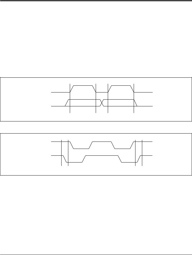
Figure 1. Data Validity
Clock and Data Conventions
Data states on the SDA line can change only during SCL LOW. SDA state changes during SCL HIGH are reserved for indicating start and stop conditions. Refer to Figures 1 and 2.
Start Condition
All commands are preceded by the start condition, which is a HIGH to LOW transition of SDA when SCL is HIGH. The X24C04 continuously monitors the SDA and SCL lines for the start condition and will not respond to any command until this condition has been met.
SCL
SDA
DATA STABLE DATA
CHANGE 3839 FHD F06
Figure 2. Definition of Start and Stop
SCL
SDA
START BIT |
STOP BIT |
3839 FHD F07
3
X24C04
Stop Condition
All communications must be terminated by a stop condition, which is a LOW to HIGH transition of SDA when SCL is HIGH. The stop condition is also used by the X24C04 to place the device in the standby power mode after a read sequence. A stop condition can only be issued after the transmitting device has released the bus.
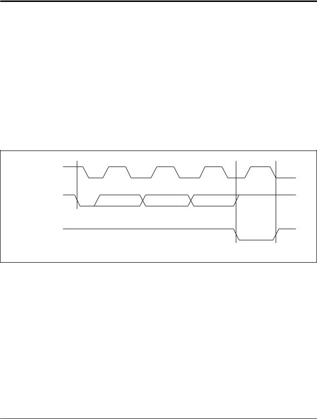
Acknowledge
Acknowledge is a software convention used to indicate successful data transfer. The transmitting device, either master or slave, will release the bus after transmitting eight bits. During the ninth clock cycle the receiver will pull the SDA line LOW to acknowledge that it received the eight bits of data. Refer to Figure 3.
Figure 3. Acknowledge Response From Receiver
The X24C04 will respond with an acknowledge after recognition of a start condition and its slave address. If both the device and a write operation have been selected, the X24C04 will respond with an acknowledge after the receipt of each subsequent eight bit word.
In the read mode the X24C04 will transmit eight bits of data, release the SDA line and monitor the line for an acknowledge. If an acknowledge is detected and no stop condition is generated by the master, the X24C04 will continue to transmit data. If an acknowledge is not detected, the X24C04 will terminate further data transmissions. The master must then issue a stop condition to return the X24C04 to the standby power mode and place the device into a known state.
SCL FROM |
|
|
|
MASTER |
1 |
8 |
9 |
DATA
OUTPUT
FROM
TRANSMITTER
DATA
OUTPUT
FROM
RECEIVER
START |
ACKNOWLEDGE |
3839 FHD F08
4
X24C04
DEVICE ADDRESSING
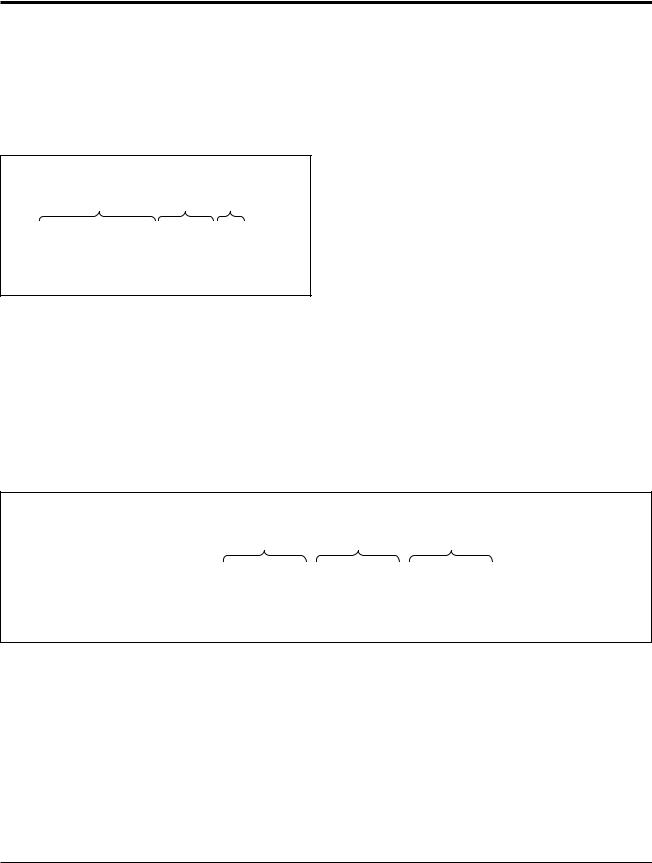
Following a start condition the master must output the address of the slave it is accessing. The most significant four bits of the slave are the device type identifier (see Figure 4). For the X24C04 this is fixed as 1010[B].
Figure 4. Slave Address
|
|
|
|
|
|
|
|
HIGH |
|||
|
|
|
|
|
|
|
|
ORDER |
|||
|
DEVICE TYPE |
|
DEVICE |
WORD |
|||||||
|
|
IDENTIFIER |
|
ADDRESS ADDRESS |
|||||||
|
|
|
|
|
|
|
|
|
|
|
|
|
|
|
|
|
|
|
|
|
|
|
|
1 |
|
0 |
1 |
|
0 |
A2 |
A1 |
A0 |
R/W |
||
|
|
|
|
|
|
|
|
|
|
|
|
3839 FHD F09
The next two significant bits address a particular device. A system could have up to four X24C04 devices on the bus (see Figure 10). The four addresses are defined by the state of the A1 and A2 inputs.
The next bit of the slave address is an extension of the array’s address and is concatenated with the eight bits of address in the word address field, providing direct access to the whole 512 x 8 array.
Figure 5. Byte Write
The last bit of the slave address defines the operation to be performed. When set to one a read operation is selected, when set to zero a write operation is selected.
Following the start condition, the X24C04 monitors the SDA bus comparing the slave address being transmitted with its slave address (device type and state of A1 and A2 inputs). Upon a correct compare the X24C04 outputs an acknowledge on the SDA line. Depending on the state of the R/W bit, the X24C04 will execute a read or write operation.
WRITE OPERATIONS
Byte Write
For a write operation, the X24C04 requires a second address field. This address field is the word address, comprised of eight bits, providing access to any one of the 512 words of memory. Upon receipt of the word address the X24C04 responds with an acknowledge, and awaits the next eight bits of data, again responding with an acknowledge. The master then terminates the transfer by generating a stop condition, at which time the X24C04 begins the internal write cycle to the nonvolatile memory. While the internal write cycle is in progress the X24C04 inputs are disabled, and the device will not respond to any requests from the master. Refer to Figure 5 for the address, acknowledge and data transfer sequence.
|
S |
|
|
|
|
|
|
|
|
|
|
|
|
|
|
|
|
|
|
|
|
|
|
|
|
|
|
|
|
|
|
T |
|
SLAVE |
|
|
|
|
WORD |
|
|
|
|
|
|
|
|
|
|
S |
|
||||||||||
BUS ACTIVITY: A |
|
|
|
|
|
|
|
|
|
|
|
|
|
|
|
T |
|
|||||||||||||
ADDRESS |
|
|
|
ADDRESS |
|
|
|
DATA |
|
|||||||||||||||||||||
MASTER |
R |
|
|
|
|
|
|
|
|
|
|
|
|
|
|
|
|
|
|
|
|
|
|
|
|
|
|
O |
|
|
|
T |
|
|
|
|
|
|
|
|
|
|
|
|
|
|
|
|
|
|
|
|
|
|
|
|
|
|
P |
|
|
SDA LINE |
S |
|
|
|
|
|
|
|
|
|
|
|
|
|
|
|
|
|
|
|
|
|
|
|
|
|
|
|
P |
|
|
|
|
|
|
|
|
|
|
|
|
|
|
|
|
|
|
|
|
|
|
|
|
|
|
|
|
|
|||
|
|
|
|
|
|
|
|
|
|
|
|
|
|
|
|
|
|
|
|
|
|
|
|
|
|
|
|
|
|
|
BUS ACTIVITY: |
A |
A |
A |
C |
C |
C |
|
X24C04 |
K |
K |
K |
3839 FHD F10
5
X24C04
Page Write
The X24C04 is capable of a sixteen byte page write operation. It is initiated in the same manner as the byte write operation, but instead of terminating the write cycle after the first data word is transferred, the master can transmit up to fifteen more words. After the receipt of each word, the X24C04 will respond with an acknowledge.
After the receipt of each word, the four low order address bits are internally incremented by one. The high order five bits of the address remain constant. If the master should transmit more than sixteen words prior to generating the stop condition, the address counter will “roll over” and the previously written data will be overwritten. As with the byte write operation, all inputs are disabled until completion of the internal write cycle. Refer to Figure 6 for the address, acknowledge and data transfer sequence.
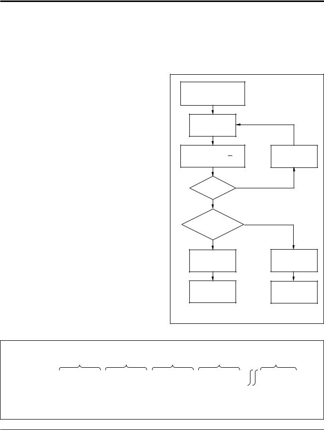
Acknowledge Polling
The disabling of the inputs can be used to take advantage of the typical 5 ms write cycle time. Once the stop condition is issued to indicate the end of the host’s write operation the X24C04 initiates the internal write cycle. ACK polling can be initiated immediately. This involves issuing the start condition followed by the slave address for a write operation. If the X24C04 is still busy with the write operation no ACK will be returned. If the X24C04 has completed the write operation an ACK will be returned and the host can then proceed with the next read or write operation. Refer to Flow 1.
READ OPERATIONS
Read operations are initiated in the same manner as write operations with the exception that the R/W bit of the slave address is set to a one. There are three basic read operations: current address read, random read and sequential read.
It should be noted that the ninth clock cycle of the read operation is not a “don’t care.” To terminate a read operation, the master must either issue a stop condition during the ninth cycle or hold SDA HIGH during the ninth clock cycle and then issue a stop condition.
Flow 1. ACK Polling Sequence
WRITE OPERATION |
|
|
|
COMPLETED |
|
|
|
ENTER ACK POLLING |
|
|
|
ISSUE |
|
|
|
START |
|
|
|
ISSUE SLAVE |
|
|
ISSUE STOP |
ADDRESS AND R/W = 0 |
|
||
|
|
||
ACK |
NO |
|
|
RETURNED? |
|
||
|
|
|
|
YES |
|
|
|
NEXT |
|
NO |
|
OPERATION |
|
|
|
|
|
|
|
A WRITE? |
|
|
|
YES |
|
|
|
ISSUE BYTE |
|
|
ISSUE STOP |
ADDRESS |
|
|
|
|
|
|
|
PROCEED |
|
|
PROCEED |
|
|
|
3839 FHD F12 |
Figure 6. Page Write
|
S |
|
|
|
|
|
|
|
|
|
|
|
|
|
|
|
|
|
|
|
|
|
|
|
|
|
|
|
|
|
|
|
|
|
|
|
|
|
|
|
|
|
|
|
|
|
|
|
|
T |
|
SLAVE |
|
|
|
|
WORD |
|
|
|
|
|
|
|
|
|
|
|
|
|
|
|
|
|
|
|
|
|
|
|
|
|
|
|
|
|
S |
||||||||||
BUS ACTIVITY: A |
|
|
|
|
|
|
|
|
|
|
|
|
|
|
|
|
|
|
|
|
|
|
|
|
|
|
|
|
|
|
|
|
|
|
T |
|||||||||||||
ADDRESS |
|
|
ADDRESS (n) |
|
|
|
DATA n |
|
|
DATA n+1 |
|
|
|
DATA n+15 |
|
|||||||||||||||||||||||||||||||||
MASTER |
R |
|
|
|
|
|
|
|
|
|
|
|
|
|
|
|
|
|
|
|
|
|
|
|
|
|
|
|
|
|
|
|
|
|
|
|
|
|
|
|
|
|
|
|
|
|
O |
|
|
T |
|
|
|
|
|
|
|
|
|
|
|
|
|
|
|
|
|
|
|
|
|
|
|
|
|
|
|
|
|
|
|
|
|
|
|
|
|
|
|
|
|
|
|
|
|
P |
|
SDA LINE |
S |
|
|
|
|
|
|
|
|
|
|
|
|
|
|
|
|
|
|
|
|
|
|
|
|
|
|
|
|
|
|
|
|
|
|
|
|
|
|
|
|
|
|
|
|
|
|
P |
|
|
|
|
|
|
|
|
|
|
|
|
|
|
|
|
|
|
|
|
|
|
|
|
|
|
|
|
|
|
|
|
|
|
|
|
|
|
|
|
|
|
|
|
|
||||
|
|
|
|
|
|
|
|
|
|
|
|
|
|
|
|
|
|
|
|
|
|
|
|
|
|
|
|
|
|
|
|
|
|
|
|
|
|
|
|
|
|
|
|
|
|
|
|
|
BUS ACTIVITY: |
A |
A |
A |
A |
A |
C |
C |
C |
C |
C |
|
X24C04 |
K |
K |
K |
K |
K |
|
|
NOTE: In this example n = xxxx 000 (B); x = 1 or 0 |
|
3839 FHD F11 |
|
6
 Loading...