


XICOR X24C01MM-3, X24C01MM-2,7, X24C01MM, X24C01MI-3,5, X24C01MI-3 Datasheet
...
PreliminaryX24C01 Information
1K |
X24C01 |
128 x 8 Bit |
Serial E2PROM
FEATURES
•2.7V to 5.5V Power Supply
•Low Power CMOS
—Active Current Less Than 1 mA
—Standby Current Less Than 50 μA
•Internally Organized 128 x 8
•2 Wire Serial Interface
—Bidirectional Data Transfer Protocol
•Four Byte Page Write Mode
•Self Timed Write Cycle
—Typical Write Cycle Time of 5 ms
•High Reliability —Endurance: 100,000 Cycles —Data Retention: 100 Years
•8-Pin Mini-DIP, 8-PIN MSOP, and 8-PIN SOIC Packages
DESCRIPTION
The X24C01 is a CMOS 1024 bit serial E2PROM, internally organized as 128 x 8. The X24C01 features a serial interface and software protocol allowing operation on a simple two wire bus.
Xicor E2PROMs are designed and tested for applications requiring extended endurance. Inherent data retention is greater than 100 years.
FUNCTIONAL DIAGRAM
(8) |
VCC |
|
|
|
|
|
|
|
|
|
|
|
|||
(4) |
VSS |
|
|
|
|
START CYCLE |
H.V. GENERATION |
|
|
|
|||||
|
|
|
|
|
|
|
TIMING |
|
|
|
|
|
|
|
|
|
|
|
|
|
|
|
& CONTROL |
(5) SDA |
START |
|
|
||||
|
|
|
|||||
|
|
|
|||||
|
|
|
|
STOP |
|
|
|
|
|
|
|
LOGIC |
|
|
|
|
|
|
|
|
|
|
|
(6) SCL
DOUT
ACK
|
CONTROL |
|
|
|
|
LOGIC |
|
|
|
|
|
XDEC |
|
E2PROM |
LOAD |
INC |
|
32 X 32 |
|
|
|
|||
WORD |
|
|
|
|
ADDRESS |
|
|
|
|
COUNTER |
|
|
|
|
R/W |
|
|
|
YDEC |
|
|
|
|
8 |
|
PIN |
|
CK |
DOUT |
|
|
|
||
|
|
|
DATA REGISTER |
|
3837 FHD F01
© Xicor, 1991 Patents Pending |
1 |
Characteristics subject to change without notice |
|
|
3837-1.2 7/28/97 T1/C0/D0 SH
X24C01
PIN DESCRIPTIONS
Serial Clock (SCL)
The SCL input is used to clock all data into and out of the device.
Serial Data (SDA)
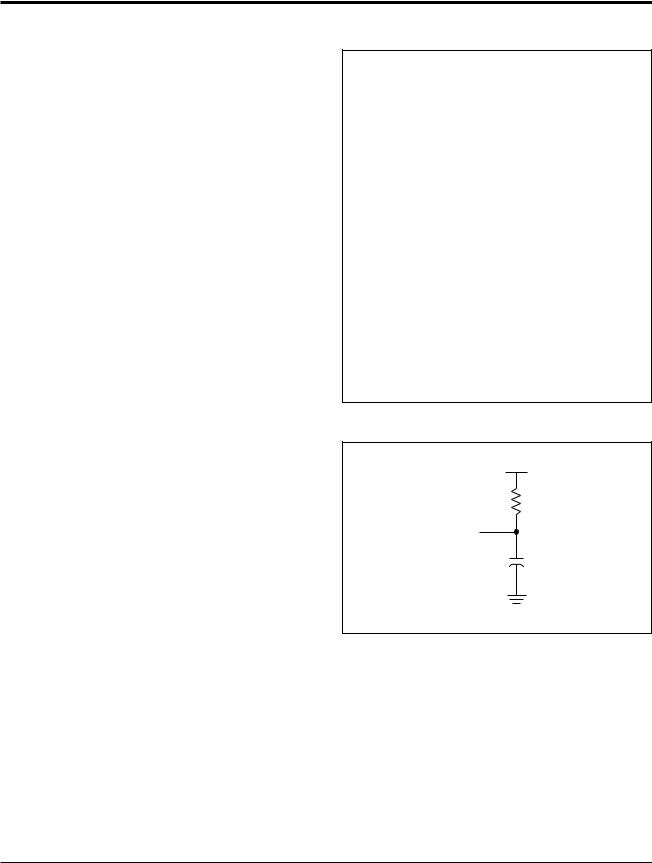
SDA is a bidirectional pin used to transfer data into and out of the device. It is an open drain output and may be wire-ORed with any number of open drain or open collector outputs.
An open drain output requires the use of a pull-up resistor. For selecting typical values, refer to the Guidelines for Calculating Typical Values of Bus Pull-Up Resistors graph.
PIN NAMES
Symbol |
|
Description |
|
|
|
NC |
|
No Connect |
|
|
|
VSS |
|
Ground |
VCC |
|
Supply Voltage |
SDA |
|
Serial Data |
|
|
|
SCL |
|
Serial Clock |
|
|
3837 PGM T01 |
A.C. CONDITIONS OF TEST |
||
|
|
|
Input Pulse Levels |
|
VCC x 0.1 to VCC x 0.9 |
Input Rise and |
|
|
Fall Times |
|
10 ns |
|
|
|
Input and Output |
|
|
Timing Levels |
|
VCC x 0.5 |
|
|
3837 PGM T02 |
PIN CONFIGURATION
|
|
|
PLASTICDIP |
|
|
|
|
|
|
|
|
|
|
|
|
|
|
NC |
|
1 |
8 |
|
VCC |
|
|
||||
|
|
||||
NC |
|
2 |
7 |
|
NC |
|
|
|
X24C01 |
|
|
NC |
|
3 |
6 |
|
SCL |
VSS |
|
4 |
5 |
|
SDA |
|
|
||||
|
|
3837 FHD F02
|
|
|
|
|
|
SOIC/MSOP |
|
|
|
|
|
|
|
|
|
|
|
|
|
|
|
|
|
NC |
|
|
|
|
1 |
8 |
|
|
|
|
VCC |
|
|
|
|
|
|
|
|
||||
NC |
|
|
|
2 |
7 |
|
|
|
|
NC |
|
|
|
|
|
|
|
X24C01 |
|
|
|
|
|
NC |
|
|
|
|
3 |
6 |
|
|
|
|
SCL |
VSS |
|
|
|
|
4 |
5 |
|
|
|
|
SDA |
|
|
|
|
|
|
|
|||||
|
|
|
|
|
|
|
|
|
|
|
|
3837 FHD F03
EQUIVALENT A.C. LOAD CIRCUIT
5V
2190Ω
OUTPUT
100pF
3837 FHD F16
2
X24C01
DEVICE OPERATION
The X24C01 supports a bidirectional bus oriented protocol. The protocol defines any device that sends data onto the bus as a transmitter and the receiving device as the receiver. The device controlling the transfer is a master and the device being controlled is the slave. The master will always initiate data transfers and provide the clock for both transmit and receive operations. Therefore, the X24C01 will be considered a slave in all applications.
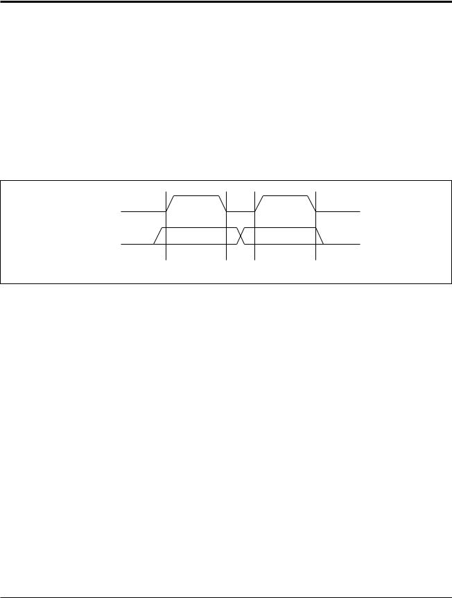
Figure 1. Data Validity
Clock and Data Conventions
Data states on the SDA line can change only during SCL LOW. SDA state changes during SCL HIGH are reserved for indicating start and stop conditions. Refer to Figures 1 and 2.
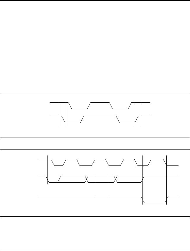
Start Condition
All commands are preceded by the start condition, which is a HIGH to LOW transition of SDA when SCL is HIGH. The X24C01 continuously monitors the SDA and SCL lines for the start condition and will not respond to any command until this condition has been met.
SCL
SDA
DATA STABLE DATA CHANGE
3837 FHD F06
3
X24C01
Stop Condition
All communications must be terminated by a stop condition, which is a LOW to HIGH transition of SDA when SCL is HIGH. The stop condition is also used by the X24C01 to place the device in the standby power mode after a read sequence. A stop condition can only be issued after the transmitting device has released the bus.
Acknowledge
Acknowledge is a software convention used to indicate successful data transfers. The transmitting device will release the bus after transmitting eight bits. During the ninth clock cycle the receiver will pull the SDA line LOW to acknowledge that it received the eight bits of data. Refer to Figure 3.
Figure 2. Definition of Start and Stop
The X24C01 will respond with an acknowledge after recognition of a start condition, a seven bit word address and a R/W bit. If a write operation has been selected, the X24C01 will respond with an acknowledge after each byte of data is received.
In the read mode the X24C01 will transmit eight bits of data, release the SDA line and monitor the line for an acknowledge. If an acknowledge is detected and no stop condition is generated by the master, the X24C01 will continue to transmit data. If an acknowledge is not detected, the X24C01 will terminate further data transmissions. The master must then issue a stop condition to return the X24C01 to the standby power mode and place the device into a known state.
|
SCL |
|
|
|
SDA |
|
|
|
START CONDITION |
STOP CONDITION |
|
|
|
|
3837 FHD F07 |
Figure 3. Acknowledge Response From Receiver |
|
|
|
SCL FROM |
|
|
|
MASTER |
1 |
8 |
9 |
DATA
OUTPUT
FROM
TRANSMITTER
DATA
OUTPUT
FROM
RECEIVER
START |
ACKNOWLEDGE |
3837 FHD F08
4
X24C01
WRITE OPERATIONS
Byte Write
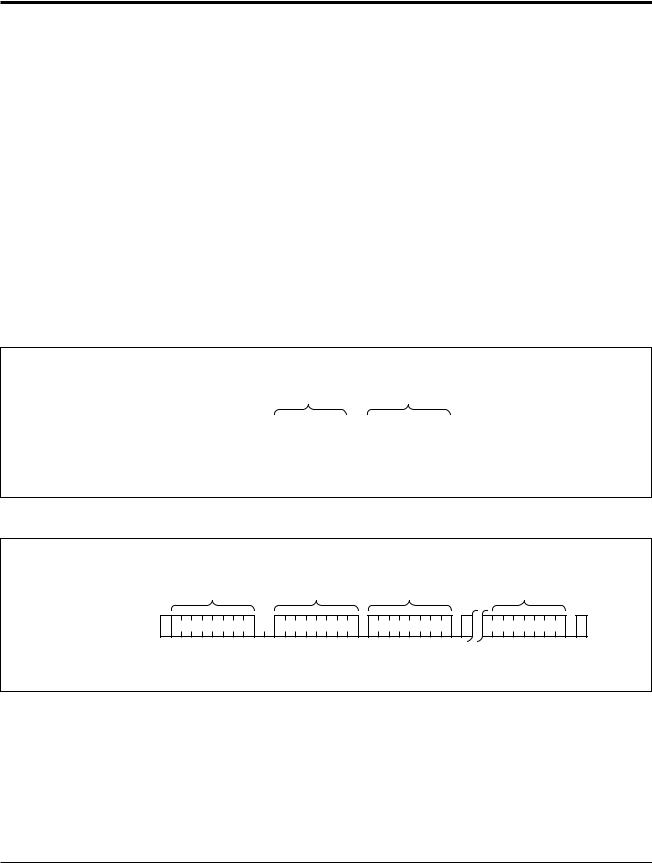
To initiate a write operation, the master sends a start condition followed by a seven bit word address and a write bit. The X24C01 responds with an acknowledge, then waits for eight bits of data and then responds with an acknowledge. The master then terminates the transfer by generating a stop condition, at which time the X24C01 begins the internal write cycle to the nonvolatile memory. While the internal write cycle is in progress, the X24C01 inputs are disabled, and the device will not respond to any requests from the master. Refer to Figure 4 for the address, acknowledge and data transfer sequence.
Page Write
The most significant five bits of the word address define
Figure 4. Byte Write
the page address. The X24C01 is capable of a four byte page write operation. It is initiated in the same manner as the byte write operation, but instead of terminating the transfer of data after the first data byte, the master can transmit up to three more bytes. After the receipt of each data byte, the X24C01 will respond with an acknowledge.
After the receipt of each data byte, the two low order address bits are internally incremented by one. The high order five bits of the address remain constant. If the master should transmit more than four data bytes prior to generating the stop condition, the address counter will “roll over” and the previously transmitted data will be overwritten. As with the byte write operation, all inputs are disabled until completion of the internal write cycle. Refer to Figure 5 for the address, acknowledge and data transfer sequence.
BUS ACTIVITY:
SDA LINE
BUS ACTIVITY: X24C01
S |
|
|
|
|
|
|
|
|
|
|
|
|
|
|
|
|
|
|
|
|
T |
|
WORD |
|
|
|
|
|
|
|
|
|
|
|
S |
||||||
A |
ADDRESS (n) |
|
|
|
|
DATA n |
T |
|||||||||||||
R |
|
|
|
|
O |
|||||||||||||||
T |
|
|
|
|
|
|
|
|
|
|
|
|
|
|
|
|
|
|
P |
|
S |
|
|
|
|
|
|
|
|
|
|
|
|
|
|
|
|
|
|
P |
|
|
|
|
|
|
|
|
|
|
|
|
|
|
|
|
|
|
|
|
||
|
|
|
|
|
|
|
|
|
|
|
|
|
|
|
|
|
|
|
|
|
M |
L R A |
A |
||
S |
S / C |
C |
||
B |
B |
W |
K |
K |
3837 FHD F09
Figure 5. Page Write
BUS ACTIVITY:
SDA LINE
BUS ACTIVITY: X24C01
S |
|
|
|
|
|
|
T |
WORD |
|
|
|
S |
|
A |
|
|
|
T |
||
ADDRESS (n) |
DATA n |
DATA n+1 |
DATA n+3 |
|||
R |
O |
|||||
T |
|
|
|
|
P |
|
S |
|
|
|
|
P |
M |
L R A |
A |
A |
A |
||
S |
S / C |
C |
C |
C |
||
B |
B |
|
K |
K |
K |
K |
W |
||||||
|
|
|
|
|
|
3837 FHD F10 |
5
 Loading...