


XICOR X20C04P, X20C04JM-25, X20C04JM-20, X20C04JM-15, X20C04JM Datasheet
...
X20C04
4K |
X20C04 |
512 x 8 Bit |
Nonvolatile Static RAM
FEATURES
•High Reliability
—Endurance: 1,000,000 Nonvolatile Store Operations
—Retention: 100 Years Minimum
•Power-on Recall
—E 2PROM Data Automatically Recalled Into SRAM Upon Power-up
•Lock Out Inadvertent Store Operations
•Low Power CMOS
—Standby: 250 μA
•Infinite E2PROM Array Recall, and RAM Read and Write Cycles
•Compatible with X2004
PIN CONFIGURATION
PLASTIC
CERDIP
NE |
1 |
28 |
VCC |
||
NC |
2 |
27 |
WE |
|
|
A7 |
3 |
26 |
NC |
||
A6 |
4 |
25 |
A8 |
||
A5 |
5 |
24 |
NC |
||
A4 |
6 |
23 |
NC |
|
|
A3 |
7 |
22 |
OE |
||
A2 |
8 |
X20C04 21 |
NC |
|
|
A1 |
9 |
20 |
CE |
||
A0 |
10 |
19 |
I/O7 |
||
I/O0 |
11 |
18 |
I/O6 |
||
I/O1 |
12 |
17 |
I/O5 |
||
I/O2 |
13 |
16 |
I/O4 |
||
VSS |
14 |
15 |
I/O3 |
||
DESCRIPTION
The Xicor X20C04 is a 512 x 8 NOVRAM featuring a static RAM overlaid bit-for-bit with a nonvolatile electrically erasable PROM (E2PROM). The X20C04 is fabricated with advanced CMOS floating gate technology to achieve low power and wide power-supply margin. The X20C04 features the JEDEC approved pinout for bytewide memories, compatible with industry standard RAMs, ROMs, EPROMs, and E2PROMs.
The NOVRAM design allows data to be easily transferred from RAM to E2PROM (store) and E2PROM to RAM (recall). The store operation is completed in 5ms or less and the recall operation is completed in 5μs or less.
Xicor NOVRAMS are designed for unlimited write operations to RAM, either from the host or recalls from E2PROM, and a minimum 1,000,000 store operations to the E2PROM. Data retention is specified to be greater than 100 years.
LCC
PLCC
|
7 |
NC |
|
NE |
NC |
CC |
|
WE |
NC |
|
|
|
|
|
|
|
|
|
|||||||
|
A |
|
V |
|
|
|
|
|||||
|
4 |
3 |
2 |
1 |
32 |
31 |
30 |
|
|
|
||
A6 |
|
|
|
|
|
|
|
|
|
|
A8 |
|
5 |
|
|
|
|
|
|
|
29 |
|
|||
A5 |
6 |
|
|
|
|
|
|
|
28 |
|
NC |
|
A4 |
7 |
|
|
|
|
|
|
|
27 |
|
NC |
|
A3 |
8 |
|
|
X20C04 |
|
|
26 |
|
NC |
|||
|
9 |
|
|
|
|
25 |
|
|
|
|||
A2 |
|
|
|
|
OE |
|||||||
(TOP VIEW) |
|
|
|
|||||||||
A1 |
10 |
|
|
|
|
|
|
|
24 |
|
NC |
|
A0 |
11 |
|
|
|
|
|
|
|
23 |
|
CE |
|
NC |
12 |
|
|
|
|
|
|
|
22 |
|
I/O7 |
|
I/O0 |
13 |
15 |
16 |
17 |
18 |
19 |
21 |
|
I/O6 |
|||
|
14 |
20 |
|
|
|
|||||||
|
1 |
2 |
|
SS |
NC |
3 |
4 |
5 |
|
|
|
|
|
I/O |
I/O |
|
V |
I/O |
|
I/O |
I/O |
|
|
|
|
3825 FHD F02 |
3825 FHD F03 |
©Xicor, Inc. 1992, 1995, 1996 Patents Pending |
1 |
Characteristics subject to change without notice |
3825-2.8 7/31/97 T4/C0/D0 SH |
|
X20C04
PIN DESCRIPTIONS
Addresses (A –A)
0 8
The Address inputs select an 8-bit memory location during a read or write operation.
Chip Enable (CE)
The Chip Enable input must be LOW to enable all read/ write operations. When CE is HIGH, power consumption is reduced.
Output Enable (OE)
The Output Enable input controls the data output buffers and is used to initiate read and recall operations. Output Enable LOW disables a store operation regardless of the state of CE, WE, or NE.
Data In/Data Out (I/O –I/O)
0 7
Data is written to or read from the X20C04 through the I/O pins. The I/O pins are placed in the high impedance state when either CE or OE is HIGH or when NE is LOW.
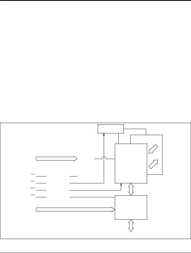
FUNCTIONAL DIAGRAM
A3–A6 |
|
|
ROW |
|
|
SELECT |
|
CE |
|
|
|
|
|
|
|
OE |
CONTROL |
|
|
|
|
||
|
|
||
WE |
LOGIC |
|
|
|
|
|
|
NE |
|
|
|
A0–A2 |
|
|
|
|
|
|
|
A7–A8 |
|
|
|
Write Enable (WE)
The Write Enable input controls the writing of data to both the static RAM and stores to the E2PROM.
Nonvolatile Enable (NE)
The Nonvolatile Enable input controls all accesses to the E2PROM array (store and recall functions).
PIN NAMES
Symbol |
Description |
|
|
A0–A8 |
Address Inputs |
I/O0–I/O7 |
Data Input/Output |
WE |
Write Enable |
|
|
CE |
Chip Enable |
OE |
Output Enable |
|
|
NE |
Nonvolatile Enable |
|
|
VCC |
+5V |
VSS |
Ground |
NC |
No Connect |
|
|
3825 PGM T01
VCC SENSE
EEPROM ARRAY
512 x 8 |
RECALL |
SRAM |
|
ARRAY |
STORE |
|
COLUMN SELECT
&
I/OS
I/O0–I/O7 |
3825 FHD F01 |
|
2

X20C04
DEVICE OPERATION
The CE, OE, WE and NE inputs control the X20C04 operation. The X20C04 byte-wide NOVRAM uses a 2-line control architecture to eliminate bus contention in a system environment. The I/O bus will be in a high impedance state when either OE or CE is HIGH, or when NE is LOW.
RAM Operations
RAM read and write operations are performed as they would be with any static RAM. A read operation requires CE and OE to be LOW with WE and NE HIGH. A write operation requires CE and WE to be LOW with NE HIGH. There is no limit to the number of read or write operations performed to the RAM portion of the X20C04.
Nonvolatile Operations
With NE LOW, recall operation is performed in the same manner as RAM read operation. A recall operation causes the entire contents of the E2PROM to be written into the RAM array. The time required for the operation to complete is 5μs or less. A store operation causes the entire contents of the RAM array to be stored in the nonvolatile E2PROM. The time for the operation to complete is 5ms or less.
Power-Up Recall
Upon power-up (VCC), the X20C04 performs an automatic array recall. When VCC minimum is reached, the
recall is initiated, regardless of the state of CE, OE, WE and NE.
Write Protection
The X20C04 has five write protect features that are employed to protect the contents of both the nonvolatile memory and the RAM.
•VCC Sense—All functions are inhibited when VCC is ≤ 3.5V.
•A RAM write is required before a Store Cycle is initiated.
•Write Inhibit—Holding either OE LOW, WE HIGH, CE HIGH, or NE HIGH during power-up and powerdown will prevent an inadvertent store operation.
•Noise Protection—A combined WE, NE, OE and CE pulse of less than 20ns will not initiate a Store Cycle.
•Noise Protection—A combined WE, NE, OE and CE pulse of less than 20ns will not initiate a recall cycle.
SYMBOL TABLE
WAVEFORM INPUTS |
OUTPUTS |
||||||||
|
|
|
|
|
|
|
|
Must be |
Will be |
|
|
|
|
|
|
|
|
||
|
|
|
|
|
|
|
|
steady |
steady |
|
|
|
|
|
|
|
|
May change |
Will change |
|
|
|
|
|
|
|
|
||
|
|
|
|
|
|
|
|
from LOW |
from LOW |
|
|
|
|
|
|
|
|
to HIGH |
to HIGH |
|
|
|
|
|
|
|
|
||
|
|
|
|
|
|
|
|
May change |
Will change |
|
|
|
|
|
|
|
|
||
|
|
|
|
|
|
|
|
from HIGH |
from HIGH |
|
|
|
|
|
|
|
|
to LOW |
to LOW |
|
|
|
|
|
|
|
|
||
|
|
|
|
|
|
|
|
Don’t Care: |
Changing: |
|
|
|
|
|
|
|
|
||
|
|
|
|
|
|
|
|
Changes |
State Not |
|
|
|
|
|
|
|
|
Allowed |
Known |
|
|
|
|
|
|
|
|
||
|
|
|
|
|
|
|
|
N/A |
Center Line |
|
|
|
|
|
|
|
|
||
|
|
|
|
|
|
|
|
|
is High |
|
|
|
|
|
|
|
|
|
|
|
|
|
|
|
|
|
|
|
Impedance |
|
|
|
|
|
|
|
|
|
|
|
|
|
|
|
|
|
|
|
|
3

X20C04
ABSOLUTE MAXIMUM RATINGS* |
–65°C to +135°C |
Temperature under Bias .................. |
|
Storage Temperature ....................... |
–65°C to +150°C |
Voltage on any Pin with |
|
Respect to VSS ....................................... |
–1V to +7V |
D.C. Output Current ........................................... |
10mA |
Lead Temperature (Soldering, 10 seconds) ..... 300°C
RECOMMENDED OPERATING CONDITIONS
Temperature |
Min. |
Max. |
|
|
|
Commercial |
0°C |
+70°C |
|
|
|
Industrial |
–40°C |
+85°C |
|
|
|
Military |
–55°C |
+125°C |
|
|
|
3825 PGM T02.1
*COMMENT
Stresses above those listed under “Absolute Maximum Ratings” may cause permanent damage to the device. This is a stress rating only and the functional operation of the device at these or any other conditions above those indicated in the operational sections of this specification is not implied. Exposure to absolute maximum rating conditions for extended periods may affect device reliability.
Supply Voltage |
Limits |
|
|
X20C04 |
5V ±10% |
|
|
3825 PGM T03
D.C. OPERATING CHARACTERISTICS (Over recommended operating conditions unless otherwise specified.)
|
|
|
Limits |
|
|
|
|
|
|
|
|
Symbol |
Parameter |
Min. |
Max. |
Units |
Test Conditions |
|
|
|
|
|
|
lCC1 |
VCC Current (Active) |
|
100 |
mA |
NE = WE = VIH, CE = OE = VIL |
|
|
|
|
|
Address Inputs = 0.4V/2.4V levels |
|
|
|
|
|
@ f = 5MHz. All I/Os = Open |
|
|
|
|
|
|
ICC2 |
VCC Current During Store |
|
10 |
mA |
All Inputs = VIH |
|
|
|
|
|
All I/Os = Open |
ISB1 |
VCC Standby Current |
|
10 |
mA |
CE = VIH |
|
(TTL Input) |
|
|
|
All Other Inputs = VIH, All I/Os = Open |
ISB2 |
VCC Standby Current |
|
250 |
μA |
All Inputs = VCC – 0.3V |
|
(CMOS Input) |
|
|
|
All I/Os = Open |
ILI |
Input Leakage Current |
|
10 |
μA |
VIN = VSS to VCC |
ILO |
Output Leakage Current |
|
10 |
μA |
VOUT = VSS to VCC, CE = VIH |
VIL(1) |
Input LOW Voltage |
–1 |
0.8 |
V |
|
V (1) |
Input HIGH Voltage |
2 |
V + 0.5 |
V |
|
IH |
|
|
CC |
|
|
VOL |
Output LOW Voltage |
|
0.4 |
V |
IOL = 2.1mA |
VOH |
Output HIGH Voltage |
2.4 |
|
V |
IOH = –400μA |
|
|
|
|
|
|
|
|
|
3825 PGM T04.3 |
POWER-UP TIMING |
|
|
|
|
|
|
|
||
|
|
|
|
|
|
|
|
|
|
Symbol |
|
Parameter |
|
|
Max. |
Units |
|||
|
|
|
|
|
|
|
|
|
|
tPUR(2) |
|
Power-Up to RAM Operation |
|
|
100 |
|
μs |
||
tPUW(2) |
|
Power-Up to Nonvolatile Operation |
|
|
5 |
|
ms |
||
|
|
|
|
|
|
|
|
|
3825 PGM T05 |
CAPACITANCE TA = +25°C, F = 1MHz, VCC = 5V. |
|
|
|
|
|
||||
|
|
|
|
|
|
|
|
|
|
Symbol |
|
Test |
|
Max. |
|
Units |
|
Conditions |
|
|
|
|
|
|
|
|
|
|
|
CI/O(2) |
|
Input/Output Capacitance |
|
10 |
|
pF |
|
VI/O = 0V |
|
C (2) |
|
Input Capacitance |
|
6 |
|
pF |
|
V = 0V |
|
IN |
|
|
|
|
|
|
|
IN |
|
3825 PGM T06.1
Notes: (1) VIL min. and VIH max. are for reference only and are not tested.
(2) This parameter is periodically sampled and not 100% tested.
4
X20C04
ENDURANCE AND DATA RETENTION
|
Parameter |
|
|
|
|
Min. |
|
|
|
Units |
|||
|
|
|
|
|
|
|
|
|
|
|
|
|
|
|
Endurance |
|
|
|
100,000 |
|
Data Changes Per Bit |
||||||
|
Store Cycles |
|
|
|
1,000,000 |
|
|
|
Store Cycles |
||||
|
|
|
|
|
|
|
|
|
|
|
|
|
|
|
Data Retention |
100 |
|
|
|
|
Years |
||||||
|
|
|
|
|
|
|
|
|
|
|
|
|
|
|
|
|
|
|
|
|
|
|
|
|
|
|
3825 PGM T07.1 |
MODE SELECTION |
|
|
|
|
|
|
|
|
|
|
|
||
|
|
|
|
|
|
|
|
|
|
|
|||
CE |
WE |
NE |
|
OE |
|
Mode |
|
I/O |
|
Power |
|||
|
|
|
|
|
|
|
|
|
|
||||
H |
X |
X |
|
X |
|
Not Selected |
Output High Z |
|
Standby |
||||
|
|
|
|
|
|
|
|
|
|
||||
L |
H |
H |
|
L |
|
Read RAM |
Output Data |
|
Active |
||||
L |
L |
H |
|
H |
|
Write “1” RAM |
Input Data High |
|
Active |
||||
|
|
|
|
|
|
|
|
|
|
||||
L |
L |
H |
|
H |
|
Write “0” RAM |
Input Data Low |
|
Active |
||||
|
|
|
|
|
|
|
|
|
|
||||
L |
H |
L |
|
L |
|
Array Recall |
Output High Z |
|
Active |
||||
L |
L |
L |
|
H |
|
Nonvolatile Storing |
Output High Z |
|
Active |
||||
|
|
|
|
|
|
|
|
|
|
||||
L |
H |
H |
|
H |
|
Output Disabled |
Output High Z |
|
Active |
||||
|
|
|
|
|
|
|
|
|
|
||||
L |
L |
L |
|
L |
|
Not Allowed |
Output High Z |
|
Active |
||||
L |
H |
L |
|
H |
|
No Operation |
Output High Z |
|
Active |
||||
|
|
|
|
|
|
|
|
|
|
|
|
|
3825 PGM T09.1 |
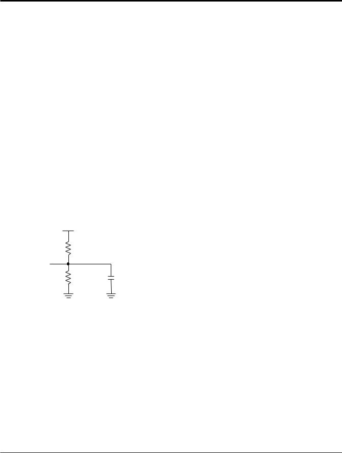
EQUIVALENT A.C. LOAD CIRCUIT |
|
|
A.C. CONDITIONS OF TEST |
|
|
||||||||
|
|
|
|
|
|
|
|
|
|
|
|
|
|
|
|
5V |
|
|
|
|
|
|
Input Pulse Levels |
|
|
0V to 3V |
|
|
|
|
|
|
|
|
|
Input Rise and |
|
|
|
||
|
|
|
|
|
|
|
|
|
|
|
|
||
|
|
|
1.92KΩ |
|
|
|
Fall Times |
|
|
10ns |
|||
|
|
|
|
|
|
|
|
|
|
|
|||
|
|
|
|
|
|
Input and Output |
|
|
|
||||
|
|
|
|
|
|
|
|
|
|
|
|
||
|
|
|
|
|
|
|
|
|
Timing Levels |
|
|
1.5V |
|
|
OUTPUT |
|
|
|
|
|
|
|
|
|
|
|
|
|
|
|
|
|
|
|
|
|
|
|
|
3825 PGM T08.2 |
|
|
|
|
1.37KΩ |
100pF |
|
|
|
|
|
|
|
||
|
|
|
|
|
|
3825 FHD F04.1 |
|
|
|
|
|
|
|
|
|
|
|
|
|
|
|
|
|
|
|
|
|
5
 Loading...