White Electronic Designs EDI9F416128LP85BNC, EDI9F416128LP70BNC, EDI9F416128LP100BNC, EDI9F416128C85BNC, EDI9F416128C100BNC Datasheet

EDI9F416128C
4x128Kx16 Static RAM CMOS, Module
FEATURES
ν4x128Kx16 bit CMOS Static
νRandom Access Memory
•Access Times 70 thru 100ns
•Data Retention Function (EDI9F416128LP )
•TTL Compatible Inputs and Outputs
•Fully Static, No Clocks
νHigh Density Packaging
•80 Pin SIMM, No. 318
νSingle +5V (±10%) Supply Operation
DESCRIPTION
The EDI9F416128C is a 8192K bit CMOS Static RAM based on eight 128Kx8 Static RAMs mounted on a multi-layered epoxy laminate (FR-4) substrate.
A low power version with data retention (EDI9F416128LP) is also available.
All inputs and outputs are TTL compatible and operate from a single +5V supply. Fully asynchronous, the EDI9F416128C requires no clocks or refreshing for operation.
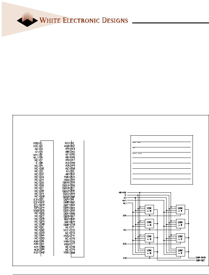
FIG. 1
PIN CONFIGURATIONS AND BLOCK DIAGRAM |
PIN NAMES |
AØ-A16 |
Address Inputs |
EØ-E3 |
Chip Enable |
G |
Output Enables |
WH-WL |
Write Enables |
E |
Chip Select |
DQØ-DQ15 |
Data Input/Output |
VCC |
Supply 5 Volts |
VSS |
Ground |
NC |
No Connect |
Aug. 2002 Rev. 2A |
1 |
White Electronic Designs Corporation • (508) 366-5151 • www.whiteedc.com |
ECO #15521 |
|
|

EDI9F416128C
ABSOLUTE MAXIMUM RATINGS*
Voltage on any pin relative to VSS |
-0.5V to 7.0V |
Operating Temperature TA (Ambient) |
|
Commercial |
0°C to +70°C |
Industrial |
-40°C to +85°C |
Storage Temperature |
|
Plastic |
-55°C to +125°C |
Power Dissipation |
1 Watt |
Output Current. |
20 mA |
*Stress greater than those listed under "Absolute Maximum Ratings" may cause permanent damage to the device. This is a stress rating only and functional operation of the device at these or any other conditions greater than those indicated in the operational sections of this specification is not implied. Exposure to absolute maximum rating conditions for extended periods may affect reliability.
RECOMMENDED DC OPERATING CONDITIONS
Parameter |
Sym |
Min |
Typ |
Max |
Units |
|
Supply Voltage |
VCC |
4.5 |
5.0 |
5.5 |
V |
|
Supply Voltage |
VSS |
0 |
0 |
0 |
V |
|
Input High Voltage |
VIH |
2.2 |
-- |
6.0 |
V |
|
Input Low Voltage |
VIL |
-0.3 |
-- |
0.8 |
V |
|
AC TEST CONDITIONS
Input Pulse Levels |
VSS to 3.0V |
||
Input Rise and Fall Times |
5ns |
|
|
Input and Output Timing Levels |
1.5V |
|
|
Output Load 70ns |
1TTL = 30pF |
|
|
85-120ns |
1TTL, CL =100pF |
|
|
(note: For TEHQZ,TGHQZ and TWLQZ, CL = 5pF)
DC ELECTRICAL CHARACTERISTICS
Parameter |
Sym |
|
|
|
|
|
|
Conditions |
|
Min |
Typ |
Max |
Units |
||
Operating Power |
ICC1 |
W, |
|
E |
= VIL, II/O = 0mA, |
|
-- |
94 |
158 |
mA |
|
||||
Supply Current |
|
|
|
|
|
|
|
|
Min Cycle |
|
|
|
|
|
|
Standby (TTL) Power |
ICC2 |
|
E |
³ VIH, VIN £ VIL |
|
-- |
56 |
120 |
mA |
|
|||||
Supply Current |
|
|
|
|
|
|
|
|
VIN ³ VIH |
|
|
|
|
|
|
Full Standby Power |
ICC3 |
|
|
|
|
|
E |
³ VCC-0.2V |
C |
-- |
|
24 |
mA |
|
|
Supply Current |
|
VIN ³ VCC-0.2V or |
LP |
-- |
|
80 |
µA |
||||||||
CMOS |
|
|
|
|
|
|
|
|
VIN £ 0.2V |
|
|
|
|
|
|
Input Leakage Current |
ILI |
|
|
VIN = 0V to VCC |
|
-- |
-- |
±10 |
µA |
|
|||||
Output Leakage Current |
ILO |
|
|
V I/O = 0V to VCC |
|
-- |
-- |
±10 |
µA |
|
|||||
Output High Voltage |
VOH |
|
|
|
|
|
|
IOH = -1.0mA |
|
2.4 |
-- |
-- |
V |
|
|
Output Low Voltage |
VOL |
|
|
|
|
|
|
IOL = 2.1mA |
|
-- |
-- |
0.4 |
V |
|
|
TRUTH TABLE
|
|
|
|
|
|
|
|
|
|
|
|
|
G |
E |
W |
Mode |
Output |
Power |
|
||||
|
X |
H |
|
X |
Standby |
High Z |
ICC2, ICC3 |
|
|||
|
H |
L |
|
H |
Output Deselect |
High Z |
ICC1 |
|
|||
|
L |
L |
|
H |
Read |
DOUT |
ICC1 |
|
|||
|
X |
L |
|
L |
Write |
DIN |
ICC1 |
|
|||
CAPACITANCE
(f=1.0MHz, VIN=VCC or VSS)
Parameter |
Sym |
Max |
Unit |
Address Lines |
CI |
60 |
pF |
Data Lines |
CD/Q |
80 |
pF |
Chip Enable Line |
CC |
15 |
pF |
Write and Output Enable Lines |
CW |
60 |
pF |
White Electronic Designs Corporation • (508) 366-5151 • www.whiteedc.com |
2 |
Aug. 2002 Rev. 2A |
|
|
ECO #15521 |
 Loading...