


 Loading...
Western Digital HUS726T6TALE6L4, HUS726T6TALN6L4, HUS726T4TALE6L4, HUS726T4TALN6L4, HUS726T4TALA6L4 Manual
Hard Disk Drive Specifications
Ultrastar™ DC HC310
3.5 inch Serial ATA Hard Disk Drive
Models: HUS726T6TALE6L4 HUS726T6TALN6L4 HUS726T4TALE6L4 HUS726T4TALN6L4 HUS726T4TALA6L4
Revision 1.4
18 September 2018
Publication Disclaimer Information
One MB is equal to one million bytes, one GB is equal to one billion bytes and one TB equals 1,000GB (one trillion bytes) when referring to storage capacity. Accessible capacity will vary from the stated capacity due to formatting and partitioning of the drive, the computer’s operating system, and other factors.
The following paragraph does not apply to any jurisdiction where such provisions are inconsistent with local law: THIS PUBLICATION IS PROVIDED "AS IS" WITHOUT WARRANTY OF ANY KIND, EITHER EXPRESS OR IMPLIED, INCLUDING, BUT NOT LIMITED TO, THE IMPLIED WARRANTIES OF MERCHANTABILITY OR FITNESS FOR A PARTICULAR PURPOSE.
This publication could include technical inaccuracies or typographical errors. Changes are periodically made to the information herein; these changes will be incorporated in new editions of the publication. There may be improvements or changes in any products or programs described in this publication at any time. It is possible that this publication may contain reference to, or information about, Western Digital products (machines and programs), programming, or services that are not announced in your country. Such references or information must not be construed to mean t hat Western Digital Corporation intends to announce such Western Digital products, programming, or services in your country. Technical information about this product is available by contacting your local Western Digital product representative or on the Internet at: support@wdc.com.
Western Digital Corporation may have patents or pending patent applications covering subject matter in this document. The furnishing of this document does not give you any license to these patents.
© 2017 Western Digital Corporation or its affiliates.
Western Digital and Ultrastar are registered trademarks or trademarks of Western Digital Corporation or its affiliates in the U.S. and/or other countries. All other marks are the property of their respective owners.
References in this publication to Western Digital-branded products, programs, or services do not imply that they will be made available in all countries. Product specifications provided are sample specifications and do not constitute a warranty. Actual specifications for unique part numbers may vary. Please visit the Support section of our website, support@wdc.com, for additional information on product specifications. Pictures shown may vary from actual products.

Table of Contents
1 |
General |
........................................................................................................................................... |
1 |
|
|
1.1 |
Introduction.......................................................................................................................... |
1 |
|
|
1.2 |
Glossary ............................................................................................................................... |
2 |
|
|
1.3 |
General ...................................................................................................................Caution |
2 |
|
|
1.4 |
References ............................................................................................................................ |
2 |
|
2 |
General ..............................................................................................................................Features |
3 |
||
Part 1. Functional .............................................................................................................Specification |
4 |
|||
3 |
Fixed Disk .......................................................................................................Subsystem Description |
5 |
||
|
3.1 |
Control ...............................................................................................................Electronics |
5 |
|
|
3.2 |
Head .............................................................................................................Disk Assembly |
5 |
|
|
3.3 |
Actuator ............................................................................................................................... |
5 |
|
4 |
Drive Characteristics.......................................................................................................................... |
6 |
||
|
4.1 |
Default .........................................................................................Logical Drive Parameters |
6 |
|
|
4.2 |
Data ............................................................................................................................Sheet |
7 |
|
|
4.3 |
World ..............................................................................................Wide Name Assignment |
7 |
|
|
4.4 |
Drive ...............................................................................................................Organization |
8 |
|
|
4.4.1 ................................................................................................................. |
Drive Format |
8 |
|
|
4.4.2 ......................................................................................................... |
Cylinder Allocation |
8 |
|
|
4.5 |
Performance .................................................................................................Characteristics |
9 |
|
|
4.5.1 ................................................................................................... |
Mechanical Positioning |
9 |
|
|
4.5.2 .......................................................................................................... |
Drive Ready Time |
10 |
|
|
4.5.3 ........................................................................................................... |
Operating Modes |
10 |
|
5 |
Defect Flagging ...................................................................................................................Strategy |
12 |
||
|
5.1 |
Shipped ...................................................................................................................Format |
12 |
|
6 |
Specification.................................................................................................................................... |
13 |
||
|
6.1 |
Electrical ..............................................................................................................Interface |
13 |
|
|
6.1.1 ........................................................................................................ |
Connector Location |
13 |
|
|
6.1.2 ............................................................................................... |
Signal Definition (SATA) |
15 |
|
|
6.1.3 ....................................................................................... |
Out of Band Signaling (SATA) |
16 |
|
|
6.1.4 ........................................................................................... |
Voltage and Ground Signals |
16 |
|
|
6.1.5 ........................................................................................................ |
Ready LED Output |
16 |
|
|
6.2 |
Environment........................................................................................................................ |
17 |
|
|
6.2.1 ........................................................................................... |
Temperature and Humidity |
17 |
|
|
6.2.2 ................................................................................................... |
Storage Requirements |
18 |
|
|
6.2.3 ............................................................................................................... |
Corrosion Test |
18 |
|
|
6.2.4 .................................................................................................. |
Atmospheric Condition |
18 |
|
|
6.3 |
DC ......................................................................................................Power Requirements |
19 |
|
|
6.3.1 ................................................................................................................ |
Input Voltage |
19 |
|
|
6.3.2 ................................................................................................... |
Power Supply Current |
21 |
|
|
6.3.3 ................................................................................................ |
Power Line Noise Limits |
24 |
|
|
6.3.4 ....................................................................................... |
Power Consumption Efficiency |
24 |
|
|
6.4 |
Reliability ............................................................................................................................ |
25 |
|
|
6.4.1 ............................................................................................................... |
Data Integrity |
25 |
|
|
6.4.2 ............................................................................................... |
Cable Noise Interference |
25 |
|
|
6.4.3 .................................................................................................................. |
Load/Unload |
25 |
|
|
6.4.4 ........................................................................................................... |
Start/Stop Cycles |
25 |
|
|
6.4.5 ................................................................................................ |
Preventive Maintenance |
25 |
|
|
6.4.6 ............................................................................................................. |
Data Reliability |
25 |
|
|
6.5 |
Mechanical ....................................................................................................Specifications |
26 |
|
|
6.5.1 ...................................................................................................... |
Physical Dimensions |
26 |
|
|
6.5.2 ............................................................................................................. |
Drive Mounting |
27 |
|
|
6.5.3 |
Heads Unload and Actuator Lock ................................................................................... |
27 |
|
|
6.6 |
Vibration and Shock ............................................................................................................. |
28 |
|
|
6.6.1 |
Operating Vibration ...................................................................................................... |
28 |
|
|
6.6.2 |
Nonoperating Vibration ................................................................................................. |
29 |
|
|
6.6.3 |
Operating Shock ............................................................................................................ |
29 |
|
|
6.6.4 |
Nonoperating Shock ...................................................................................................... |
29 |
|
|
6.6.5 |
Nonoperating Rotational Shock ..................................................................................... |
30 |
|
|
6.7 |
Acoustics ............................................................................................................................. |
31 |
|
|
6.8 |
Identification Labels ............................................................................................................ |
31 |
|
|
6.9 |
Safety .................................................................................................................................. |
32 |
|
|
6.9.1 |
UL and CSA Standard Conformity ................................................................................. |
32 |
|
|
6.9.2 |
European Safety Mark .................................................................................................. |
32 |
|
|
6.9.3 |
Flammability ................................................................................................................ |
32 |
|
|
6.9.4 |
Safe Handling ............................................................................................................... |
32 |
|
|
6.9.5 |
Substance Restriction Requirements .............................................................................. |
32 |
|
|
6.9.6 |
Secondary Circuit Protection ......................................................................................... |
32 |
|
|
6.10 |
|
Electromagnetic Compatibility .......................................................................................... |
33 |
|
6.10.1 |
CE Mark ....................................................................................................................... |
33 |
|
|
6.10.2 |
RCM Mark .................................................................................................................... |
33 |
|
|
6.10.3 |
BSMI Mark ................................................................................................................... |
33 |
|
|
6.10.4 |
KC Mark ....................................................................................................................... |
34 |
|
|
6.11 |
|
Third Party Notices .......................................................................................................... |
34 |
Part 2. Interface Specification............................................................................................................... |
35 |
|||
7 |
General .......................................................................................................................................... |
|
36 |
|
|
7.1 |
Introduction......................................................................................................................... |
36 |
|
|
7.2 |
Terminology ......................................................................................................................... |
36 |
|
|
7.3 |
Deviations From Standard ................................................................................................... |
36 |
|
8 |
Registers ........................................................................................................................................ |
37 |
||
|
8.1 |
Alternate Status Register ..................................................................................................... |
37 |
|
|
8.2 |
Command Register .............................................................................................................. |
37 |
|
|
8.3 |
Cylinder High Register ........................................................................................................ |
37 |
|
|
8.4 |
Cylinder Low Register.......................................................................................................... |
38 |
|
|
8.5 |
Device Control Register ........................................................................................................ |
38 |
|
|
8.6 |
Device/Head Register ........................................................................................................... |
38 |
|
|
8.7 |
Error Register ...................................................................................................................... |
39 |
|
|
8.8 |
Features Register ................................................................................................................ |
39 |
|
|
8.9 |
Sector Count Register .......................................................................................................... |
39 |
|
|
8.10 |
|
Sector Number Register .................................................................................................... |
39 |
|
8.11 |
|
Status Register ................................................................................................................. |
40 |
9 |
General Operation Descriptions.......................................................................................................... |
41 |
||
|
9.1 |
Reset Response .................................................................................................................... |
41 |
|
|
9.1.1 |
Register Initialization.................................................................................................... |
42 |
|
|
9.2 |
Diagnostic and Reset Considerations .................................................................................... |
42 |
|
|
9.3 |
Sector Addressing Mode ....................................................................................................... |
43 |
|
|
9.3.1 |
Logical CHS Addressing Mode ....................................................................................... |
43 |
|
|
9.3.2 |
LBA Addressing Mode ................................................................................................... |
43 |
|
|
9.4 |
Power Management Feature ................................................................................................ |
44 |
|
|
9.4.1 |
Power Mode .................................................................................................................. |
44 |
|
|
9.4.2 |
Power Management Commands ..................................................................................... |
45 |
|
|
9.4.3 |
Standby Timer .............................................................................................................. |
45 |
|
|
9.4.4 |
Interface Capability for Power Modes ............................................................................ |
45 |
|
|
9.5 |
SMART Function ................................................................................................................. |
46 |
|
|
9.5.1 |
Attributes ..................................................................................................................... |
46 |
|
|
9.5.2 |
Attribute Values ............................................................................................................ |
46 |
|
9.5.3 |
Attribute Thresholds ..................................................................................................... |
46 |
|
9.5.4 |
Threshold Exceeded Condition ....................................................................................... |
46 |
|
9.5.5 |
SMART Commands ....................................................................................................... |
46 |
|
9.5.6 |
Off-Line Read Scanning................................................................................................. |
46 |
|
9.5.7 |
Error Log ...................................................................................................................... |
47 |
|
9.5.8 |
Self-Test ........................................................................................................................ |
47 |
|
9.6 |
Security Mode Feature Set ................................................................................................... |
48 |
|
9.6.1 |
Security Mode ............................................................................................................... |
48 |
|
9.6.2 |
Security Level ............................................................................................................... |
48 |
|
9.6.3 |
Password....................................................................................................................... |
48 |
|
9.6.4 |
Operation Example ....................................................................................................... |
49 |
|
9.6.5 |
Command Table ............................................................................................................ |
52 |
|
9.7 |
Host Protected Area Feature ................................................................................................ |
55 |
|
9.7.1 |
Example for Operation (in LBA mode)............................................................................ |
55 |
|
9.7.2 |
Security Extensions....................................................................................................... |
56 |
|
9.8 |
Write Cache Function .......................................................................................................... |
57 |
|
9.9 |
Reassign Function ............................................................................................................... |
57 |
|
9.9.1 |
Auto Reassign Function ................................................................................................. |
57 |
|
9.10 |
|
Power-Up in Standby Feature Set ..................................................................................... |
58 |
9.11 |
|
Advanced Power Management Feature Set (APM)............................................................. |
58 |
9.12 |
|
48-bit Address Feature Set................................................................................................ |
58 |
9.13 |
|
Streaming Feature Set...................................................................................................... |
59 |
9.13.1 |
Streaming Commands ................................................................................................... |
59 |
|
9.14 |
|
SATA BIST (built-in self-test)............................................................................................ |
61 |
9.15 |
|
SATA Interface Power Management .................................................................................. |
62 |
9.15.1 |
Low PHY Power Conditions Overview ............................................................................ |
62 |
|
9.15.2 |
Active PHY Power Condition ......................................................................................... |
62 |
|
9.15.3 |
Partial PHY Power Condition ........................................................................................ |
62 |
|
9.15.4 |
Slumber PHY Power Condition ...................................................................................... |
62 |
|
9.16 |
|
Software Setting Preservation .......................................................................................... |
63 |
9.16.1 |
COMRESET Preservation Requirements ....................................................................... |
63 |
|
9.17 |
|
Serial ATA Optional Features ............................................................................................ |
64 |
9.17.1 |
Asynchronous Signal Recovery ...................................................................................... |
64 |
|
9.17.2 |
Device Power Connector Pin 11 Definition ...................................................................... |
64 |
|
9.17.3 |
Phy Event Counters ...................................................................................................... |
64 |
|
9.17.4 |
NCQ NON-DATA (63h) .................................................................................................. |
69 |
|
9.17.5 |
Rebuild Assist ............................................................................................................... |
73 |
|
9.17.6 |
Power Disable ............................................................................................................... |
74 |
|
9.18 |
|
SCT Command Transport Feature Set .............................................................................. |
75 |
9.18.1 |
Overview....................................................................................................................... |
75 |
|
9.18.2 |
SCT Command Protocol ................................................................................................. |
77 |
|
9.18.3 |
SCT Command Set ........................................................................................................ |
85 |
|
9.19 |
|
Extended Power Conditions (EPC) Feature ....................................................................... |
93 |
9.19.1 |
Power Conditions .......................................................................................................... |
93 |
|
9.19.2 |
Power Condition Timers ................................................................................................ |
94 |
|
9.19.3 |
Interaction with Resets, Commands and other Features ................................................. |
94 |
|
9.20 |
|
Sanitize Device Feature Set .............................................................................................. |
95 |
9.20.1 |
Overview....................................................................................................................... |
95 |
|
9.20.2 |
Sanitize Device Feature................................................................................................. |
96 |
|
9.20.3 |
Sanitize Device State Machine....................................................................................... |
97 |
|
9.21 |
|
Trusted Computing Group Feature Set .............................................................................. |
99 |
9.21.1 |
Referenced Specifications and Standards ....................................................................... |
99 |
|
9.21.2 |
Implementation Exceptions ......................................................................................... |
100 |
|
9.21.3 |
Implementation Features and Details Outside of TCG Specifications ........................... |
100 |
|
|
9.21.4 |
|
Encryption Algorithms ................................................................................................ |
101 |
|
9.21.5 |
|
TCG Enterprise SSC Tables......................................................................................... |
102 |
|
9.21.6 Firmware Download and Signing ................................................................................. |
105 |
||
|
9.21.7 |
|
Ports ........................................................................................................................... |
105 |
|
9.21.8 |
|
MSID .......................................................................................................................... |
108 |
|
9.21.9 |
|
Logging ....................................................................................................................... |
108 |
|
9.21.10 |
Number of Sessions .................................................................................................. |
108 |
|
|
9.21.11 |
Number of Bands ..................................................................................................... |
108 |
|
|
9.21.12 |
Number of COMIDs ................................................................................................. |
108 |
|
|
9.21.13 |
PSID........................................................................................................................ |
108 |
|
|
9.21.14 Locked and Unlocked Behavior ................................................................................. |
109 |
||
|
9.21.15 |
Error Codes.............................................................................................................. |
114 |
|
|
9.21.16 |
Life Cycle model....................................................................................................... |
114 |
|
|
9.21.17 |
Customer Specific Requirements .............................................................................. |
114 |
|
10 |
Command Protocol......................................................................................................................... |
115 |
||
|
10.1 |
PIO Data In commands................................................................................................... |
115 |
|
|
10.2 |
PIO Data Out commands ................................................................................................ |
115 |
|
|
10.3 |
Non-Data commands ...................................................................................................... |
116 |
|
|
10.4 |
DMA Data In commands and DMA Data Out commands ................................................. |
117 |
|
|
10.5 |
First-party DMA commands ............................................................................................ |
117 |
|
11 |
Command Descriptions................................................................................................................... |
118 |
||
|
11.1 |
Check Power Mode (E5h/98h).......................................................................................... |
123 |
|
|
11.2 |
Configure Stream (51h)................................................................................................... |
124 |
|
|
11.3 |
Device Configuration Overlay (B1h) ................................................................................ |
126 |
|
|
11.3.1 |
|
Device Configuration Restore (Subcommand C0h) ........................................................ |
127 |
|
11.3.2 |
|
Device Configuration Freeze Lock (Subcommand C1h) ................................................. |
127 |
|
11.3.3 |
|
Device Configuration Identify (Subcommand C2h) ....................................................... |
127 |
|
11.3.4 Device Configuration Set (Subcommand C3h) .............................................................. |
127 |
||
|
11.4 |
Download Microcode (92h) .............................................................................................. |
130 |
|
|
11.5 |
Download Microcode DMA (93h)...................................................................................... |
132 |
|
|
11.6 |
Execute Device Diagnostic (90h) ..................................................................................... |
134 |
|
|
11.7 |
Flush Cache (E7h) .......................................................................................................... |
135 |
|
|
11.8 |
Flush Cache Ext (EAh) ................................................................................................... |
136 |
|
|
11.9 |
Format Track (50h)......................................................................................................... |
137 |
|
|
11.10 |
Format Unit (F7h) .......................................................................................................... |
138 |
|
|
11.11 |
Identify Device (ECh)...................................................................................................... |
139 |
|
|
11.12 |
Idle (E3h/97h)................................................................................................................. |
150 |
|
|
11.13 |
Idle Immediate (E1h/95h) ............................................................................................... |
151 |
|
|
11.14 |
Initialize Device Parameters (91h) .................................................................................. |
152 |
|
|
11.15 |
NCQ NON-DATA (63h) ................................................................................................... |
153 |
|
|
11.15.1 Abort NCQ Queue Subcommand (0h)........................................................................ |
154 |
||
|
11.15.2 |
Deadline handling Subcommand (1h) ....................................................................... |
156 |
|
|
11.15.3 |
Set Features Subcommand (5h) ................................................................................ |
158 |
|
|
11.16 |
RECEIVE FPDMA QUEUED (65h) ................................................................................. |
160 |
|
|
11.16.1 READ LOG DMA EXT (1h)....................................................................................... |
161 |
||
|
11.17 |
SEND FPDMA QUEUED (64h)....................................................................................... |
163 |
|
|
11.17.1 |
WRITE LOG DMA EXT (2h)..................................................................................... |
164 |
|
|
11.18 |
Read Buffer (E4h) ........................................................................................................... |
166 |
|
|
11.19 |
Read Buffer DMA (E9h) .................................................................................................. |
167 |
|
|
11.20 |
Read DMA(C8h/C9h) ...................................................................................................... |
168 |
|
|
11.21 |
Read DMA Ext (25h) ....................................................................................................... |
170 |
|
|
11.22 |
Read FPDMA Queued (60h) ............................................................................................ |
172 |
|
|
11.23 |
Read Log Ext (2Fh)......................................................................................................... |
174 |
|
|
11.23.1 |
General Purpose Log Directory ................................................................................. |
176 |
|
11.23.2 |
Extended Comprehensive SMART Error log ............................................................. |
177 |
|
11.23.3 |
Device Statistics log ................................................................................................. |
180 |
|
11.23.4 |
Extended Self-test log sector ..................................................................................... |
186 |
|
11.23.5 |
Power Conditions log................................................................................................ |
187 |
|
11.23.6 |
Queued Error Log .................................................................................................... |
190 |
|
11.23.7 |
Read Stream Error log ............................................................................................. |
191 |
|
11.23.8 |
Write Stream Error log............................................................................................. |
192 |
|
11.23.9 |
Identify Device Data log ........................................................................................... |
193 |
|
11.24 |
Read Log DMA Ext(47h) ................................................................................................. |
205 |
|
11.25 |
Read Multiple (C4h) ....................................................................................................... |
206 |
|
11.26 |
Read Multiple Ext (29h).................................................................................................. |
207 |
|
11.27 |
Read Native Max Address (F8h) ...................................................................................... |
209 |
|
11.28 |
Read Native Max Address Ext (27h) ................................................................................ |
210 |
|
11.29 |
Read Sector(s) (20h/21h) ................................................................................................. |
211 |
|
11.30 |
Read Sector(s) Ext (24h) ................................................................................................. |
212 |
|
11.31 |
Read Stream DMA Ext(2Ah) ........................................................................................... |
213 |
|
11.32 |
Read Stream Ext (2Bh) ................................................................................................... |
216 |
|
11.33 |
Read Verify Sector(s) (40h/41h) ....................................................................................... |
219 |
|
11.34 |
Read Verify Sector(s) Ext (42h) ....................................................................................... |
220 |
|
11.35 |
Recalibrate (1xh) ............................................................................................................ |
221 |
|
11.36 |
Request Sense Data Ext (0Bh) ........................................................................................ |
222 |
|
11.37 |
Sanitize Device Feature Set (B4h) ................................................................................... |
224 |
|
11.37.1 |
Crypto Scramble Ext Command (feature: 0011h)....................................................... |
224 |
|
11.37.2 |
Overwrite Ext Command (feature: 0014h)................................................................. |
226 |
|
11.37.3 |
Sanitize Freeze Lock Ext Command (feature: 0020h) ................................................ |
228 |
|
11.37.4 |
Sanitize Status Ext Command (feature: 0000h)......................................................... |
230 |
|
11.38 |
Security Disable Password (F6h)..................................................................................... |
232 |
|
11.39 |
Security Erase Prepare (F3h) .......................................................................................... |
233 |
|
11.40 |
Security Erase Unit (F4h) ............................................................................................... |
234 |
|
11.41 |
Security Freeze Lock (F5h) ............................................................................................. |
236 |
|
11.42 |
Security Set Password (F1h) ........................................................................................... |
237 |
|
11.43 |
Security Unlock (F2h) ..................................................................................................... |
239 |
|
11.44 |
Seek (7xh) ...................................................................................................................... |
240 |
|
11.45 |
Sense Condition (F0h : Vendor specific) ........................................................................... |
241 |
|
11.46 |
Set Features (EFh) ......................................................................................................... |
242 |
|
11.46.1 |
Set Transfer Mode .................................................................................................... |
243 |
|
11.46.2 |
Write Cache ............................................................................................................. |
243 |
|
11.46.3 |
Serial ATA Feature ................................................................................................... |
243 |
|
11.46.4 |
Advanced Power Management .................................................................................. |
244 |
|
11.46.5 |
Set Maximum Host Interface Sector Time................................................................. |
244 |
|
11.46.6 |
Extended Power Conditions (EPC) feature ................................................................ |
245 |
|
11.47 Set Max Address (F9h).................................................................................................... |
252 |
||
11.47.1 |
Set Max Set Password (Feature = 01h) ..................................................................... |
254 |
|
11.47.2 |
Set Max Lock (Feature = 02h)................................................................................... |
255 |
|
11.47.3 |
Set Max Unlock (Feature = 03h) ............................................................................... |
256 |
|
11.47.4 |
Set Max Freeze Lock (Feature = 04h)........................................................................ |
257 |
|
11.48 |
Set Max Address Ext (37h).............................................................................................. |
258 |
|
11.49 |
Set Multiple (C6h) .......................................................................................................... |
260 |
|
11.50 |
Sleep (E6h/99h) .............................................................................................................. |
261 |
|
11.51 |
SMART Function Set (B0h)............................................................................................. |
262 |
|
11.51.1 |
SMART Subcommand .............................................................................................. |
263 |
|
11.51.2 |
Device Attributes Data Structure ............................................................................. |
267 |
|
11.51.3 |
Device Attribute Thresholds Data Structure ............................................................. |
272 |
|
11.51.4 |
SMART Log Directory .............................................................................................. |
273 |
|
11.51.5 |
SMART summary error log sector ............................................................................. |
273 |
|
11.51.6 |
Self-test log data structure ....................................................................................... |
275 |
|
11.51.7 |
Selective self-test log data structure ......................................................................... |
276 |
|
11.51.8 |
Error Reporting........................................................................................................ |
277 |
|
11.52 |
Standby (E2h/96h) .......................................................................................................... |
278 |
|
11.53 |
Standby Immediate (E0h/94h) ........................................................................................ |
279 |
|
11.54 |
Trusted Receive (5Ch) ..................................................................................................... |
280 |
|
11.55 |
Trusted Receive DMA (5Dh) ............................................................................................ |
281 |
|
11.56 |
Trusted Send (5Eh) ......................................................................................................... |
282 |
|
11.57 |
Trusted Send DMA (5Fh) ................................................................................................ |
283 |
|
11.58 |
Write Buffer (E8h) .......................................................................................................... |
284 |
|
11.59 |
Write Buffer DMA (EBh) ................................................................................................. |
285 |
|
11.60 |
Write DMA (CAh/CBh).................................................................................................... |
286 |
|
11.61 |
Write DMA FUA Ext (3Dh) ............................................................................................. |
287 |
|
11.62 |
Write DMA Ext (35h) ...................................................................................................... |
289 |
|
11.63 |
Write FPDMA Queued (61h) ........................................................................................... |
291 |
|
11.64 |
Write Log Ext (3Fh) ........................................................................................................ |
293 |
|
11.65 |
Write Log DMA Ext (57h)................................................................................................ |
294 |
|
11.66 |
Write Multiple (C5h)....................................................................................................... |
295 |
|
11.67 |
Write Multiple Ext (39h) ................................................................................................. |
296 |
|
11.68 |
Write Multiple FUA Ext (CEh) ........................................................................................ |
297 |
|
11.69 |
Write Sector(s) (30h/31h) ................................................................................................ |
299 |
|
11.70 |
Write Sector(s) Ext (34h)................................................................................................. |
300 |
|
11.71 |
Write Stream DMA Ext (3Ah) ......................................................................................... |
301 |
|
11.72 |
Write Stream Ext (3Bh) .................................................................................................. |
304 |
|
11.73 |
Write Uncorrectable Ext (45h)......................................................................................... |
307 |
|

List of Tables |
|
|
Table 1 |
R/N and Model#................................................................................................................ |
1 |
Table 2 |
Formatted Capacity .......................................................................................................... |
6 |
Table 3 |
Data Sheet ....................................................................................................................... |
7 |
Table 4 World Wide Name Assignment .......................................................................................... |
7 |
|
Table 5 |
Average Seek Time ........................................................................................................... |
9 |
Table 6 |
Single Track Seek Time .................................................................................................... |
9 |
Table 7 |
Latency Time.................................................................................................................... |
9 |
Table 8 |
Drive Ready Time............................................................................................................ |
10 |
Table 9 |
6TB Mode Transition Times ............................................................................................. |
11 |
Table 10 |
4TB Mode Transition Times ........................................................................................... |
11 |
Table 11 Interface Connector Pins and I/O Signals ....................................................................... |
15 |
|
Table 12 |
Parameter Descriptions ................................................................................................. |
16 |
Table 13 Temperature and Humidity ............................................................................................ |
17 |
|
Table 14 |
Input Voltage ................................................................................................................. |
19 |
Table 15 |
SATA Power Consumption, 6TB, 4k................................................................................ |
21 |
Table 16 |
SATA Power Consumption, 4TB, 4k................................................................................ |
22 |
Table 17 |
SATA Power Consumption, 4TB, 512n ............................................................................ |
23 |
Table 18 Allowable Power Supply Noise Limits at Drive Power Connector .................................... |
24 |
|
Table 19 |
Power Consumption Efficiency ....................................................................................... |
24 |
Table 20 |
Physical Dimensions ...................................................................................................... |
26 |
Table 21 Random Vibration PSD Profile Break Points (operating) ................................................. |
28 |
|
Table 22 Random Vibration (Rotational) PSD Profile Break Points ............................................... |
28 |
|
Table 23 Random Vibration PSD Profile Break Points (nonoperating) ........................................... |
29 |
|
Table 24 |
Sinusoidal Shock Wave .................................................................................................. |
30 |
Table 25 |
Rotational Shock............................................................................................................ |
30 |
Table 26 |
Sound Power Levels ....................................................................................................... |
31 |
Table 27 |
Alternate Status Register .............................................................................................. |
37 |
Table 28 |
Device Control Register ................................................................................................. |
38 |
Table 29 |
Device/Head Register ..................................................................................................... |
38 |
Table 30 |
Error Register ............................................................................................................... |
39 |
Table 31 |
Status Register .............................................................................................................. |
40 |
Table 32 |
Reset Response .............................................................................................................. |
41 |
Table 33 |
Default Register Values ................................................................................................. |
42 |
Table 34 |
Diagnostic Codes ........................................................................................................... |
42 |
Table 35 |
Power conditions ............................................................................................................ |
45 |
Table 36 Command table for device lock operation -1 .................................................................... |
52 |
|
Table 37 Command table for device lock operation -2 .................................................................... |
53 |
|
Table 38 Command table for device lock operation -3 .................................................................... |
54 |
|
Table 39 |
Phy Event Counter Identifiers ....................................................................................... |
65 |
Table 40 READ LOG EXT Log Page 11h data structure definition ................................................ |
68 |
|
Table 41 |
NCQ NON-DATA - Command definition ......................................................................... |
69 |
Table 42 |
Subcommand Field ........................................................................................................ |
69 |
Table 43 |
NCQ NON-DATA Log (12h) data structure definition ...................................................... |
71 |
Table 44 |
Rebuild Assist log (15h) data structure definition ........................................................... |
73 |
Table 45 |
SCT Log Page and Direction .......................................................................................... |
75 |
Table 46 Identify Device Information Word 206 ............................................................................ |
75 |
|
Table 47 Output Registers of SCT Command Using SMART ......................................................... |
77 |
|
Table 48 Input Registers of SCT Command Using SMART ........................................................... |
77 |
|
Table 49 Input Registers of SCT Command Using Write Log Ext .................................................. |
78 |
|
Table 50 Output Registers of SCT Command Using Write Log Ext ................................................ |
78 |
|
Table 51 |
Key Sector Format ......................................................................................................... |
79 |
Table 52 |
SCT Action Code List ..................................................................................................... |
79 |
Table 53 |
Extended Status Code.................................................................................................... |
80 |
Table 54 Input Registers of SCT Data Transfer Using SMART ..................................................... |
81 |
|
Table 55 Input Registers of SCT Data Transfer using Read/Write Log Ext .................................... |
81 |
|
Table 56 |
Input Registers of SCT Status Request Using SMART .................................................... |
82 |
Table 57 |
Input Registers of SCT Status Request Using Read Log Ext ........................................... |
82 |
Table 58 Data Format of SCT Status Response -1 ......................................................................... |
83 |
|
Table 59 Data Format of SCT Status Response -2 ......................................................................... |
84 |
|
Table 60 |
SCT Write Same (Inputs) ............................................................................................... |
85 |
Table 61 Output Registers of SCT Write Same (Success) ............................................................... |
85 |
|
Table 62 Output Registers of SCT Write Same (Error) .................................................................. |
86 |
|
Table 63 Error Recovery Control Command (Inputs)..................................................................... |
87 |
|
Table 64 Error Recovery Control Command (On puts) .................................................................. |
87 |
|
Table 65 Feature Control Command (Inputs)................................................................................ |
88 |
|
Table 66 Feature Control Command (Outputs) ............................................................................. |
88 |
|
Table 67 Feature Code List .......................................................................................................... |
89 |
|
Table 68 |
SCT Data Table Command (Inputs)................................................................................ |
90 |
Table 69 |
SCT Data Table Command (Outputs) ............................................................................. |
90 |
Table 70 |
Table ID ........................................................................................................................ |
90 |
Table 71 Data Format of HDA Absolute Temperature History Table -1 .......................................... |
91 |
|
Table 72 Data Format of HDA Absolute Temperature History Table -2 .......................................... |
92 |
|
Table 73 |
Extended Power Conditions Subcommands .................................................................... |
93 |
Table 74 |
Power Condition IDs ...................................................................................................... |
93 |
Table 75 Vendor Specific Data for Level 0 Discovery ................................................................... |
101 |
|
Table 76 |
WDC Default Values for ‘Admin SP’ C_PIN & ‘Locking SP’ C_PIN ................................ |
102 |
Table 77 WDC Implementation of K_AES_256 Table .................................................................. |
103 |
|
Table 78 WDC Implementation of ‘Locking SP’ Access Control Table ........................................... |
103 |
|
Table 79 |
WDC Implementation of ‘Locking Info’ Table ................................................................ |
104 |
Table 80 WDC Implementation of ‘Locking SP’ Locking Table ..................................................... |
104 |
|
Table 81 |
Ports Functionality ...................................................................................................... |
105 |
Table 82 |
Ports Table .................................................................................................................. |
105 |
Table 83 |
Modified ‘Admin SP’ ACE Table.................................................................................... |
106 |
Table 84 |
Modified ‘Admin SP’ Access Control Table (part 1 of 2) .................................................. |
106 |
Table 85 |
Modified ‘Admin SP’ Access Control Table (part 2 of 2) .................................................. |
107 |
Table 86 |
Command table for TCG Enterprise device lock operation -1......................................... |
109 |
Table 87 |
Command table for TCG Enterprise device lock operation -2......................................... |
110 |
Table 88 |
Command table for TCG Enterprise device lock operation -3......................................... |
111 |
Table 89 |
TCG Enterprise SSC Commands Behavior -1 ............................................................... |
112 |
Table 90 |
TCG Enterprise SSC Commands Behavior -2 ............................................................... |
112 |
Table 91 |
TCG Enterprise SSC Commands Behavior -3 ............................................................... |
112 |
Table 92 |
TCG Enterprise SSC Commands Behavior -4 ............................................................... |
113 |
Table 93 |
TCG Enterprise SSC Commands Behavior -5 ............................................................... |
113 |
Table 94 |
TCG Enterprise SSC Commands Behavior -6 ............................................................... |
113 |
Table 95 |
Command Set .............................................................................................................. |
118 |
Table 96 |
Command Set –Continued–.......................................................................................... |
119 |
Table 97 |
Command Set –Continued–.......................................................................................... |
120 |
Table 98 |
Command Set (Subcommand) ...................................................................................... |
121 |
Table 99 Check Power Mode Command (E5h/98h) ...................................................................... |
123 |
|
Table 100 |
Configure Stream Command (51h) ............................................................................. |
124 |
Table 101 Device Configuration Overlay Command (B1h) ........................................................... |
126 |
|
Table 102 Device Configuration Overlay Features register values ............................................... |
126 |
|
Table 103 Device Configuration Overlay Data structure ............................................................. |
128 |
|
Table 104 |
DCO error information definition ............................................................................... |
129 |
Table 105 Download Microcode Command (92h) ......................................................................... |
130 |
|
Table 106 Download Microcode DMA Command (93h) ................................................................ |
132 |
|
Table 107 |
Execute Device Diagnostic Command (90h) ................................................................ |
134 |
Table 108 Flush Cache Command (E7h) ..................................................................................... |
135 |
|
Table 109 Flush Cache Ext Command (EAh) .............................................................................. |
136 |
|
Table 110 |
Format Track Command (50h).................................................................................... |
137 |
Table 111 Format Unit Command (F7h) ..................................................................................... |
138 |
|
Table 112 |
Identify Device Command (ECh) ................................................................................ |
139 |
Table 113 |
Identify device information ......................................................................................... |
140 |
Table 114 |
Identify device information -Continued-...................................................................... |
141 |
Table 115 |
Identify device information -Continued-...................................................................... |
142 |
Table 116 |
Identify device information -Continued-...................................................................... |
143 |
Table 117 |
Identify device information -Continued-...................................................................... |
144 |
Table 118 |
Identify device information -Continued-...................................................................... |
145 |
Table 119 |
Identify device information -Continued-...................................................................... |
146 |
Table 120 |
Identify device information -Continued- ..................................................................... |
147 |
Table 121 |
Identify device information -Continued- ..................................................................... |
148 |
Table 122 |
Identify device information -Continued- ..................................................................... |
149 |
Table 123 |
Idle Command (E3h/97h) ........................................................................................... |
150 |
Table 124 Idle Immediate Command (E1h/95h) .......................................................................... |
151 |
|
Table 125 Initialize Device Parameters Command (91h) ............................................................. |
152 |
|
Table 126 |
NCQ NON-DATA command (63h) ............................................................................... |
153 |
Table 127 Abort NCQ Queue Subcommand (0h) ......................................................................... |
154 |
|
Table 128 |
Abort Type Field ........................................................................................................ |
155 |
Table 129 |
Deadline handling Subcommand (1h) ......................................................................... |
156 |
Table 130 |
SET FEATURES Subcommand (5h) ........................................................................... |
158 |
Table 131 |
RECEIVE FPDMA QUEUED command (65h) ............................................................. |
160 |
Table 132 |
RECEIVE FPDMA QUEUED Subcommand Field....................................................... |
160 |
Table 133 |
READ LOG DMA EXT Subcommand (1h) ................................................................... |
161 |
Table 134 SEND FPDMA QUEUED command (64h) .................................................................. |
163 |
|
Table 135 |
SEND FPDMA QUEUED Subcommand Field............................................................. |
163 |
Table 136 |
WRITE LOG DMA EXT Subcommand (2h) ................................................................. |
164 |
Table 137 |
Read Buffer Command (E4h)...................................................................................... |
166 |
Table 138 |
Read Buffer DMA Command (E9h) ............................................................................. |
167 |
Table 139 Read DMA Command (C8h/C9h) ................................................................................ |
168 |
|
Table 140 |
Read DMA Ext Command (25h).................................................................................. |
170 |
Table 141 Read FPDMA Queued Command (60h) ....................................................................... |
172 |
|
Table 142 Read Log Ext Command (2Fh).................................................................................... |
174 |
|
Table 143 |
Log Address Definition ............................................................................................... |
175 |
Table 144 Log Address Definition for Serial ATA ........................................................................ |
175 |
|
Table 145 General Purpose Log Directory ................................................................................... |
176 |
|
Table 146 General Purpose Log Directory for Serial ATA ............................................................ |
176 |
|
Table 147 |
Extended Comprehensive SMART Error Log .............................................................. |
177 |
Table 148 Extended Error log data structure .............................................................................. |
177 |
|
Table 149 Command data structure ........................................................................................... |
178 |
|
Table 150 |
Error data structure................................................................................................... |
178 |
Table 151 |
Defined Device Statistics log pages ............................................................................. |
180 |
Table 152 List of supported Device Statistics log pages ............................................................... |
180 |
|
Table 153 |
General Statistics ...................................................................................................... |
181 |
Table 154 |
Rotating Media Statistics ........................................................................................... |
182 |
Table 155 |
General Error Statistics ............................................................................................. |
183 |
Table 156 Temperature Statistics (part 1 of 2) ............................................................................ |
183 |
|
Table 157 Temperature Statistics (part 2 of 2) ............................................................................ |
184 |
|
Table 158 |
Transport Statistics ................................................................................................... |
185 |
Table 159 |
Extended Self-test log data structure.......................................................................... |
186 |
Table 160 |
Extended Self-test log descriptor entry ....................................................................... |
186 |
Table 161 |
Idle power conditions (log page 00h) ........................................................................... |
187 |
Table 162 |
Standby power conditions (log page 01h) .................................................................... |
187 |
Table 163 |
Power condition log description .................................................................................. |
188 |
Table 164 |
Power condition log description - Continued - ............................................................. |
189 |
Table 165 Queued Error Log data structure definition ................................................................ |
190 |
|
Table 166 |
Read Stream Error Log .............................................................................................. |
191 |
Table 167 |
Stream Error Log entry .............................................................................................. |
191 |
Table 168 |
Write Stream Error Log ............................................................................................. |
192 |
Table 169 Identify Device Data Log ............................................................................................ |
193 |
|
Table 170 |
List of supported IDENTIFY DEVICE data pages ...................................................... |
193 |
Table 171 |
Capacity log page ....................................................................................................... |
194 |
Table 172 Supported Capabilities log page ................................................................................. |
195 |
|
Table 173 Supported Capabilities log page - Continued -............................................................. |
196 |
|
Table 174 Supported Capabilities log page - Continued -............................................................. |
197 |
|
Table 175 Current Settings log page........................................................................................... |
198 |
|
Table 176 Current Settings log page - Continued - ...................................................................... |
199 |
|
Table 177 |
Strings log page ......................................................................................................... |
199 |
Table 178 |
Security log page........................................................................................................ |
201 |
Table 179 |
Serial ATA log page .................................................................................................... |
202 |
Table 180 |
Serial ATA log page - Continued - ............................................................................... |
203 |
Table 181 |
Serial ATA log page - Continued - ............................................................................... |
204 |
Table 182 |
Read Log DMA Ext Command (47h) ........................................................................... |
205 |
Table 183 |
Read Multiple Commands (C4h)................................................................................. |
206 |
Table 184 |
Read Multiple Ext Command (29h) ............................................................................ |
207 |
Table 185 Read Native Max ADDRESS (F8h) ............................................................................. |
209 |
|
Table 186 Read Native Max Address Ext (27h) ........................................................................... |
210 |
|
Table 187 |
Read Sector(s) Command (20h/21h) ............................................................................ |
211 |
Table 188 |
Read Sector(s) Ext Command (24h) ............................................................................ |
212 |
Table 189 |
Read Stream DMA Ext Command (2Ah) ..................................................................... |
213 |
Table 190 |
Read Stream Ext Command (2Bh).............................................................................. |
216 |
Table 191 Read Verify Sector(s) Command (40h/41h) .................................................................. |
219 |
|
Table 192 Read Verify Sector(s) Ext Command (42h) .................................................................. |
220 |
|
Table 193 |
Recalibrate Command (1xh) ....................................................................................... |
221 |
Table 194 Request Sense Data Ext command (0Bh) .................................................................... |
222 |
|
Table 195 Sanitize Device Feature Set (B4h) .............................................................................. |
223 |
|
Table 196 Crypto Scramble Ext Command (B4h/0011h) .............................................................. |
224 |
|
Table 197 |
Overwrite Ext Command (B4h/0014h) ........................................................................ |
226 |
Table 198 Sanitize Freeze Lock Ext Command (B4h/0020h) ........................................................ |
228 |
|
Table 199 Sanitize Status Ext Command (B4h/0000h) ................................................................ |
230 |
|
Table 200 Security Disable Password Command (F6h) ................................................................ |
232 |
|
Table 201 Password Information for Security Disable Password command .................................. |
232 |
|
Table 202 Security Erase Prepare Command (F3h) ..................................................................... |
233 |
|
Table 203 Security Erase Unit Command (F4h).......................................................................... |
234 |
|
Table 204 |
Erase Unit Information .............................................................................................. |
234 |
Table 205 |
Security Freeze Lock Command (F5h) ........................................................................ |
236 |
Table 206 Security Set Password Command (F1h) ...................................................................... |
237 |
|
Table 207 Security Set Password Information ............................................................................ |
237 |
|
Table 208 |
Security Unlock Command (F2h)................................................................................ |
239 |
Table 209 |
Security Unlock Information ...................................................................................... |
239 |
Table 210 |
Seek Command (7xh) ................................................................................................. |
240 |
Table 211 |
Sense Condition command(F0h) ................................................................................. |
241 |
Table 212 Set Features Command (EFh) .................................................................................... |
242 |
|
Table 213 Restore Power Condition Settings subcommand.......................................................... |
245 |
|
Table 214 Go To Power Condition subcommand .......................................................................... |
246 |
|
Table 215 Set Power Condition Timer subcommand.................................................................... |
247 |
|
Table 216 Set Power Condition State subcommand..................................................................... |
249 |
|
Table 217 Enable the EPC feature subcommand......................................................................... |
250 |
|
Table 218 Disable the EPC feature subcommand ........................................................................ |
251 |
|
Table 219 Set Max ADDRESS (F9h) ........................................................................................... |
252 |
|
Table 220 Set Max set Password ................................................................................................ |
254 |
|
Table 221 Set Max Set Password data contents .......................................................................... |
254 |
|
Table 222 |
Set Max Lock ............................................................................................................. |
255 |
Table 223 |
Set Max Unlock (F9h) ................................................................................................ |
256 |
Table 224 Set Max Freeze Lock (F9h) ......................................................................................... |
257 |
|
Table 225 Set Max Address Ext Command (37h)......................................................................... |
258 |
|
Table 226 Set Multiple Commands (C6h) ................................................................................... |
260 |
|
Table 227 Sleep Command (E6h/99h) ......................................................................................... |
261 |
|
Table 228 SMART Function Set Command (B0h) ....................................................................... |
262 |
|
Table 229 |
Log sector addresses .................................................................................................. |
265 |
Table 230 Device Attribute Data Structure................................................................................. |
267 |
|
Table 231 Individual Attribute Data Structure ........................................................................... |
268 |
|
Table 232 Device Attribute Thresholds Data Structure ............................................................... |
272 |
|
Table 233 Individual Threshold Data Structure.......................................................................... |
272 |
|
Table 234 |
SMART Log Directory ................................................................................................ |
273 |
Table 235 SMART summary error log sector .............................................................................. |
273 |
|
Table 236 |
Error log data structure ............................................................................................. |
274 |
Table 237 Command data structure ........................................................................................... |
274 |
|
Table 238 |
Error data structure................................................................................................... |
274 |
Table 239 Self-test log data structure ......................................................................................... |
275 |
|
Table 240 Selective self-test log data structure ........................................................................... |
276 |
|
Table 241 Selective self-test feature flags ................................................................................... |
276 |
|
Table 242 |
SMART Error Codes .................................................................................................. |
277 |
Table 243 |
Standby Command (E2h/96h)..................................................................................... |
278 |
Table 244 Standby Immediate Command (E0h/94h) ................................................................... |
279 |
|
Table 245 Trusted Receive Command (5Ch)................................................................................ |
280 |
|
Table 246 Trusted Receive DMA Command (5Dh)....................................................................... |
281 |
|
Table 247 Trusted Send Command (5Eh).................................................................................... |
282 |
|
Table 248 Trusted Send DMA Command (5Fh) ........................................................................... |
283 |
|
Table 249 |
Write Buffer Command (E8h) ..................................................................................... |
284 |
Table 250 |
Write Buffer DMA Command (EBh)............................................................................ |
285 |
Table 251 Write DMA Command (CAh/CBh) .............................................................................. |
286 |
|
Table 252 |
Write DMA FUA Ext Command (3Dh) ........................................................................ |
287 |
Table 253 |
Write DMA Ext Command (35h) ................................................................................. |
289 |
Table 254 Write FPDMA Queued Command (61h) ...................................................................... |
291 |
|
Table 255 Write Log Ext Command (3Fh) ................................................................................... |
293 |
|
Table 256 |
Write Log DMA Ext Command (57h) .......................................................................... |
294 |
Table 257 Write Multiple Command (C5h).................................................................................. |
295 |
|
Table 258 Write Multiple Ext Command (39h)............................................................................ |
296 |
|
Table 259 |
Write Multiple FUA Ext Command (CEh)................................................................... |
297 |
Table 260 Write Sector(s) Command (30h/31h) ........................................................................... |
299 |
|
Table 261 Write Sector(s) Ext Command (34h)............................................................................ |
300 |
|
Table 262 |
Write Stream DMA Ext Command (3Ah) .................................................................... |
301 |
Table 263 |
Write Stream Ext Command (3Bh) ............................................................................. |
304 |
Table 264 Write Uncorrectable Ext Command (45h) ................................................................... |
307 |
|

List of Figures |
|
|
Figure 1 |
PList physical format .......................................................................................................... |
12 |
Figure 2 |
Connector location............................................................................................................. |
13 |
Figure 3 |
Connector pin assignments ................................................................................................. |
13 |
Figure 4 The timing of COMRESET, COMINIT and COMWAKE............................................................. |
16 |
|
Figure 5 |
Limits of temperature and altitude......................................................................................... |
17 |
Figure 6 |
Limits of temperature and humidity ....................................................................................... |
18 |
Figure 7 |
Start up current waveforms.................................................................................................. |
19 |
Figure 8 |
Idle_C Standby_Y recovery current waveform ........................................................................ |
20 |
Figure 9 |
Standby_Z recovery current waveform .................................................................................. |
20 |
Figure 10 |
Top, bottom, side views and mechanical dimensions, with connector position (SATA) ................. |
26 |
Figure 11 |
Initial Setting.................................................................................................................... |
49 |
Figure 12 |
Usual Operation............................................................................................................... |
50 |
Figure 13 |
Password Lost................................................................................................................. |
51 |
Figure 14 |
Sanitize Device state machines.......................................................................................... |
98 |

1 General
1.1Introduction
This document describes the specifications of the Ultrastar DC HC310 Western Digital Corporation (WDC) 3.5-inch 7200-rpm serial ATA interface hard disk drive with the following model numbers:
Capacity |
R/N |
Interface |
Format |
Model# |
Security |
Pin3 Power |
|
Control |
|||||||
|
|
|
|
|
|
||
|
|
|
3.5" SATA |
|
|
|
|
|
|
|
6Gb |
HUS726T6TALE6L4 |
SE - Secure Erase |
Not supported |
|
6TB |
US7SAN6T0 |
SATA |
512e |
|
|
|
|
3.5" SATA |
|
|
|
||||
|
|
|
|
|
|
||
|
|
|
6Gb |
HUS726T6TALN6L4 |
SE - Secure Erase |
Not supported |
|
|
|
|
4kn |
|
|
|
|
|
|
|
3.5" SATA |
|
|
|
|
|
|
|
6Gb |
HUS726T4TALA6L4 |
SE - Secure Erase |
Not supported |
|
|
|
|
512n |
|
|
|
|
|
|
|
3.5" SATA |
|
|
|
|
4TB |
US7SAN4T0 |
SATA |
6Gb |
HUS726T4TALE6L4 |
SE - Secure Erase |
Not supported |
|
|
|
|
512e |
|
|
|
|
|
|
|
3.5" SATA |
|
|
|
|
|
|
|
6Gb |
HUS726T4TALN6L4 |
SE - Secure Erase |
Not supported |
|
|
|
|
4kn |
|
|
|
|
Table 1 |
R/N and Model# |
|
|
|
|
||
1
Western Digital Hard Disk Drive OEM Specification

1.2Glossary
ADM |
Automatic Drive Maintenance |
BDE |
Bulk Data Encryption |
DFT |
Drive Fitness Test |
ESD |
Electrostatic Discharge |
FIPS |
Federal Information Processing Standards |
GB |
1,000,000,000 bytes |
Gbps |
1,000,000,000 bits per second |
ISE |
Instant Secure Erase |
kB |
1,024 bytes |
kbpi |
1,000 bits per inch |
ktpi |
1,000 tracks per inch |
MB |
1,000,000 bytes |
MB/s |
1,000,000 bytes per second |
Mbps |
1,000,000 bits per second |
MiB |
1,048,576 bytes |
MiB/s |
1,048,576 bytes per second |
PI |
Protection Information |
PSID |
Physical presence Security ID |
SE |
Secure Erase |
SED |
Self-Encrypting Drive |
S.M.A.R.T. |
Self-Monitoring Analysis and Reporting Technology |
TB |
1,000,000,000,000 bytes |
TCG |
Trusted Computing Group |
1.3General Caution
Do not apply force to the top cover. Handle the drive by its edges or frame only. Do not touch the interface connector pins or the surface of the printed circuit board.
The drive can be damaged by shock or ESD (Electrostatic Discharge). Any damage sustained by the drive after removal from the shipping package and opening the ESD protective bag are the responsibility of the user.
1.4References
Serial ATA II: Extensions to Serial ATA 1.0
Serial ATA International Organization: Serial ATA Revision 3.2
Serial ATA International Organization: Serial ATA Revision 3.2 TPR056r13 Enable new Power Disable feature on standard SATA connector P3
Serial ATA International Organization: Serial ATA Revision 3.2 ECN079v2 TPR056 Corrections for Power Disable
2
Western Digital Hard Disk Drive OEM Specification

2General Features
Data capacities of 4TB, 6TB
Spindle speed 7200 RPM
Fluid dynamic bearing motor
Dual stage actuator
Closed-loop actuator servo
Load/unload mechanism, non-head disk contact start/stop
Automatic actuator lock
Write cache
Power saving modes/low RPM idle mode (APM)
S.M.A.R.T. (Self-Monitoring and Analysis Reporting Technology)
Adaptive zone formatting
RVS (Rotational Vibration Safeguard)
Sector buffer size of 256MiB
Seek time of 8.0ms in read operation (without command overhead)
Segmented buffer implementation
Automatic error recovery procedures for read and write commands
Automatic defect reallocation
Power Disable
PSID support
Sector format of 512 bytes/sector, 4096 bytes/sector
Native command queuing support
Self-diagnostics
Serial ATA data transfer 6/3Gbps
CHS and LBA modes
Security feature support
48 bit addressing feature
SATA 3.2 compliant with optional SATA 3.3 Power Disable Feature support
Full disk encryption support (specific models only)
3
Western Digital Hard Disk Drive OEM Specification

Part 1. Functional Specification
4
Western Digital Hard Disk Drive OEM Specification

3 Fixed Disk Subsystem Description
3.1Control Electronics
The drive is electronically controlled by a microprocessor, several logic modules, digital/analog modules, and various drivers and receivers. The control electronics perform the following major functions:
Controls and interprets all interface signals between the host controller and the drive.
Controls read write accessing of the disk media, including defect management and error recovery.
Controls starting, stopping, and monitoring of the spindle.
Conducts a power-up sequence and calibrates the servo.
Analyzes servo signals to provide closed loop control. These include position error signal and estimated velocity.
Monitors the actuator position and determines the target track for a seek operation.
Controls the voice coil motor and secondary actuator drivers to align the actuator in a desired position.
Constantly monitors error conditions of the servo and takes corresponding action if an error occurs.
Monitors various timers such as head settle and servo failure.
Performs self-checkout (diagnostics).
3.2Head Disk Assembly
The head disk assembly (HDA) is assembled in a clean room environment and contains the disks, a spindle motor, actuator assembly, and voice coil motor. Air is constantly circulated and filtered when the drive is operational. Venting of the HDA is accomplished via a breather filter.
The spindle is driven directly by a brushless, sensorless DC drive motor. Dynamic braking is used to stop the spindle quickly.
3.3Actuator
The read/write heads are mounted in the actuator. The actuator is a swing-arm assembly driven by a voice coil motor. A closed-loop positioning servo controls the movement of the actuator. An embedded servo pattern supplies feedback to the positioning servo to keep the read/write heads centered over the desired track.
The actuator assembly is balanced to allow vertical or horizontal mounting without adjustment.
When the drive is powered off, the actuator automatically moves the head to the actuator ramp outside of the disk where it parks.
5
Western Digital Hard Disk Drive OEM Specification

4 Drive Characteristics
This section describes the characteristics of the drive.
4.1Default Logical Drive Parameters
The default of the logical drive parameters in Identify Device data is as shown below.
Description |
6TB SATA Model |
4TB SATA Model |
||
Physical Layout |
|
|
|
|
Label capacity |
6TB |
4TB |
||
Bytes per sector |
512e |
4,096 |
512e, 512n |
4,096 |
|
|
|
|
|
Number of heads |
8 |
8 |
6 |
6 |
Number of disks |
4 |
4 |
3 |
3 |
Logical Layout1 |
|
|
|
|
Bytes per sector |
512 |
4,096 |
512 |
4096 |
Number of sectors |
11,721,045,168 |
1,465,130,646 |
7,814,037,168 |
976,754,646 |
Total logical data bytes |
6,001,175,126,016 |
6,001,175,126,016 |
4,000,787,030,016 |
4,000,787,030,016 |
|
|
|
|
|
Table 2 Formatted Capacity
Notes:
1 Logical layout: Logical layout is an imaginary drive parameter (that is, the number of heads) which is used to access the drive from the system interface. The Logical layout to Physical layout (that is, the actual Head and Sectors) translation is done automatically in the drive. The default setting can be obtained by issuing an IDENTIFY DEVICE command.
6
Western Digital Hard Disk Drive OEM Specification
4.2 |
Data Sheet |
|
|
|
|
|
|
|
|
|
Description |
6TB 4096 |
4TB 512n |
4TB 4096 |
|
SATA Model |
SATA Model |
SATA Model |
|
|
|
|||
Max data transfer rate (Mbps) |
2,300 |
2,240 |
2,300 |
|
Max interface transfer rate (MB/s) |
600 |
600 |
600 |
|
Typical max sustained transfer rate (MB/s) |
255 |
233 |
255 |
|
Typical max sustained transfer rate (MiB/s) |
243 |
222 |
243 |
|
Data buffer size (MiB) |
256 |
256 |
256 |
|
Rotational speed (RPM) |
7,200 |
7,200 |
7,200 |
|
Recording densitymax (kbpi) |
1,861 |
1,791 |
1,861 |
|
Track density (ktpi) |
420 |
420 |
374 |
|
Areal density - max (Gbits/in2) |
782 |
753 |
696 |
|
Table 3 |
Data Sheet |
|
|
|
4.3World Wide Name Assignment
Description |
|
6TB SATA Model |
|
|
|
OUI |
|
000CCAh |
Block Assignment (initial) |
|
98h (Thailand) |
|
|
|
Description |
|
4TB SATA Model |
|
|
|
OUI |
|
000CCAh |
Block Assignment (initial) |
|
97h (Thailand) |
|
|
|
Table 4 World Wide Name Assignment |
|
|
7
Western Digital Hard Disk Drive OEM Specification

4.4Drive Organization
4.4.1Drive Format
Upon shipment from WDC manufacturing, the drive satisfies the sector continuity in the physical format by means of the defect flagging strategy described in Section 5 on page 12 in order to provide the maximum performance to users.
4.4.2Cylinder Allocation
Physical cylinder is calculated from the starting data track of 0. It is not relevant to logical CHS. Depending on the capacity some of the inner zone cylinders are not allocated.
Data cylinder
This cylinder contains the user data which can be sent and retrieved via read/write commands and a spare area for reassigned data.
Spare cylinder
The spare cylinder is used by WDC manufacturing and includes data sent from a defect location.
8
Western Digital Hard Disk Drive OEM Specification

4.5Performance Characteristics
Drive performance is characterized by the following parameters:
Command overhead
Mechanical positioning
-Seek time
-Latency
Data transfer speed
Buffering operation (Look ahead/Write cache)
All the above parameters contribute to drive performance. There are other parameters that contribute to the performance of the actual system. This specification defines the characteristics of the drive, not the characteristics of the system throughput which depends on the system and the application.
The terms “Typical” and “Max” are used throughout this specification with
Typical The average of the drive population tested at nominal environmental and voltage conditions.
Max The maximum value measured on any one drive over the full range of the environmental and voltage conditions. (See Section 6.2,Section“Environment”6.3, “DCandPower )Requirements”
4.5.1Mechanical Positioning
4.5.1.1Average Seek Time (without command overhead, including settling)
Command Type |
Typical (ms) |
Max (ms) |
|
|
|
Read |
7.4 |
10.0 |
Write |
8.2 |
11.0 |
Table 5 Average Seek Time
4.5.1.2Single Track Seek Time (without command overhead, including settling)
Common to all models and all seek modes
Function |
Typical (ms) |
Max (ms) |
|
|
|
Read |
0.23 |
0.25 |
Write |
0.32 |
0.45 |
Table 6 Single Track Seek Time
4.5.1.3 Average Latency
Rotational Speed |
Time for a Revolution |
Average Latency |
|
(ms) |
(ms) |
||
|
|||
7200 RPM |
8.33 |
4.16 |
|
Table 7 Latency Time |
|
||
9
Western Digital Hard Disk Drive OEM Specification
4.5.2Drive Ready Time
Power on to Drive Ready |
Typical (sec) |
Max (sec) |
|
|
|
6TB |
20 |
30 |
4TB |
20 |
30 |
Table 8 Drive Ready Time
Drive Ready The condition in which the drive is able to perform a media access command (such as read, write) immediately.
Power on This includes the time required for the internal self-diagnostics.
4.5.3Operating Modes
4.5.3.1 Operating Mode Descriptions
Description
Period of time from 0 rpm to full rpm Period of time from power on to drive ready Seek operation mode
Write operation mode Read operation mode
Drive is able to perform a media access command (such as read, write) immediately
Drive Ready, not performing I/O; drive may power down selected electronics to reduce power without increasing response time
Drive Ready, not performing I/O; drive may power down selected electronics to reduce power without increasing response time
Spindle rotation at 7200 RPM with heads unloaded Spindle rotation at low RPM with heads unloaded
Actuator is unloaded and spindle motor is stopped. Commands can be received immediately
Actuator is unloaded and spindle motor is stopped. Only soft reset or hard reset can change the mode to Standby_Z
Upon power down or spindle stop a head locking mechanism will secure the heads in the OD parking position.
10
Western Digital Hard Disk Drive OEM Specification
4.5.3.2 |
Mode Transition Times |
|
||
Mode transition times are shown below. |
|
|||
|
|
|
|
|
From |
|
To |
RPM |
Typical (sec) |
|
|
|
|
|
Idle_B |
|
Active |
7200 |
1 |
|
|
|
|
|
Idle_C |
|
Active |
6300 --> 7200 |
4 |
Standby_Y |
|
Active |
6300 --> 7200 |
4 |
Standby_Z |
|
Active |
0 --> 7200 |
15 |
Table 9 6TB Mode Transition Times |
|
|||
|
|
|
|
|
From |
|
To |
RPM |
Typical (sec) |
|
|
|
|
|
Idle_B |
|
Active |
7200 |
1 |
Idle_C |
|
Active |
6300 --> 7200 |
4 |
Standby_Y |
|
Active |
6300 --> 7200 |
4 |
Standby_Z |
|
Active |
0 --> 7200 |
15 |
|
|
|
|
|
Table 10 4TB Mode Transition Times
Note: Maximum transition time of 30 seconds based on drive timeout value
11
Western Digital Hard Disk Drive OEM Specification
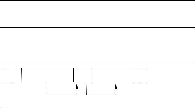
5 Defect Flagging Strategy
Media defects are remapped to the next available sector during the Format Process in manufacturing. The mapping from LBA to the physical locations is calculated by an internally maintained table.
5.1Shipped Format
Data areas are optimally used.
No extra sector is wasted as a spare throughout user data areas.
All pushes generated by defects are absorbed by the spare tracks of the inner zone.
N |
N+1 |
defect |
N+2 |
defect |
N+3 |
|
|
|
|
||
|
|
skip |
|
skip |
|
Figure 1 PList physical format
Defects are skipped without any constraint, such as track or cylinder boundary. The calculation from LBA to physical is done automatically by internal table.
12
Western Digital Hard Disk Drive OEM Specification

6 Specification
6.1Electrical Interface
6.1.1Connector Location
Refer to the following illustration to see the location of the connectors.
Figure 2 Connector location
Figure 3 Connector pin assignments
13
Western Digital Hard Disk Drive OEM Specification
6.1.1.1 Signal Connector (SATA)
A Serial ATA device may be either directly connected to a host or connected to a host through a cable.
For direct connection, the device plug connector is inserted directly into a backplane connector. The device plug connector and the backplane connector incorporate features that enable the direct connection to be hot pluggable and blind mated.
For connection via cable, the device signal plug connector mates with the signal cable receptacle connector on one end of the cable. The signal cable receptacle connector on the other end of the cable is inserted into a host signal plug connector. The signal cable wire consists of two twinax sections in a common outer sheath.
Besides the signal cable, there is also a separate power cable for the cabled connection. A Serial ATA power cable includes a power cable receptacle connector on one end and may be directly connected to the host power supply on the other end or may include a power cable receptacle on the other end. The power cable receptacle connector on one end of the power cable mates with the device power plug connector. The other end of the power cable is attached to the host as necessary.
14
Western Digital Hard Disk Drive OEM Specification
6.1.2Signal Definition (SATA)
SATA has receivers and drivers to be connected to TX+/- and RX +/- Serial data signal.
Defines the signal names of I/O connector pin and signal name.
|
No. |
|
Plug Connector Pin Definition |
Signal |
I/O |
|
S1 |
Gnd |
2nd mate |
Gnd |
|
|
S2 |
A+ |
Differential signal A from Phy |
RX+ |
Input |
|
S3 |
A- |
RX- |
Input |
|
|
|
||||
Signal |
S4 |
Gnd |
2nd mate |
Gnd |
|
|
|
|
|
|
|
|
S5 |
B- |
Differential signal B from Phy |
TX- |
Output |
|
S6 |
B+ |
TX+ |
Output |
|
|
|
||||
|
S7 |
Gnd |
2nd mate |
Gnd |
|
|
|
|
Key and spacing separate signal and power segments |
|
|
|
P1 |
Reserved* |
Not used (P1 and P2 tied internally) |
Reserve |
|
|
|
|
|
|
|
|
P2 |
Reserved* |
Not used (P1 and P2 tied internally) |
Reserve |
|
|
|
|
|
|
|
|
|
Reserved* or |
Not used (P1, P2, and P3 tied internally) |
Reserve |
|
|
P3 |
or |
or |
|
|
|
PWDIS* (option) |
|
|||
|
|
Enter/Exit Power Disable (option) |
PWDIS |
|
|
|
|
|
|
||
|
P4 |
Gnd |
1st mate |
Gnd |
|
|
P5 |
Gnd |
2nd mate |
Gnd |
|
|
|
|
|
|
|
|
P6 |
Gnd |
2nd mate |
Gnd |
|
|
|
|
|
|
|
Power |
P7 |
5V |
5V power, Precharge, 2nd Mate |
5V |
|
|
|
|
|
|
|
P8 |
5V |
5V power |
5V |
|
|
|
|
||||
|
|
|
|
|
|
|
P9 |
5V |
5V power |
5V |
|
|
P10 |
Gnd |
2nd mate |
Gnd |
|
|
|
|
|
|
|
|
P11 |
Reserved |
Support staggered spin-up and LED activity |
Reserve |
|
|
VDih max=2.1V |
|
|||
|
|
|
|
|
|
|
P12 |
Gnd |
1st mate |
Gnd |
|
|
|
|
|
|
|
|
P13 |
12V |
12V power, Precharge, 2nd mate |
12V |
|
|
P14 |
12V |
12V power |
12V |
|
|
P15 |
12V |
12V power |
12V |
|
|
|
|
|
|
|
Table 11 Interface Connector Pins and I/O Signals
* SATA Specification Revision 3.1 and prior revisions assigned 3.3V to pins P1, P2, and P3. In addition, device plug pins P1, P2, and P3 were required to be bused together. In the standard configuration of this product, P3 is connected with P1 and P2 and this product behaves as SATA 3.1 or prior version product in a system designed to SATA 3.2 system that does not support the 3.3 feature. For product with the optional SATA 3.3 Power Disable Feature supported, P3 is now assigned as the POWER DISABLE CONTROL PIN. If P3 is driven HIGH (2.1V-3.6V max), power to the drive circuitry will be disabled. Drives with this optional feature WILL NOT POWER UP in systems designed to SATA Spec Revision 3.1 or earlier because P3 driven HIGH will prevent the drive from powering up.
15
Western Digital Hard Disk Drive OEM Specification
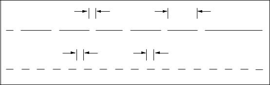
6.1.2.1 TX+ / TX- (SATA)
These signals are the outbound high-speed differential signals that are connected to the serial ATA cable
6.1.2.2 RX+ / RX- (SATA)
These signals are the inbound high-speed differential signals that are connected to the serial ATA cable.
6.1.2.3 5V Precharge
+5 Vdc that is available on the extended pins. It is used for Precharge when connected to backplane incorporated feature.
6.1.2.4 12V Precharge
+12 Vdc that is available on the extended pins. It is used for Precharge when connected to backplane incorporated feature.
6.1.3Out of Band Signaling (SATA)
COMRESET/COMINIT |
t1 |
t2 |
|
|
|
COMWAKE |
t3 |
t4 |
Figure 4 The timing of COMRESET, COMINIT and COMWAKE
|
|
PARAMETER DESCRIPTION |
Nominal (ns) |
|
|
|
|
t1 |
|
ALIGN primitives |
106.7 |
t2 |
|
Spacing |
320.0 |
t3 |
|
ALIGN primitives |
106.7 |
t4 |
|
Spacing |
106.7 |
Table 12 |
Parameter Descriptions |
|
|
6.1.4Voltage and Ground Signals
The 12V and 5V contacts provide all of the voltages required by the drive. The two voltages share a common ground plane to which all of the ground contacts are connected.
6.1.5Ready LED Output
The drive provides an open-drain driver with 15mA of current sink capability to the Ready LED Output signal. The cathode of the LED should be connected to this signal. The LED and the current -limiting resistor must be provided by the enclosure.
16
Western Digital Hard Disk Drive OEM Specification
Loading...