


S503T/S503TR/S503TRW
Vishay Telefunken
MOSMIC for TV±Tuner Prestage with 5 V Supply Voltage
MOSMIC - MOS Monolithic Integrated Circuit |
Electrostatic sensitive device. |
|
Observe precautions for handling. |
Applications
Low noise gain controlled input stages in UHF-and VHFtuner with 5 V supply voltage.
Features
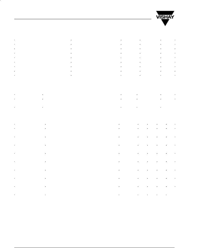
C block |
|
RFC |
|
|
VDD |
||
|
|
||
AGC |
G2 |
D |
|
C block |
|||
G1 |
RF out |
||
RF in |
C block |
||
S |
|||
|
|||
RG1 |
|
13650 |
|
|
|
VDD
DEasy Gate 1 switch-off with PNP switching transistors inside PLL
DHigh AGC-range with less steep slope
DIntegrated gate protection diodes
DLow noise figure
DHigh gain
DImproved cross modulation at gain reduction
DSMD package
2 |
1 |
1 |
2 |
94 9279 |
13 579 |
94 9278 |
95 10831 |
3 |
4 |
4 |
3 |
S503T Marking: 503 |
S503TR Marking: 53R |
||
Plastic case (SOT 143) |
Plastic case (SOT 143R) |
||
1 = Source, 2 = Drain, 3 = Gate 2, 4 = Gate 1 |
1 = Source, 2 = Drain, 3 = Gate 2, 4 = Gate 1 |
||
1 2
13 654 |
13 566 |
4 3
S503TRW Marking: W03 Plastic case (SOT 343R)
1 = Source, 2 = Drain, 3 = Gate 2, 4 = Gate 1
Document Number 85042 |
www.vishay.de •FaxBack +1-408-970-5600 |
Rev. 3, 20-Jan-99 |
1 (5) |
S503T/S503TR/S503TRW
Vishay Telefunken
Absolute Maximum Ratings
Tamb = 25_C, unless otherwise specified
Parameter |
Test Conditions |
Symbol |
Value |
Unit |
|
Drain - source voltage |
|
VDS |
8 |
V |
|
Drain current |
|
|
ID |
30 |
mA |
Gate 1/Gate 2 |
- source peak current |
|
±IG1/G2SM |
10 |
mA |
Gate 1/Gate 2 |
- source voltage |
|
±VG1/G2SM |
6 |
V |
Total power dissipation |
Tamb ≤ 60 °C |
Ptot |
200 |
mW |
|
Channel temperature |
|
TCh |
150 |
°C |
|
Storage temperature range |
|
Tstg |
±55 to +150 |
°C |
|
Maximum Thermal Resistance
Tamb = 25_C, unless otherwise specified
Parameter |
Test Conditions |
Symbol |
Value |
Unit |
Channel ambient |
on glass fibre printed board (25 x 20 x 1.5) mm3 |
R |
450 |
K/W |
|
plated with 35mm Cu |
thChA |
|
|
|
|
|
|
Electrical DC Characteristics
Tamb = 25_C, unless otherwise specified
Parameter |
Test Conditions |
Symbol |
Min |
Typ |
Max |
Unit |
Drain - source |
ID = 10 mA, VG2S = VG1S = 0 |
V(BR)DSS |
15 |
|
|
V |
breakdown voltage |
|
|
|
|
|
|
Gate 1 - source |
±IG1S = 10 mA, VG2S = VDS = 0 |
±V(BR)G1SS |
7 |
|
10 |
V |
breakdown voltage |
|
|
|
|
|
|
Gate 2 - source |
±IG2S = 10 mA, VG1S = VDS = 0 |
±V(BR)G2SS |
7 |
|
10 |
V |
breakdown voltage |
|
|
|
|
|
|
Gate 1 - source |
+VG1S = 5 V, VG2S = VDS = 0 |
+IG1SS |
|
|
20 |
nA |
leakage current |
|
|
|
|
|
|
Gate 2 - source |
±VG2S = 5 V, VG1S = VDS = 0 |
±IG2SS |
|
|
20 |
nA |
leakage current |
|
|
|
|
|
|
Drain - source |
VDS = VRG1 = 5 V, VG2S = 4 V, RG1 = 470 kW |
IDSO |
8 |
13 |
18 |
mA |
operating current |
|
|
|
|
|
|
Gate 1 - source |
VDS = 5 V, VG2S = 4, ID = 20 mA |
VG1S(OFF) |
0.3 |
|
1.0 |
V |
cut-off voltage |
|
|
|
|
|
|
Gate 2 - source |
VDS = VRG1 = 5 V, RG1 = 470 kW, ID = 20 mA |
VG2S(OFF) |
|
1.0 |
|
V |
cut-off voltage |
|
|
|
|
|
|
Remark on improving intermodulation behavior:
By setting RG1 smaller than 470 kW. e.g., 390 kW typical value of IDSO will raise and improved intermodulation behavior will be performed.
www.vishay.de •FaxBack +1-408-970-5600 |
Document Number 85042 |
2 (5) |
Rev. 3, 20-Jan-99 |
 Loading...