VISHAY TCMT1102, TCMT1101, TCMT1100, TCMT4100, TCMT1109 Datasheet
...
TCMT11.. Series
Vishay Semiconductors
Optocoupler with Phototransistor Output
Description
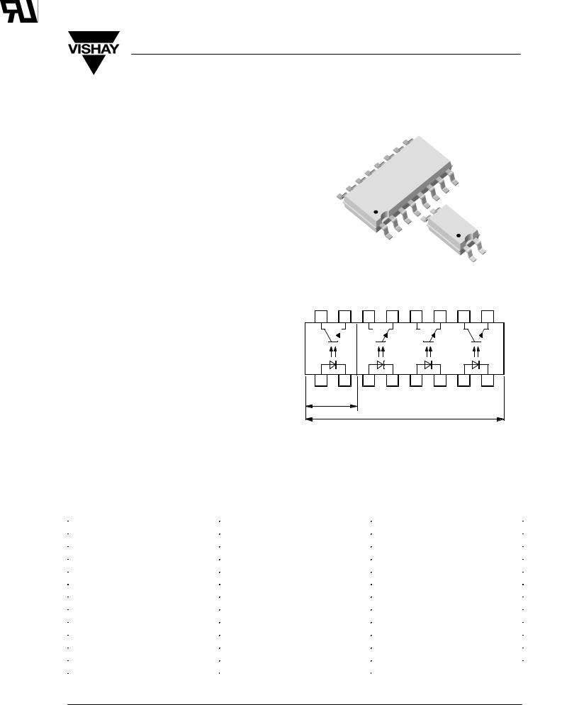
The TCMT11.. Series consist of a phototransistor optically coupled to a gallium arsenide infraredemitting diode in an 4- lead up to 16lead plastic Miniflat package.
The elements are mounted on one leadframe using a
16467
coplanar technique, providing a fixed distance between input and output for highest safety requirements.
Applications
Programmable logic controllers, modems, answering machines, general applications
Features
DLow profile package (half pitch)
DAC Isolation test voltage Vio = 3.75 kVRMS
DLow coupling capacitance of typical 0.3 pF
DCurrent Transfer Ratio (CTR) selected into groups
DLow temperature coefficient of CTR
DWide ambient temperature range
Coll. Emitter
9
16281
1 |
2 |
8 |
Anode Cath.
4 PIN
16 PIN
DUnderwriters Laboratory (UL) 1577 recognized, file number E-76222
DCSA (C-UL) 1577 recognized
file number E- 76222 - Double Protection
DCoupling System M
C
Order Instruction
Ordering Code |
CTR Ranking |
Remarks |
TCMT1100 |
50 to 600% |
4 Pin = Single channel |
TCMT1101 |
40 to 80% |
4 Pin = Single channel |
TCMT1102 |
63 to 125% |
4 Pin = Single channel |
TCMT1103 |
100 to 200% |
4 Pin = Single channel |
TCMT1104 |
160 to 320% |
4 Pin = Single channel |
TCMT1105 |
50 to 150% |
4 Pin = Single channel |
TCMT1106 |
100 to 300% |
4 Pin = Single channel |
TCMT1107 |
80 to 160% |
4 Pin = Single channel |
TCMT1108 |
130 to 260% |
4 Pin = Single channel |
TCMT1109 |
200 to 400% |
4 Pin = Single channel |
TCMT4100 |
50 to 600% |
16 Pin = Quad channel |
Document Number 83510 |
www.vishay.com |
Rev. A2, 15±Dec±00 |
1 (12) |

TCMT11.. Series
Vishay Semiconductors
Absolute Maximum Ratings
Input (Emitter)
Parameter |
Test Conditions |
Symbol |
Value |
Unit |
Reverse voltage |
|
VR |
6 |
V |
Forward current |
|
IF |
60 |
mA |
Forward surge current |
tp ≤ 10 ms |
IFSM |
1.5 |
A |
Power dissipation |
Tamb ≤ 25°C |
PV |
100 |
mW |
Junction temperature |
|
Tj |
125 |
°C |
Output (Detector)
Parameter |
Test Conditions |
Symbol |
Value |
Unit |
Collector emitter voltage |
|
VCEO |
70 |
V |
Emitter collector voltage |
|
VECO |
7 |
V |
Collector current |
|
IC |
50 |
mA |
Peak collector current |
tp/T = 0.5, tp ≤ 10 ms |
ICM |
100 |
mA |
Power dissipation |
Tamb ≤ 25°C |
PV |
150 |
mW |
Junction temperature |
|
Tj |
125 |
°C |
Coupler
Parameter |
Test Conditions |
Symbol |
Value |
Unit |
AC isolation test voltage (RMS) |
|
VIO 1) |
3.75 |
kV |
Total power dissipation |
Tamb ≤ 25°C |
Ptot |
250 |
mW |
Operating ambient temperature |
|
Tamb |
±40 to +100 |
°C |
range |
|
|
|
|
Storage temperature range |
|
Tstg |
±40 to +100 |
°C |
Soldering temperature |
|
Tsd |
235 |
°C |
1) Related to standard climate 23/50 DIN 50014
www.vishay.com |
Document Number 83510 |
2 (12) |
Rev. A2, 15±Dec±00 |

TCMT11.. Series
Vishay Semiconductors
Electrical Characteristics (Tamb = 25°C)
Input (Emitter)
Parameter |
Test Conditions |
Symbol |
Min. |
Typ. |
Max. |
Unit |
Forward voltage |
IF = 50 mA |
VF |
|
1.25 |
1.6 |
V |
Junction capacitance |
VR = 0 V, f = 1 MHz |
Cj |
|
50 |
|
pF |
Output (Detector)
Parameter |
Test Conditions |
Symbol |
Min. |
Typ. |
Max. |
Unit |
Collector emitter voltage |
IC = 100 mA |
VCEO |
70 |
|
|
V |
Emitter collector voltage |
IE = 100 mA |
VECO |
7 |
|
|
V |
Collector dark current |
VCE = 20 V, IF = 0, E = 0 |
ICEO |
|
|
100 |
nA |
Coupler
Parameter |
Test Conditions |
Symbol |
Min. |
Typ. |
Max. |
Unit |
Collector emitter saturation |
IF = 10 mA, IC = 1 mA |
VCEsat |
|
|
0.3 |
V |
voltage |
|
|
|
|
|
|
Cut-off frequency |
IF = 10 mA, VCE = 5 V, |
fc |
|
100 |
|
kHz |
|
RL = 100 W |
|
|
|
|
|
Coupling capacitance |
f = 1 MHz |
Ck |
|
0.3 |
|
pF |
Current Transfer Ratio (CTR)
Parameter |
Test Conditions |
Type |
Symbol |
Min. |
Typ. |
Max. |
Unit |
IC/IF |
VCE = 5 V, IF = 5 mA |
TCMT1100 |
CTR |
0.5 |
|
6.0 |
|
|
VCE = 5 V, IF = 10 mA |
TCMT1101 |
CTR |
0.4 |
|
0.8 |
|
|
VCE = 5 V, IF = 10 mA |
TCMT1102 |
CTR |
0.63 |
|
1.25 |
|
|
VCE = 5 V, IF = 10 mA |
TCMT1103 |
CTR |
1.0 |
|
2.0 |
|
|
VCE = 5 V, IF = 10 mA |
TCMT1104 |
CTR |
1.6 |
|
3.2 |
|
|
VCE = 5 V, IF = 5 mA |
TCMT1105 |
CTR |
0.5 |
|
1.5 |
|
|
VCE = 5 V, IF = 5 mA |
TCMT1106 |
CTR |
1.0 |
|
3.0 |
|
|
VCE = 5 V, IF = 5 mA |
TCMT1107 |
CTR |
0.8 |
|
1.6 |
|
|
VCE = 5 V, IF = 5 mA |
TCMT1108 |
CTR |
1.3 |
|
2.6 |
|
|
VCE = 5 V, IF = 5 mA |
TCMT1109 |
CTR |
2.0 |
|
4.0 |
|
|
VCE = 5 V, IF = 5 mA |
TCMT4100 |
CTR |
0.5 |
|
6.0 |
|
Document Number 83510 |
www.vishay.com |
Rev. A2, 15±Dec±00 |
3 (12) |

TCMT11.. Series
Vishay Semiconductors
Switching Characteristics
Parameter |
|
Test Conditions |
Symbol |
Typ. |
Unit |
Delay time |
VS = 5 |
V, IC = 2 mA, RL = 100 W (see figure 1) |
td |
3.0 |
ms |
Rise time |
|
|
tr |
3.0 |
ms |
Fall time |
|
|
tf |
4.7 |
ms |
Storage time |
|
|
ts |
0.3 |
ms |
Turn-on time |
|
|
ton |
6.0 |
ms |
Turn-off time |
|
|
toff |
5.0 |
ms |
Turn-on time |
VS = 5 |
V, IF = 10 mA, RL = 1 kW (see figure 2) |
ton |
9.0 |
ms |
Turn-off time |
|
|
toff |
18.0 |
ms |
IF IF
0
RG = 50 W
tp
T
= 0.01
tp = 50 ms
50 W
95 10804
 + 5 V
+ 5 V
 IC = 2 mA; adjusted through input amplitude
|
|
|
|
|
|
|
|
|
|
|
|
|
|
|
|
|
|
|
|
|
|
|
|
|
|
|
|
|
|
|
|
|
|
|
|
|
|
|
|
|
|
|
|
|
|
|
|
|
|
|
|
|
|
|
|
|
|
|
|
|
|
|
|
|
|
|
|
|
|
|
|
|
|
|
|
|
|
|
|
|
|
|
|
|
|
Channel I |
Oscilloscope |
||
|
|
|
|
|
|
|
|
|
|
|
|
|
|
|
|
|
|
|
|
|
|
|
|
|
|
|
|
|
|
|
|
Channel II |
RL = 1 MW |
||
100 W |
|
|
CL = 20 pF |
||||||||||||||
|
|
|
|
|
|
|
|
|
|
|
|
|
|
|
|
|
|
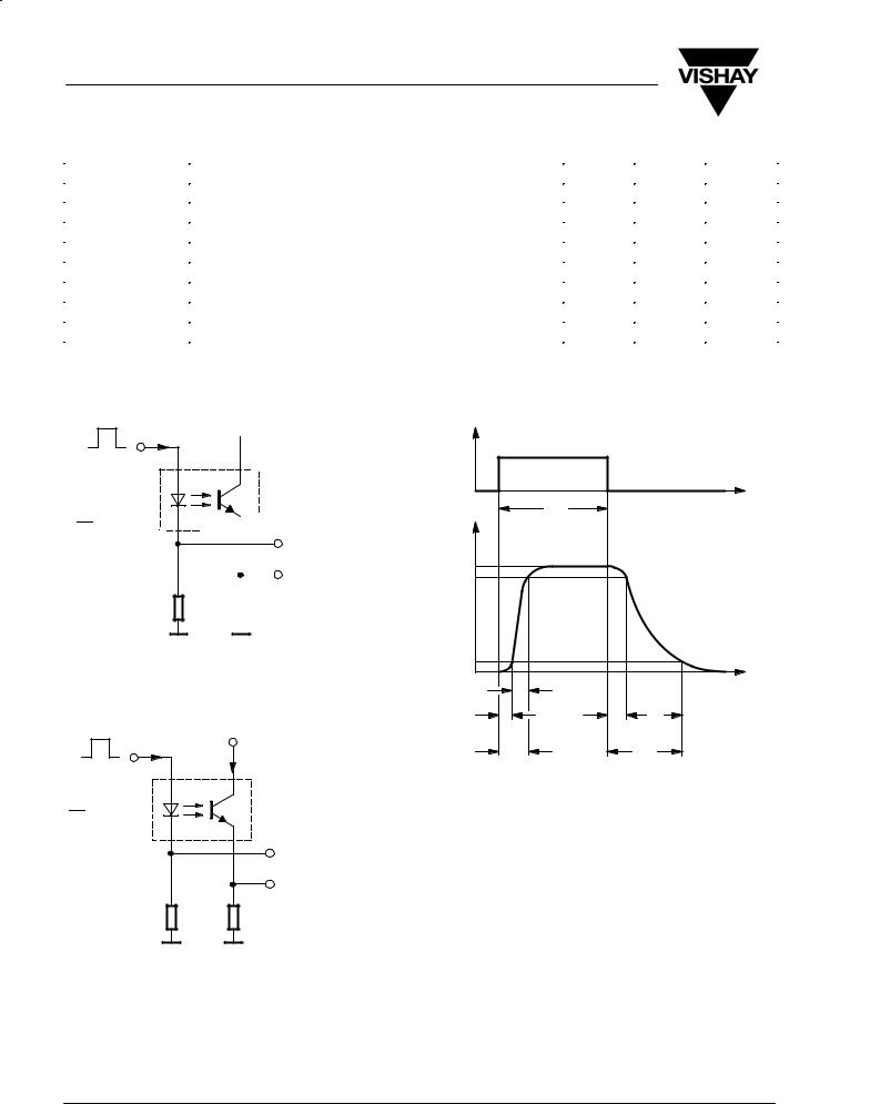
Figure 1. Test circuit, non-saturated operation
IF
0
RG = 50 W
tp
T
= 0.01
tp = 50 ms
95 10843
IF = 10 mA |
+ 5 V |
|
|
|
IC |
|
|
Channel I |
|
|
Channel II |
50 W |
1 kW |
|
Oscilloscope
RL > 1 MW CL < 20 pF
IF |
|
96 11698 |
|
|
|
0 |
|
t |
|
tp |
|
|
|
|
IC |
|
|
100% |
|
|
90% |
|
|
10% |
|
|
0 |
|
t |
tr |
|
|
|
|
|
td |
ts |
tf |
ton |
|
toff |
tp |
pulse duration |
ts |
storage time |
td |
delay time |
tf |
fall time |
tr |
rise time |
toff (= ts + tf) |
turn-off time |
ton (= td + tr) |
turn-on time |
|
|
Figure 3. Switching times
Figure 2. Test circuit, saturated operation
www.vishay.com |
Document Number 83510 |
4 (12) |
Rev. A2, 15±Dec±00 |
 Loading...