


Vishay DG408DJ, DG408DQ, DG408DY, DG409DJ, DG409DQ Schematics
...DG408, DG409
www.vishay.com |
Vishay Siliconix |
|
8-Ch/Dual 4-Ch High-Performance CMOS Analog Multiplexers
DESCRIPTION
The DG408 is an 8 channel single-ended analog multiplexer designed to connect one of eight inputs to a common output as determined by a 3-bit binary address (A0, A1, A2). The DG409 is a dual 4 channel differential analog multiplexer designed to connect one of four differential inputs to a common dual output as determined by its 2-bit binary address (A0, A1). Break-before-make switching action protects against momentary crosstalk between adjacent channels.
An on channel conducts current equally well in both directions. In the off state each channel blocks voltages up to the power supply rails. An enable (EN) function allows the user to reset the multiplexer/demultiplexer to all switches off for stacking several devices. All control inputs, address (Ax) and enable (EN) are TTL compatible over the full specified operating temperature range.
Applications for the DG408, DG409 include high speed data acquisition, audio signal switching and routing, ATE systems, and avionics. High performance and low power dissipation make them ideal for battery operated and remote instrumentation applications.
Designed in the 44 V silicon-gate CMOS process, the absolute maximum voltage rating is extended to 44 V. Additionally, single supply operation is also allowed. An epitaxial layer prevents latchup.
For additional information please see Technical Article TA201.
FEATURES
• Low on-resistance - RDS(on): 100
• Low charge injection - Q: 20 pC
• Fast transition time - tTRANS: 160 ns |
Available |
|
|
• Low power - ISUPPLY: 10 μA |
Available |
• Single supply capability |
|
•44 V supply max. rating
•TTL compatible logic
•Material categorization: For definitions of compliance please see www.vishay.com/doc?99912
Note
*This datasheet provides information about parts that are RoHS-compliant and/or parts that are non-RoHS-compliant. For example, parts with lead (Pb) terminations are not RoHS-compliant. Please see the information/tables in this datasheet for details.
BENEFITS
•Reduced switching errors
•Reduced glitching
•Improved data throughput
•Reduced power consumption
•Increased ruggedness
•Wide supply ranges
-Single supply: +5 V to 36 V
-Dual supplies: ± 5 V to ± 20 V
APPLICATIONS
•Data acquisition systems
•Audio signal routing
•ATE systems
•Battery powered systems
•Single supply systems
•Medical instrumentation
FUNCTIONAL BLOCK DIAGRAM AND PIN CONFIGURATION
DG408 Dual-In-Line,
SOIC and TSSOP
A0 |
1 |
|
16 |
A1 |
|
|
|
||
EN |
2 |
Decoders/Drivers |
15 |
A2 |
|
|
|||
V- |
3 |
|
14 |
GND |
|
|
|
||
S1 |
4 |
|
13 |
V+ |
|
|
|
||
S2 |
5 |
|
12 |
S5 |
|
|
|
||
S3 |
6 |
|
11 |
S6 |
|
|
|
||
S4 |
7 |
|
10 |
S7 |
|
|
|
||
D |
8 |
|
9 |
S8 |
|
|
|
Top View
DG409 Dual-In-Line,
SOIC and TSSOP
A0 |
1 |
|
16 |
A1 |
|
|
|
||
EN |
2 |
Decoders/Drivers |
15 |
GND |
|
|
|||
V- |
3 |
|
14 |
V+ |
|
|
|
||
S1a |
4 |
|
13 |
S1b |
|
|
|
||
S2a |
5 |
|
12 |
S2b |
|
|
|
||
S3a |
6 |
|
11 |
S3b |
|
|
|
||
S4a |
7 |
|
10 |
S4b |
|
|
|
||
Da |
8 |
|
9 |
Db |
Top View
S13-2504-Rev. K, 16-Dec-13 |
1 |
Document Number: 70062 |
|
For technical questions, contact: analogswitchtechsupport@vishay.com |
|
THIS DOCUMENT IS SUBJECT TO CHANGE WITHOUT NOTICE. THE PRODUCTS DESCRIBED HEREIN AND THIS DOCUMENT ARE SUBJECT TO SPECIFIC DISCLAIMERS, SET FORTH AT www.vishay.com/doc?91000

DG408, DG409
www.vishay.com
TRUTH TABLE (DG408)
A2 |
A1 |
A0 |
EN |
ON SWITCH |
X |
X |
X |
0 |
None |
|
|
|
|
|
0 |
0 |
0 |
1 |
1 |
|
|
|
|
|
0 |
0 |
1 |
1 |
2 |
|
|
|
|
|
0 |
1 |
0 |
1 |
3 |
|
|
|
|
|
0 |
1 |
1 |
1 |
4 |
|
|
|
|
|
1 |
0 |
0 |
1 |
5 |
|
|
|
|
|
1 |
0 |
1 |
1 |
6 |
|
|
|
|
|
1 |
1 |
0 |
1 |
7 |
|
|
|
|
|
1 |
1 |
1 |
1 |
8 |
|
|
|
|
|
Vishay Siliconix
TRUTH TABLE (DG409)
A1 |
A0 |
EN |
ON SWITCH |
X |
X |
0 |
None |
|
|
|
|
0 |
0 |
1 |
1 |
|
|
|
|
0 |
1 |
1 |
2 |
|
|
|
|
1 |
0 |
1 |
3 |
|
|
|
|
1 |
1 |
1 |
4 |
|
|
|
|
Notes
•Logic “0” = VAL 0.8 V
•Logic “1” = VAH 2.4 V
•X = Do not care
ORDERING INFORMATION (Commercial)
PART |
CONFIGURATION |
TEMP. RANGE |
PACKAGE |
ORDERING PART NUMBER |
|
|
|
|
|
|
|
|
|
|
16-pin plastic DIP |
DG408DJ |
|
|
|
|
|
||
|
|
|
DG408DJ-E3 |
||
|
|
|
|
||
|
|
|
|
|
|
|
|
|
|
DG408DY |
|
|
|
|
|
|
|
DG408 |
8:1 x 1 |
-40 °C to 85 °C |
16-pin SOIC |
DG408DY-E3 |
|
|
|||||
DG408DY-T1 |
|||||
|
|
|
|
||
|
|
|
|
|
|
|
|
|
|
DG408DY-T1-E3 |
|
|
|
|
|
|
|
|
|
|
16-pin TSSOP |
DG408DQ-E3 |
|
|
|
|
|
||
|
|
|
DG408DQ-T1-E3 |
||
|
|
|
|
||
|
|
|
|
|
|
|
|
|
16-pin plastic DIP |
DG409DJ |
|
|
|
|
|
||
|
|
|
DG409DJ-E3 |
||
|
|
|
|
||
|
|
|
|
|
|
|
|
|
|
DG409DY |
|
|
|
|
|
|
|
DG409 |
4:1 x 2 |
-40 °C to 85 °C |
16-pin SOIC |
DG409DY-E3 |
|
|
|||||
DG409DY-T1 |
|||||
|
|
|
|
||
|
|
|
|
|
|
|
|
|
|
DG409DY-T1-E3 |
|
|
|
|
|
|
|
|
|
|
16-pin TSSOP |
DG409DQ-E3 |
|
|
|
|
|
||
|
|
|
DG409DQ-T1-E3 |
||
|
|
|
|
||
|
|
|
|
|
|
Note |
|
|
|
|
• -T1 indicates Tape and Reel, -E3 indicates Lead-Free and RoHS Compliant, NO -E3 indicates standard Tin/Lead finish.
ABSOLUTE MAXIMUM RATINGS
PARAMETER |
|
LIMIT |
UNIT |
|
|
|
|
|
|
Voltages Referenced to V- |
V+ to V- e |
44 |
|
|
GND to V- |
-25 |
V |
||
|
||||
|
|
|
||
Digital Inputsa, VS, VD |
|
(V-) - 2 to (V+) + 2 |
||
|
|
|||
|
or 20 mA, whichever occurs first |
|
||
|
|
|
||
|
|
|
|
|
Current (any terminal) |
|
30 |
mA |
|
|
|
|
||
Peak Current, S or D (pulsed at 1 ms, 10 % duty cycle max.) |
100 |
|||
|
||||
|
|
|
|
|
Storage Temperature |
(DJ, DY suffix) |
-65 to 125 |
°C |
|
|
|
|
|
|
Power Dissipation (Package) b |
16-pin plastic DIP c |
450 |
mW |
|
16-pin narrow SOIC and TSSOP d |
600 |
|||
|
|
|||
Notes
a.Signals on SX, DX or INX exceeding V+ or V- will be clamped by internal diodes. Limit forward diode current to maximum current ratings.
b.All leads soldered or welded to PC board.
c.Derate 6 mW/°C above 75 °C.
d.Derate 7.6 mW/°C above 75 °C.
e.Also applies when V- = GND.
S13-2504-Rev. K, 16-Dec-13 |
2 |
Document Number: 70062 |
|
For technical questions, contact: analogswitchtechsupport@vishay.com |
|
THIS DOCUMENT IS SUBJECT TO CHANGE WITHOUT NOTICE. THE PRODUCTS DESCRIBED HEREIN AND THIS DOCUMENT ARE SUBJECT TO SPECIFIC DISCLAIMERS, SET FORTH AT www.vishay.com/doc?91000

|
|
|
|
|
|
|
|
DG408, DG409 |
|||
|
|
|
|
|
|
|
|
||||
|
|
|
www.vishay.com |
|
|
|
Vishay Siliconix |
||||
|
|
|
|
|
|
|
|
||||
|
|
|
|
|
|
|
|
|
|||
SPECIFICATIONS a |
|
|
|
|
|
|
|
||||
|
|
|
|
|
TEST CONDITIONS UNLESS |
|
|
D SUFFIX |
|
||
|
|
|
|
|
OTHERWISE SPECIFIED |
|
|
-40 °C to 85 °C |
|
||
|
|
|
|
|
|
|
|
|
|
|
|
|
|
|
|
|
V+ = 15 V, V- = -15 V |
|
|
|
|
|
|
|
|
|
TEMP. b |
TYP. c |
MIN. d |
MAX. d |
|
||||
PARAMETER |
SYMBOL |
VAL = 0.8 V, VAH = 2.4 Vf |
UNIT |
||||||||
Analog Switch |
|
|
|
|
|
|
|
||||
Analog Signal Range e |
VANALOG |
|
Full |
- |
-15 |
15 |
V |
||||
Drain-Source |
RDS(on) |
VD = ± 10 V, IS = -10 mA |
Room |
40 |
- |
100 |
|
||||
On-Resistance |
Full |
- |
- |
125 |
|
||||||
|
|
||||||||||
|
|
|
|
|
|
|
|
|
|
||
RDS(on) Matching Between |
RDS(on) |
VD = ± 10 V |
Room |
- |
- |
15 |
|||||
|
|||||||||||
Channels g |
|
||||||||||
|
|
|
|
|
|
|
|||||
Source Off Leakage Current |
IS(off) |
VS = ± 10 V, |
Room |
- |
-0.5 |
0.5 |
|
||||
VD = ± 10 V, VEN = 0 V |
Full |
- |
-5 |
5 |
|
||||||
|
|
|
|
|
|
||||||
DG408 |
|
|
|
|
Room |
- |
-1 |
1 |
|
||
|
|
|
|
|
VD = ± 10 V, |
|
|
|
|
|
|
DG408 |
Drain Off Leakage |
ID(off) |
Full |
- |
-20 |
20 |
|
||||
VS = ± 10 V, |
|
||||||||||
DG409 |
Current |
Room |
- |
-1 |
1 |
|
|||||
|
VEN = 0 V |
nA |
|||||||||
|
|
|
|
|
|
|
|
|
|||
DG409 |
|
|
|
Full |
- |
-10 |
10 |
||||
|
|
|
|
||||||||
|
|
|
|
|
|||||||
|
|
|
|
|
|
|
|
|
|
||
DG408 |
|
|
|
|
Room |
- |
-1 |
1 |
|
||
|
|
|
|
|
VS = VD = ± 10 V |
|
|
|
|
|
|
DG408 |
Drain On Leakage |
ID(on) |
Full |
- |
-20 |
20 |
|
||||
sequence each |
|
||||||||||
DG409 |
Current |
Room |
- |
-1 |
1 |
|
|||||
|
switch on |
|
|||||||||
|
|
|
|
|
|
|
|
|
|
||
DG409 |
|
|
|
|
Full |
- |
-10 |
10 |
|
||
|
|
|
|
|
|
|
|
|
|||
Digital Control |
|
|
|
|
|
|
|
||||
Logic High Input Voltage |
VINH |
|
Full |
- |
2.4 |
- |
V |
||||
Logic Low Input Voltage |
VINL |
|
Full |
- |
- |
0.8 |
|||||
|
|
||||||||||
Logic High Input Current |
IAH |
VA = 2.4 V, 15 V |
Full |
- |
-10 |
10 |
μA |
||||
Logic Low Input Current |
IAL |
VEN = 0 V, 2.4 V, VA = 0 V |
Full |
- |
-10 |
10 |
|||||
|
|||||||||||
Logic Input Capacitance |
Cin |
f = 1 MHz |
Room |
8 |
- |
- |
pF |
||||
Dynamic Characteristics |
|
|
|
|
|
|
|
||||
Transition Time |
tTRANS |
see figure 2 |
Full |
160 |
- |
250 |
|
||||
Break-Before-Make Interval |
tOPEN |
see figure 4 |
Room |
- |
10 |
- |
|
||||
Enable Turn-On Time |
tON(EN) |
|
Room |
115 |
- |
150 |
ns |
||||
|
|
|
|
|
|
||||||
see figure 3 |
Full |
- |
- |
- |
|
||||||
|
|
|
|
|
|
||||||
|
|
|
|
|
|
|
|
||||
Enable Turn-Off Time |
tOFF(EN) |
|
Room |
105 |
- |
150 |
|
||||
Charge Injection |
Q |
CL = 10 nF, VS = 0 V |
Room |
20 |
- |
- |
pC |
||||
Off Isolation h |
OIRR |
VEN = 0 V, RL = 1 k , |
Room |
-75 |
- |
- |
|
||||
|
|
|
|
|
f = 1 MHz |
|
|
|
|
|
|
Source Off Capacitance |
CS(off) |
VEN = 0 V, VS = 0 V, |
Room |
3 |
- |
- |
|
||||
f = 1 MHz |
|
||||||||||
|
|
|
|
|
|
|
|
|
|
||
|
|
|
|
|
|
|
|
|
|
pF |
|
DG408 |
Drain Off |
CD(off) |
VEN = 0 V, |
Room |
26 |
- |
- |
||||
|
|||||||||||
DG409 |
Capacitance |
Room |
14 |
- |
- |
|
|||||
|
|
|
|
|
VD = 0 V, |
|
|
|
|
|
|
DG408 |
Drain On |
|
Room |
37 |
- |
- |
|
||||
CD(on) |
f = 1 MHz |
|
|||||||||
DG409 |
Capacitance |
|
Room |
25 |
- |
- |
|
||||
|
|
|
|||||||||
|
|
|
|
|
|
|
|
|
|||
Power Supplies |
|
|
|
|
|
|
|
||||
Positive Supply Current |
I+ |
VEN = VA = 0 V or 5 V |
Full |
10 |
- |
75 |
μA |
||||
|
|
|
|
|
|
|
|
|
|||
Negative Supply Current |
I- |
Full |
1 |
-75 |
- |
||||||
|
|
||||||||||
|
|
|
|
|
|
|
|
|
|
|
|
Positive Supply Current |
I+ |
|
Room |
0.2 |
- |
0.5 |
mA |
||||
VEN = VA = 0 V or 5 V |
|
|
|
|
|||||||
Full |
- |
- |
2 |
||||||||
|
|
|
|
|
|
||||||
Negative Supply Current |
I- |
|
Full |
- |
-500 |
- |
μA |
||||
|
|
|
|
|
|
|
|
|
|
|
|
S13-2504-Rev. K, 16-Dec-13 |
3 |
Document Number: 70062 |
|
For technical questions, contact: analogswitchtechsupport@vishay.com |
|
THIS DOCUMENT IS SUBJECT TO CHANGE WITHOUT NOTICE. THE PRODUCTS DESCRIBED HEREIN AND THIS DOCUMENT ARE SUBJECT TO SPECIFIC DISCLAIMERS, SET FORTH AT www.vishay.com/doc?91000

|
|
|
|
|
|
|
DG408, DG409 |
|||
|
|
|
|
|
|
|
||||
|
|
www.vishay.com |
|
|
|
Vishay Siliconix |
||||
|
|
|
|
|
|
|
||||
|
|
|
|
|
|
|
|
|||
SPECIFICATIONSa (Single Supply) |
|
|
|
|
|
|||||
|
|
|
|
TEST CONDITIONS UNLESS |
|
|
D SUFFIX |
|
||
|
|
|
|
OTHERWISE SPECIFIED |
|
|
-40 °C to 85 °C |
|
||
|
|
|
|
|
|
|
|
|
|
|
|
|
|
|
V+ = 12 V, V- = 0 V |
|
|
|
|
|
|
|
|
|
TEMP. b |
TYP. c |
MIN. d |
MAX. d |
|
|||
PARAMETER |
SYMBOL |
VAL = 0.8 V, VAH = 2.4 Vf |
UNIT |
|||||||
Analog Switch |
|
|
|
|
|
|
|
|||
Drain-Source |
RDS(on) |
VD = 3 V, 10 V, IS = -1 mA |
Room |
90 |
- |
- |
|
|||
On-Resistance e,f |
||||||||||
|
|
|
|
|
|
|
||||
Dynamic Characteristics |
|
|
|
|
|
|
|
|||
Switching Time of |
tTRANS |
VS1 = 8 V, VS8 = 0 V, VIN = 2.4 V |
Room |
180 |
- |
- |
|
|||
Multiplexer e |
|
|||||||||
Enable Turn-On Time e |
tON(EN) |
VINH = 2.4 V, VINL = 0 V, |
Room |
180 |
- |
- |
ns |
|||
|
|
|
|
VS1 = 5 V |
|
|
|
|
|
|
Enable Turn-Off Time e |
tOFF(EN) |
|
Room |
120 |
- |
- |
|
|||
Charge Injection e |
Q |
CL = 1 nF, VS = 0 V, RS = 0 |
Room |
5 |
- |
- |
pC |
|||
Notes
a.Refer to PROCESS OPTION FLOWCHART.
b.Room = 25 °C, Full = as determined by the operating temperature suffix.
c.Typical values are for DESIGN AID ONLY, not guaranteed nor subject to production testing.
d.The algebraic convention whereby the most negative value is a minimum and the most positive a maximum, is used in this datasheet.
e.Guaranteed by design, not subject to production test.
f.VIN = input voltage to perform proper function.
g.RDS(on) = RDS(on) max. - RDS(on) min.
h.Worst case isolation occurs on channel 4 due to proximity to the drain pin.
Stresses beyond those listed under “Absolute Maximum Ratings” may cause permanent damage to the device. These are stress ratings only, and functional operation of the device at these or any other conditions beyond those indicated in the operational sections of the specifications is not implied. Exposure to absolute maximum rating conditions for extended periods may affect device reliability.
S13-2504-Rev. K, 16-Dec-13 |
4 |
Document Number: 70062 |
|
For technical questions, contact: analogswitchtechsupport@vishay.com |
|
THIS DOCUMENT IS SUBJECT TO CHANGE WITHOUT NOTICE. THE PRODUCTS DESCRIBED HEREIN AND THIS DOCUMENT ARE SUBJECT TO SPECIFIC DISCLAIMERS, SET FORTH AT www.vishay.com/doc?91000
DG408, DG409
www.vishay.com |
Vishay Siliconix |
|
|
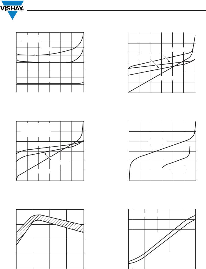
TYPICAL CHARACTERISTICS (25 °C, unless otherwise noted) |
|
CS, D (pF)
80 |
|
|
|
|
|
|
|
60 |
|
|
|
|
|
|
|
V+ = 15 V |
|
|
|
|
|
|
VS = 0 V for ID(off) |
|
|
|
|
||
|
V- = - 15 V |
|
|
|
|
|
|
VS = VD for ID(on) |
|
|
|
|
||
|
|
|
|
|
|
|
|
40 |
|
|
|
|
|
|
60 |
|
|
CD(on) |
|
|
|
|
|
|
|
|
DG408 I |
|
|
|
|
|
|
|
|
|
|
|
|
|
|
|
||
|
|
|
|
|
|
|
|
|
|
|
|
D(off) |
|
|
|
|
|
|
|
|
|
|
20 |
|
DG409 ID(off) |
|
|
|
|
|
|
|
CD(off) |
|
|
|
(pA) |
|
DG409 ID(on) |
|
|
|
|
|
40 |
|
|
|
|
|
|
0 |
|
|
|
|
|
|
|
|
|
|
|
|
|
D |
|
|
|
|
|
|
||
|
|
|
|
|
|
|
|
|
|
|
|
|
|
|
|
|
|
|
|
|
|
I |
|
|
|
|
|
|
|
|
|
|
|
|
|
|
|
- 20 |
|
|
|
|
|
|
20 |
|
|
CS(off) |
|
|
|
|
|
|
|
DG408 ID(on) |
|
|
|
|
|
|
|
|
|
|
- 40 |
|
|
|
|
|
|
|
|
|
|
|
|
|
|
|
|
|
|
|
|
|
|
0 |
|
|
|
|
|
|
|
- 60 |
|
|
|
|
|
|
- 15 |
- 10 |
- 5 |
0 |
5 |
10 |
15 |
|
0 |
2 |
4 |
6 |
8 |
10 |
12 |
|
|
VANALOG - Analog Voltage (V) |
|
|
|
|
|
VANALOG - Analog Voltage (V) |
|
|
||||
Source/Drain Capacitance vs. Analog Voltage |
Drain Leakage Current vs. Source/Drain Voltage |
|
(Single 12 V Supply) |
|
100 |
V+ = 15 V |
|
|
|
|
|
|
|
|
|
|
|
||
|
|
V- = - 15 V |
|
|
|
|
|
|
60 |
VS = - VD for ID(off) |
|
|
|
|
|
|
|
VD = VS(open) for ID(on) |
|
|
|
||
|
20 |
|
DG409 ID(off) |
|
|
|
|
|
|
|
|
|
|
||
(pA) |
- 20 |
|
|
|
|
|
|
D |
|
|
|
|
|
|
|
|
|
|
|
|
|
|
|
I |
|
|
|
|
|
|
|
|
- 60 |
|
|
|
DG409 ID(on) |
|
|
|
- 100 |
|
DG408 ID(on), ID(off) |
|
|
||
|
- 140 |
|
|
|
|
|
|
|
- 15 |
- 10 |
- 5 |
0 |
5 |
10 |
15 |
|
|
VD or VS - Drain or Source Voltage (V) |
|
||||
Drain Leakage Current vs. Source/Drain Voltage
|
2.0 |
|
|
|
|
|
1.5 |
|
|
|
|
(V) |
1.0 |
|
|
|
|
TH |
|
|
|
|
|
|
|
|
|
|
|
V |
|
|
|
|
|
|
0.5 |
|
|
|
|
|
0.0 |
|
|
|
|
|
4 |
8 |
12 |
16 |
20 |
+ VSUPPLY (V)
|
20 |
|
|
|
|
|
|
|
15 |
|
|
|
|
|
|
|
10 |
|
V+ = 15 V |
|
|
|
|
|
|
V- = - 15 V |
|
|
|
||
(pA) |
5 |
|
|
|
|
|
|
S(off) |
|
|
|
|
|
|
|
|
|
|
|
|
|
|
|
I |
|
|
|
|
|
|
|
|
0 |
|
|
|
|
|
|
|
|
|
|
|
V+ = 12 V |
|
|
|
- 5 |
|
|
|
V- = 0 V |
|
|
|
|
|
|
|
|
|
|
|
- 10 |
|
|
|
|
|
|
|
- 15 |
- 10 |
- 5 |
0 |
5 |
10 |
15 |
|
|
|
VS - Source Voltage (V) |
|
|
||
Source Leakage Current vs. Source Voltage
- 100 mA
VSUPPLY = ± 15 V
-10 mA
-1 mA
|
|
|
|
|
|
VEN = 2.4 V |
|
|
|
|
|
|
||
I- |
|
|
|
|
|
|
|
|
|
|
|
|
|
|
|
- 100 |
µA |
|
|
|
|
|
|
|
|
|
|
|
|
|
- 10 |
µA |
|
|
|
|
|
|
|
|
|
|
|
|
|
|
|
|
|
|
|
|
|
|
|
|
|||
|
|
|
|
|
|
|
|
|
VEN = 0 V or 5 V |
|
|
|||
|
- 1 µA |
|
|
|
|
|
|
|
|
|
|
|
|
|
|
- 0.1 |
µA |
|
|
|
|
|
|
|
|
|
|
|
|
|
|
|
|
|
|
|
|
|
|
|
|
|
||
|
|
100 |
1K |
10K |
100K |
1M |
10M |
|||||||
|
|
|
|
|
|
Switching Frequency (Hz) |
|
|
|
|
||||
Input Switching Threshold vs. Supply Voltage |
Negative Supply Current vs. Switching Frequency |
|
|
||
|
|
|
S13-2504-Rev. K, 16-Dec-13 |
5 |
Document Number: 70062 |
|
For technical questions, contact: analogswitchtechsupport@vishay.com |
|
THIS DOCUMENT IS SUBJECT TO CHANGE WITHOUT NOTICE. THE PRODUCTS DESCRIBED HEREIN AND THIS DOCUMENT ARE SUBJECT TO SPECIFIC DISCLAIMERS, SET FORTH AT www.vishay.com/doc?91000

DG408, DG409
www.vishay.com |
Vishay Siliconix |
|
TYPICAL CHARACTERISTICS (25 °C, unless otherwise noted)
100 mA |
|
|
|
|
|
100 µA |
|
|
|
|
|
|
|
|
|
|
|
|
VSUPPLY = 15 V |
|
|
|
10 µA |
|
|
|
|
|
|
|
|
|
|
|
|
|
|
|
|
|
I+ |
|
|
|
|
|
|
|
|
|
|
10 mA |
|
|
|
|
|
1 µA |
|
|
|
|
|
|
|
|
|
|
|
|
|
|
|
|
|
|
|
|
|
|
|
|
|
|
|
|
|
VEN = 2.4 V |
|
|
100 nA |
|
|
|
|
|
|
|
|
|
|
I+ |
|
|
|
|
|
|
- |
|
|
|
|
|
|
|
|
|
1 mA |
|
|
|
|
|
I+,I |
|
|
|
|
|
|
|
|
|
|
|
|
|
|
|
|
|
|
|
|
|
|
|
|
|
|
|
|
|
|
|
|
|
|
10 nA |
|
|
|
|
|
|
|
|
|
|
100 µA |
|
|
|
|
|
1 nA |
|
|
|
|
|
|
|
|
|
|
|
|
|
|
|
|
- (I-) |
|
|
|
VSUPPLY = ± 15 V |
|
||||
|
|
|
|
|
|
|
|
|
|
|
|
|||||
|
|
|
|
VEN = 0 V or 5 V |
|
100 pA |
|
|
|
|
VA = 0 V |
|
|
|
||
|
|
|
|
|
|
|
|
|
|
|
|
VEN = 0 V |
|
|
|
|
|
10 µA |
|
|
|
|
|
10 pA |
|
|
|
|
|
|
|
|
|
|
100 |
1K |
10K |
100K |
1M |
10M |
- 55 |
- 35 |
- 15 |
5 |
25 |
45 |
65 |
85 |
105 |
125 |
|
|
|
Switching Frequency (Hz) |
|
|
|
|
|
|
Temperature (°C) |
|
|
|
|||
Positive Supply Current vs. Switching Frequency |
ISUPPLY vs. Temperature |
I+ (µA)
|
|
|
|
|
|
|
|
|
|
90 |
|
|
|
|
|
|
20 |
|
|
|
|
|
|
|
|
|
80 |
CL = 10 000 pF |
|
|
|
|
|
|
|
|
|
|
|
|
|
|
VIN = 5 Vp-p |
|
|
|
|
|||
|
|
|
|
|
|
|
|
|
|
|
|
|
|
|
||
|
|
|
|
|
|
|
|
|
|
70 |
|
|
|
|
|
|
15 |
|
|
|
|
|
|
|
|
|
60 |
|
|
|
|
|
|
|
|
|
|
|
|
|
|
|
|
|
|
|
|
|
|
|
|
V+ = 15 V |
|
|
|
|
|
|
|
(pC) |
50 |
|
|
V+ = 15 V |
|
|
|
|
|
|
|
|
|
|
|
40 |
|
|
V- = - 15 V |
|
|
|
||
|
|
|
|
|
|
|
|
|
|
|
|
|
|
|
|
|
10 |
V- = - 15 V |
|
|
|
|
|
|
|
Q |
|
|
|
|
|
|
|
|
VIN = 0 V |
|
|
|
|
|
|
|
|
30 |
|
|
|
|
|
|
|
VEN = 0 V |
|
|
|
|
|
|
|
|
20 |
|
|
|
|
|
|
|
|
|
|
|
|
|
|
|
|
|
|
|
|
|
|
|
5 |
|
|
|
|
|
|
|
|
|
10 |
|
|
|
|
|
|
|
|
|
|
|
|
|
|
|
|
|
|
|
|
|
|
|
|
|
|
|
|
|
|
|
|
|
0 |
|
|
|
|
V+ = 12 V |
|
|
|
|
|
|
|
|
|
|
|
|
|
|
|
V- = 0 V |
|
|
|
|
|
|
|
|
|
|
|
|
|
|
|
|
|
|
|
0 |
|
|
|
|
|
|
|
|
|
- 10 |
|
|
|
|
|
|
- 55 |
- 35 - 15 |
5 |
25 |
45 |
65 |
85 |
105 |
125 |
|
- 15 |
- 10 |
- 5 |
0 |
5 |
10 |
15 |
|
|
Temperature (°C) |
|
|
|
|
|
|
VS - Source Voltage (V) |
|
|
|||||
Positive Supply Current vs. Temperature (DG408) |
Charge Injection vs. Analog Voltage |
|
120 |
|
|
|
|
|
|
|
|
|
|
|
100 |
|
|
|
|
|
|
± 5 V |
|
|
|
|
|
|
|
|
|
|
|
|
|
||
|
80 |
|
|
|
|
|
|
|
|
|
|
(Ω) |
|
|
|
|
|
|
|
|
± 8 V |
|
|
DS(on) |
60 |
|
|
|
|
|
|
|
± 10 V |
|
|
|
|
|
|
|
|
|
|
|
|||
|
|
|
|
|
|
|
|
|
± 12 V |
|
|
R |
40 |
|
|
|
|
|
|
|
|
|
|
|
|
|
|
|
|
|
|
|
|
|
|
|
20 |
|
|
± 20 V |
|
± 15 V |
|
|
|
|
|
|
|
|
|
|
|
|
|
|
|||
|
0 |
|
|
|
|
|
|
|
|
|
|
|
- 20 |
- 16 |
- 12 |
- 8 |
- 4 |
0 |
4 |
8 |
12 |
16 |
20 |
|
|
|
|
VD - Drain Voltage (V) |
|
|
|
||||
|
160 |
|
|
|
140 |
|
|
|
|
V+ = 7.5 V |
|
|
120 |
|
|
Ω) |
100 |
10 V |
|
|
|
|
|
( |
|
|
|
DS(on) |
80 |
12 V |
|
|
|
||
|
|
|
|
R |
60 |
15 V |
20 V |
|
|
|
|
|
40 |
|
22 V |
|
|
V- = 0 V |
|
|
20 |
|
|
0
0 |
4 |
8 |
12 |
16 |
20 |
22 |
|
|
VD - Drain Voltage (V) |
|
|
|
|
RDS(on) vs. VD and Supply |
RDS(on) vs. VD and Supply (Single Supply) |
|
S13-2504-Rev. K, 16-Dec-13 |
6 |
Document Number: 70062 |
|
For technical questions, contact: analogswitchtechsupport@vishay.com |
|
THIS DOCUMENT IS SUBJECT TO CHANGE WITHOUT NOTICE. THE PRODUCTS DESCRIBED HEREIN AND THIS DOCUMENT ARE SUBJECT TO SPECIFIC DISCLAIMERS, SET FORTH AT www.vishay.com/doc?91000
 Loading...