


SST5460
Vishay SST5460, SST5461, SST5462, 2N5460, 2N5461 Schematic [ru]
...
2N/SST5460 Series
Vishay Siliconix
Document Number: 70262
S-04030—Rev. D, 04-Jun-01
www.vishay.com
9-1
P-Channel JFETs
2N5460 SST5460
2N5461 SST5461
2N5462 SST5462
PRODUCT SUMMARY
Part Number V
GS(off)
(V) V
(BR)GSS
Min (V) g
fs
Min (mS) I
DSS
Min (mA)
2N/SST5460 0.75 to 6 40 1 –1
2N/SST5461 1 to 7.5 40 1.5 –2
2N/SST5462 1.8 to 9 40 2 –4
FEATURES BENEFITS APPLICATIONS
D High Input Impedance
D Very Low Noise
D High Gain: A
V
= 80 @ 20 mA
D Low Capacitance: 1.2 pF Typical
D Low Signal Loss/System Error
D High System Sensitivity
D High-Quality Low-Level Signal
Amplification
D Low-Current, Low-Voltage Amplifiers
D High-Side Switching
D Ultrahigh Input Impedance
Pre-Amplifiers
DESCRIPTION
The 2N/SST5460 series are p-channel JFETs designed to
provide all-around performance in a wide range of amplifier
and analog switch applications.
The 2N series, TO-226AA (TO-92), and SST series, TO-236
(SOT-23), plastic packages provide low cost options, and are
available in tape-and-reel for automated assembly, (see
Packaging Information).
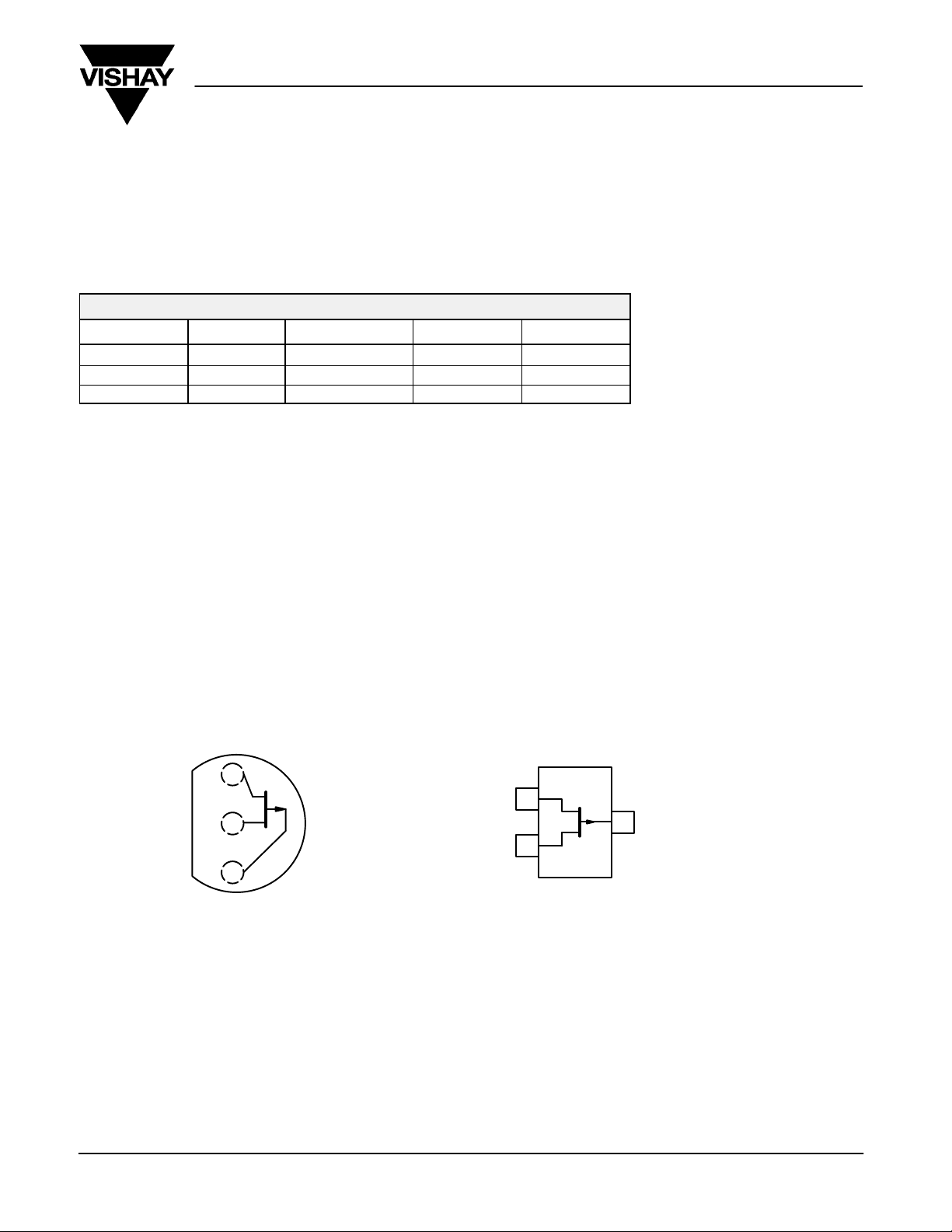
TO-226AA
(TO-92)
Top View
S
G
D
1
2
3
D
S
G
TO-236
(SOT-23)
2
3
1
SST5460 (B0)*
SST5461 (B1)*
SST5462 (B2)*
*Marking Code for TO-236
Top View
2N5460
2N5461
2N5462
ABSOLUTE MAXIMUM RATINGS
Gate-Drain Voltage 40 V. . . . . . . . . . . . . . . . . . . . . . . . . . . . . . . . . . . . . . . . . . . . .
Gate-Source Voltage 40 V. . . . . . . . . . . . . . . . . . . . . . . . . . . . . . . . . . . . . . . . . . . .
Gate Current –10 mA. . . . . . . . . . . . . . . . . . . . . . . . . . . . . . . . . . . . . . . . . . . . . . . .
Storage Temperature –65 to 150_C. . . . . . . . . . . . . . . . . . . . . . . . . . . . . . . . . . .
Operating Junction Temperature –55 to 150_C. . . . . . . . . . . . . . . . . . . . . . . . . .
Lead Temperature (
1
/
16
” from case for 10 sec.) 300_C. . . . . . . . . . . . . . . . . . .
Power Dissipation
a
350 mW. . . . . . . . . . . . . . . . . . . . . . . . . . . . . . . . . . . . . . . . .
Notes
a. Derate 2.8 mW/_C above 25_C
2N/SST5460 Series
Vishay Siliconix
www.vishay.com
9-2
Document Number: 70262
S-04030—Rev. D, 04-Jun-01
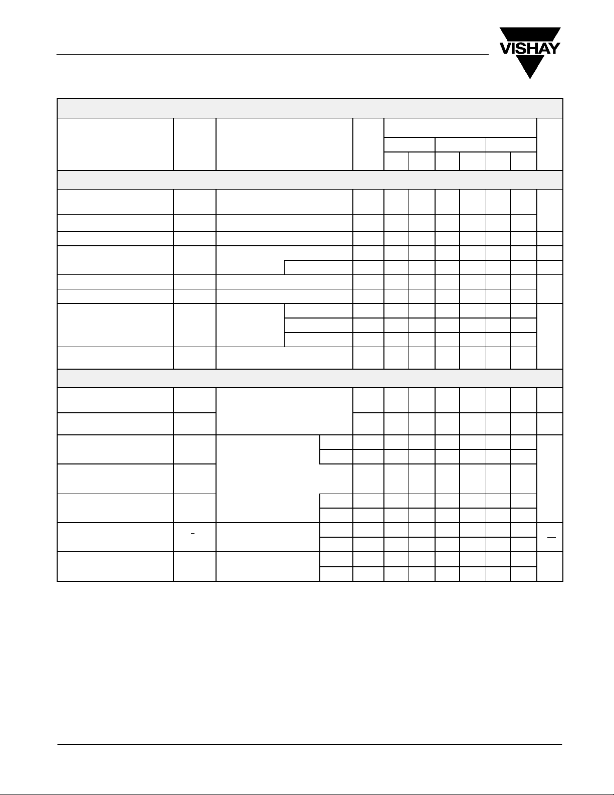
SPECIFICATIONS (T
A
= 25_C UNLESS OTHERWISE NOTED)
Limits
2N/SST5460 2N/SST5461 2N/SST5462
Parameter Symbol Test Conditions Typ
a
Min Max Min Max Min Max Unit
Static
Gate-Source
Breakdown Voltage
V
(BR)GSS
I
G
= 10 mA , V
DS
= 0 V
55 40 40 40
V
Gate-Source Cutoff Voltage V
GS(off)
V
DS
= –15 V, I
D
= –1 mA
0.75 6
1
7.5 1.8 9
V
Saturation Drain Current
b
I
DSS
V
DS
= –15 V, V
GS
= 0 V –1 –5 –2 –9 –4 –16 mA
V
GS
= 20 V, V
DS
= 0 V 0.003 5 5 5 nA
Gate Reverse Current I
GSS
T
A
= 100_C
0.0003 1 1 1
mA
Gate Operating Current I
G
V
DG
= –20 V, I
D
= –0.1 mA 3
Drain Cutoff Current I
D(off)
V
DS
= –15 V, V
GS
= 10 V –5
pA
I
D
= –0.1 mA 1.3 0.5 4
Gate-Source Voltage V
GS
V
DS
= –15 V
I
D
= –0.2 mA 2.3 0.8 4.5
I
D
= –0.4 mA 3.8 1.5 6
V
Gate-Source
Forward Voltage
V
GS(F)
I
G
= –1 mA , V
DS
= 0 V –0.7
Dynamic
Common-Source
Forward Transconductance
g
fs
V
DS
= –15 V, V
GS
= 0 V
1 4 1.5 5 2 6 mS
Common-Source
Output Conductance
g
os
V
DS
= –15 V, V
GS
= 0 V
f = 1 kHz
75 75 75
mS
Common-Source
2N 4.5 7 7 7
Reverse Transfer
Capacitance
C
iss
SST 4.5
Common-Source
Reverse Transfer
Capacitance
C
rss
V
DS
= –15 V, V
GS
= 0 V
f = 1 MHz
1.2
pF
Common-Source
2N 1.5 2 2 2
Common-Source
Output Capacitance
C
oss
SST 1.5
Equivalent Input V
DS
= –15 V, V
GS
= 0 V
2N 15 115 115 115
nV⁄
Equivalent Input
Noise Voltage
e
n
V
DS
= –15 V, V
GS
= 0 V
f = 100 Hz
SST 15
nV
⁄
√Hz
V
DS
= –15 V, V
GS
= 0 V
2N 0.2 2.5 2.5 2.5
Noise Figure NF
f = 100 Hz, R
G
= 1 M
W
BW = 1 Hz
SST 0.2
dB
Notes
a. Typical values are for DESIGN AID ONLY, not guaranteed nor subject to production testing. PSCIB
b. Pulse test: PW v300 ms duty cycle v2%.
 Loading...