


UTMC 5962-8862801VZA, 5962-8862801VYX, 5962-8862801VYC, 5962-8862801VYA, 5962-8862801VTX Datasheet
...UT1553B BCRT
FEATURES
pComprehensive MIL-STD-1553B dual-redundant Bus Controller (BC) and Remote Terminal
(RT) functions
pMIL-STD-1773 compatible
pMultiple message processing capability in BC and RT modes
pTime-tagging and message logging in RT mode
pAutomatic polling and intermessage delay in BC mode
pProgrammable interrupt scheme and internally generated interrupt history list
pRegister-oriented architecture to enhance programmability
pDMA memory interface with 64K addressability
pInternal self-test
pRemote terminal operations in ASD/ENASD-certified (SEAFAC)
pThe UT1553B BCRT is not available radiation-harden ed
pPackaged in 84-pin pingrid array, 84and 132-lead flatpack, 84-lead leadless chip carrier packages
pStandard Microcircuit Drawing 5962-88628 available - QML Q and V compliant
|
|
|
|
|
HIGH-PRIORITY |
|
REGISTERS |
||
|
|
|
|
|
|
CONTROL |
|||
|
|
|
MASTER |
STD PRIORITY LEVEL |
|
||||
|
|
|
|
|
|||||
|
12MHZ |
|
STD PRIORITY PULSE |
STATUS |
|||||
|
RESET |
|
|
||||||
|
|
|
|
|
INTERRUPT |
|
CURRENT BC BLOCK/ |
||
|
|
CLOCK & |
|
|
RT DESCRIPTOR SPACE |
||||
|
|
|
HANDLER |
|
|
|
|||
|
|
RESET |
|
|
|
|
|
POLLING COMPARE |
|
|
|
LOGIC |
|
|
|
|
|
||
|
|
|
|
|
|
|
|
||
|
|
|
|
|
|
BC PROTOCOL |
|
BUILT-IN-TEST WORD |
|
|
|
|
|
|
|
|
& MESSAGE |
|
CURRENT COMMAND |
|
|
|
SERIAL to |
|
|
HANDLER |
|
||
1553 |
|
|
PARALLEL- |
|
|
|
|
INTERRUPT LOG |
|
DATA |
DUAL |
CONVER- |
|
|
|
|
|||
|
|
|
|
LIST POINTER |
|||||
CHANNEL |
|
SION |
16 |
|
BUS |
16 |
|||
A |
CHANNEL |
|
|
|
HIGH-PRIORITY |
||||
|
ENCODER/ |
|
|
|
|
TRANSFER |
|
||
1553 |
DECODER |
PARALLEL- |
|
|
LOGIC |
|
INTERRUPT ENABLE |
||
DATA |
MODULE |
TO-SERIAL |
|
|
|
|
|
||
CHANNEL |
|
|
CONVER- |
|
|
|
16 |
HIGH-PRIORITY |
|
B |
|
|
|
SION |
|
RT PROTOCOL |
|
INTERRUPT STATUS/RESET |
|
|
|
|
|
|
|
|
|||
|
|
|
|
|
|
|
& MESSAGE |
|
16 |
|
|
|
|
|
|
|
HANDLER |
|
STANDARD INTERRUPT |
|
|
|
|
|
|
|
|
BUILT- |
ENABLE |
|
|
|
|
16 |
|
|
|
IN- |
RT ADDRESS |
TIMERON |
TIMEOUT |
|
ADDRESS |
DMA/CPU |
16 |
TEST |
|||
|
|
|
|
||||||
|
GENERATOR |
|
|
BUILT-IN-TEST |
|||||
|
|
CONTROL |
|
||||||
|
|
|
|
|
|
||||
|
|
|
|
|
|
|
|
|
START COMMAND |
|
|
|
DMA ARBITRATION |
|
|
|
|
PROGRAMMED RESET |
|
|
|
|
|
|
ADDRESS |
RT TIMER TAG |
|||
|
|
|
REGISTER CONTROL |
|
|||||
|
|
|
|
|
|
RESET COMMAND |
|||
|
|
DUAL-PORT MEMORY CONTROL |
|
|
|
||||
|
|
|
|
|
|
||||
|
|
|
|
|
|
|
|
|
16 |
|
|
|
|
|
|
|
|
|
16 |
|
|
|
|
|
|
|
|
|
DATA |
Figure 1. BCRT Block Diagram
BCRT-1

Table of Contents
1.0 INTRODUCTION . . . . . . . . . . . . . . . . . . . . . . . . . . . . . . . . . . . . . . . . . . . . . . . . . . . . . . . . . . . . 3
1.1 Features - Remote Terminal (RT) Mode . . . . . . . . . . . . . . . . . . . . . . . . . . . . . . .3
1.2 Features - Bus Controller (BC) Mode. . . . . . . . . . . . . . . . . . . . . . . . . . . . . . . . .3
2.0 PIN IDENTIFICATION AND DESCRIPTION . . . . . . . . . . . . . . . . . . . . . . . . . . . . . . . . . . . . 4
3.0 INTERNAL REGISTERS . . . . . . . . . . . . . . . . . . . . . . . . . . . . . . . . . . . . . . . . . . . . . . . . . . . . |
12 |
4.0 SYSTEM OVERVIEW . . . . . . . . . . . . . . . . . . . . . . . . . . . . . . . . . . . . . . . . . . . . . . . . . . . . . . . 18
5.0 SYSTEM INTERFACE. . . . . . . . . . . . . . . . . . . . . . . . . . . . . . . . . . . . . . . . . . . . . . . . . . . . . . . 19
5.1 DMA Transfers . . . . . . . . . . . . . . . . . . . . . . . . . . . . . . . . . . . . . . . . . . . . . . . . .19
5.2 Hardware Interface . . . . . . . . . . . . . . . . . . . . . . . . . . . . . . . . . . . . . . . . . . . . . .19
5.3 CPU Interconnection . . . . . . . . . . . . . . . . . . . . . . . . . . . . . . . . . . . . . . . . . . . . .19
5.4 RAM Interface . . . . . . . . . . . . . . . . . . . . . . . . . . . . . . . . . . . . . . . . . . . . . . . . .20
5.5 Transmitter/Receiver Interface . . . . . . . . . . . . . . . . . . . . . . . . . . . . . . . . . . . . .20
6.0 REMOTE TERMINAL ARCHITECTURE . . . . . . . . . . . . . . . . . . . . . . . . . . . . . . . . . . . . . . 21
6.1 RT Functional Operation . . . . . . . . . . . . . . . . . . . . . . . . . . . . . . . . . . . . . . . . . .22
6.1.1 RT Subaddress Descriptor Definitions . . . . . . . . . . . . . . . . . . . . . . . . . .22
6.1.2 Message Status Word. . . . . . . . . . . . . . . . . . . . . . . . . . . . . . . . . . . . . . .24
6.1.3 Mode Code Descriptor Definition . . . . . . . . . . . . . . . . . . . . . . . . . . . . .25
6.2 RT Error Detection . . . . . . . . . . . . . . . . . . . . . . . . . . . . . . . . . . . . . . . . . . . . . .27
6.3 RT Operational Sequence . . . . . . . . . . . . . . . . . . . . . . . . . . . . . . . . . . . . . . . . .27
7.0 BUS CONTROLLER ARCHITECTURE . . . . . . . . . . . . . . . . . . . . . . . . . . . . . . . . . . . . . . . |
28 |
7.1 BC Functional Operation . . . . . . . . . . . . . . . . . . . . . . . . . . . . . . . . . . . . . . . . .29
7.2 Polling . . . . . . . . . . . . . . . . . . . . . . . . . . . . . . . . . . . . . . . . . . . . . . . . . . . . . . . .31
7.3 BC Error Detection . . . . . . . . . . . . . . . . . . . . . . . . . . . . . . . . . . . . . . . . . . . . . .31
7.4 BC Operational Sequence . . . . . . . . . . . . . . . . . . . . . . . . . . . . . . . . . . . . . . . . .31
7.5 BC Operational Example . . . . . . . . . . . . . . . . . . . . . . . . . . . . . . . . . . . . . . . . .33
8.0 EXCEPTION HANDLING AND INTERRUPT LOGGING . . . . . . . . . . . . . . . . . . . . . . . . 34
9.0 MAXIMUM AND RECOMMENDED OPERATING CONDITIONS . . . . . . . . . . . . . . . . 37
10.0 DC ELECTRICAL CHARACTERISTICS . . . . . . . . . . . . . . . . . . . . . . . . . . . . . . . . . . . . . . 38
11.0 AC ELECTRICAL CHARACTERISTICS . . . . . . . . . . . . . . . . . . . . . . . . . . . . . . . . . . . . . . 39
12.0 PACKAGE OUTLINE DRAWINGS . . . . . . . . . . . . . . . . . . . . . . . . . . . . . . . . . . . . . . . . . . . . 46
BCRT-2

1.0 INTRODUCTION
The monolithic CMOS UT1553B BCRT provides the system designer with an intelligent solution to MIL-STD-1553B multiplexed serial data bus design problems. The UT1553B BCRT is a single-chip device that implements two of the defined MIL-STD-1553B functions - Bus Controller and Remote Terminal. Designed to reduce host CPU overhead, the BCRT’s powerful state machines automatically execute message transfers, provide interrupts, and generate status information. Multiple registers offer many programmable functions as well as extensive information for host use. In the BC mode, the BCRT uses a linked-list message scheme to provide the host with message chaining capability. The BCRT enhances memory use by supporting variable-size, relocatable data blocks. In the RT mode, the BCRT implements time-tagging and message history functions. It also supports multiple (up to 128) message buffering and variable length messages to any subaddress.
The UT1553B BCRT is an intelligent, versatile, and easy to implement device -- a powerful asset to system designers.
1.1 Features - Remote Terminal (RT) Mode
Indexing
The BCRT is programmable to index or buffer messages on a subaddress-by-subaddress basis. The BCRT, which can index as many as 128 messages, can also assert an interrupt when either the selected number of messages is reached or every time a specified subaddress is accessed.
Variable Space Allocation
The BCRT can use as little or as much memory (up to 64K) as needed.
Selectable Data Storage
Address programmability within the BCRT provides flexible data placement and convenient access.
Sequential Data Storage
The BCRT stores/retrieves, by subaddress, all messages in the order in which they are transacted.
Sequential Message Status Information
The BCRT provides message validity, time-tag, and wordcount information, and stores it sequentially in a separate, cross-referenced list.
Illegalizing Mode Codes and Subaddresses
The host can declare mode codes and subaddresses illegal by setting the appropriate bit(s) in memory.
Programmable Interrupt Selection
The host CPU can select various events to cause an interrupt with provision for high and standard priority interrupts.
Interrupt History List
The BCRT provides an Interrupt History List that records, in the order of occurrence, the events that caused the interrupts. The list length is programmable.
1.2 Features - Bus Controller (BC) Mode
Multiple Message Processing
The BCRT autonomously processes any number of messages or lists of messages that may be stored in a 64K memory space.
Automatic Intermessage Delay
When programmed by the host, the BCRT can delay a host-specified time before executing the next message in sequence.
Automatic Polling
When polling, the BCRT interrogates the remote terminals and then compares their status word responses to the contents of the Polling Compare
Register. The BCRT can interrupt the host CPU if an erroneous remote terminal status word response occurs.
Automatic Retry
The BCRT can automatically retry a message on busy, message error, and/or response time-out conditions. The BCRT can retry up to four times on the same or on the alternate bus.
Programmable Interrupt Selection
The host CPU can select various events to cause an interrupt with provision for high and standard priority interrupts.
Interrupt History List
The BCRT provides an Interrupt History List that records, in the order of occurrence, the events that caused the interrupts. The list length is programmable.
Variable Space Allocation
The BCRT uses as little or as much memory (up to 64K) as needed.
Selectable Data Storage
Address programmability within the BCRT provides flexible data placement and convenient access.
BCRT-3

2.0 PIN IDENTIFICATION AND DESCRIPTION
|
|
|
|
|
|
TAZ |
|
13 |
(K3) |
|
||||
|
|
|
|
|||||||||||
BIPHASE OUT |
|
|
|
|
|
TAO |
|
14 |
(L2) |
|
||||
|
|
|
||||||||||||
|
|
|
|
|
TBZ |
|
17 |
(L4) |
|
|||||
|
|
|
|
|
|
|
|
|||||||
|
|
|
|
|
|
TBO |
|
18 |
(K6) |
|
||||
|
|
|
|
|||||||||||
|
|
|
|
|
|
RAZ |
|
15 |
(L3) |
|
||||
|
|
|
|
|||||||||||
BIPHASE IN |
|
|
|
|
|
RAO |
|
16 |
(K4) |
|
||||
|
|
|
||||||||||||
|
|
|
|
|
RBZ |
|
19 |
(K5) |
|
|||||
|
|
|
||||||||||||
|
|
|
|
|
|
RBO |
|
20 |
(L5) |
|
||||
|
|
|
|
|||||||||||
|
|
|
|
|
|
RTA0 |
|
28 |
(K8) |
|
||||
|
|
|
|
|||||||||||
|
|
|
|
|
|
RTA1 |
|
29 |
(L9) |
|
||||
|
|
|
|
|||||||||||
TERMINAL |
|
|
|
|
|
RTA2 |
|
30 |
(L10) |
|||||
|
|
|||||||||||||
ADDRESS* * |
|
|
|
|
|
RTA3 |
|
31 |
(K9) |
|
||||
|
|
|
||||||||||||
|
|
|
|
|
|
RTA4 |
|
32 |
(L11) |
|||||
|
|
|
||||||||||||
|
|
|
|
|
RTPTY |
|
33 |
(K10) |
||||||
|
|
|
||||||||||||
|
|
|
|
|
|
|
|
|
|
|
|
|
|
|
|
|
|
STDINTL |
|
68 |
(A6) + |
||||||||
|
|
|
||||||||||||
|
|
|
STDINTP |
|
69 |
(A4) |
|
|||||||
|
|
|
|
|||||||||||
|
|
|
|
|
|
HPINT |
|
|
70 |
(B4) + |
||||
|
|
|
||||||||||||
STATUS |
|
TIMERON |
|
25 |
(K7) |
|
||||||||
|
|
|
||||||||||||
|
|
COMSTR |
|
27 |
(L8) |
|
||||||||
|
|
|
||||||||||||
SIGNALS |
|
|
|
|
SSYSF |
|
72 |
(A2) |
|
|||||
|
|
|||||||||||||
|
|
|
||||||||||||
|
|
|
|
|
BCRTF |
|
75 |
(B2) |
|
|||||
|
|
|
|
|||||||||||
|
|
|
|
|
CHA/B |
|
26 |
(J7) |
|
|||||
|
|
|
|
|||||||||||
|
|
|
|
|
|
TEST |
|
73 |
(B3)* |
|||||
|
|
|
||||||||||||
|
|
|
|
|
|
|
|
|
|
|
|
|
|
|
|
|
|
|
|
DMAR |
|
56 |
(A10) + |
||||||
|
|
|
||||||||||||
|
|
|
|
|
DMAG |
|
|
|
57 |
(A9) |
|
|||
|
|
|
|
|||||||||||
|
|
|
|
|
DMAGO |
|
|
|||||||
DMA |
|
|
|
|
|
67 |
(B5) |
|
||||||
|
|
|
||||||||||||
SIGNALS |
|
|
|
|
DMACK |
|
58 |
(B8) |
+ |
|||||
|
|
|
|
|
BURST |
|
74 |
(A1) |
|
|||||
|
|
|
|
|||||||||||
|
|
|
|
|
TSCTL |
|
55 |
(B9) |
|
|||||
|
|
|
|
|||||||||||
|
|
|
|
|
|
|
|
|
|
|
61 |
(B7) |
|
|
|
|
|
|
|
|
|
RD |
|
|
|
||||
|
|
|
|
|
|
WR |
|
60 |
(C7) |
|
||||
|
|
|
|
|||||||||||
|
|
|
|
|
|
|
|
CS |
|
62 |
(A7) |
|
||
|
|
|
|
|||||||||||
|
|
|
|
|
|
AEN |
|
66 |
(A5) |
|
||||
|
|
|
|
|||||||||||
|
|
BCRTSEL |
|
11 |
(L1) * * |
|||||||||
|
|
|
||||||||||||
CONTROL |
|
|
|
|
|
LOCK |
|
12 |
(K2) |
* * |
||||
|
|
|||||||||||||
SIGNALS |
|
|
|
|
|
MRST |
|
|
10 |
(J2) |
|
|||
|
|
|
|
EXTOVR |
|
24 |
(L7) * * |
|||||||
|
|
|
||||||||||||
|
|
|
|
|
|
RRD |
|
53 |
(A11) |
|||||
|
|
|
||||||||||||
|
|
|
|
|
|
RWR |
|
|
52 |
(C10) |
||||
|
|
|
||||||||||||
|
|
|
|
|
MEMCSI |
|
59 |
(A8) * * |
||||||
|
|
|
||||||||||||
|
|
|
MEMCSO |
|
54 |
(B10) |
||||||||
|
|
|
||||||||||||
|
|
|
|
|
|
|
|
|
|
|
|
|
|
|
(J10) |
34 |
|
A0 ++ |
|
|
(K11) |
35 |
|
A1 ++ |
|
|
|
|
|
|||
(J11) |
36 |
|
A2 ++ |
|
|
|
|
|
|||
(H10) |
37 |
|
A3 ++ |
|
|
|
|
|
|||
(H11) |
38 |
|
A4 |
|
|
|
|
|
|||
(G9) |
39 |
|
A5 |
|
|
|
|
|
|||
(G10) |
40 |
|
A6 |
|
|
|
|
|
|||
(G11) |
41 |
|
A7 |
|
ADDRESS+ |
|
|
||||
(E9) |
44 |
|
A8 |
|
LINES |
|
|
||||
(E11) |
45 |
|
A9 |
|
|
|
|
|
|||
(E10) |
46 |
|
A10 |
|
|
|
|
|
|||
(F11) |
47 |
|
A11 |
|
|
|
|
|
|||
(D11) |
48 |
|
A12 |
|
|
|
|
|
|||
(D10) |
49 |
|
A13 |
|
|
|
|
|
|||
(C11) |
50 |
|
A14 |
|
|
|
|
|
|||
(B11) |
51 |
|
A15 |
|
|
|
|
|
|||
(K1) |
9 |
|
D0 |
|
|
|
|
|
|||
(J1) |
8 |
|
D1 |
|
|
|
|
|
|||
(H2) |
7 |
|
D2 |
|
|
|
|
|
|||
(H1) |
6 |
|
D3 |
|
|
|
|
|
|||
(G3) |
5 |
|
D4 |
|
|
|
|
|
|||
(G2) |
4 |
|
D5 |
|
|
|
|
|
|||
(G1) |
3 |
|
D6 |
|
|
|
|
|
|||
(F1) |
2 |
|
D7 |
|
DATA |
|
|
||||
(E1) |
83 |
|
D8 |
|
LINES++ |
|
|
||||
(E2) |
82 |
|
D9 |
|
|
|
|
|
|||
(F2) |
81 |
|
D10 |
|
|
|
|
|
|||
(D1) |
80 |
|
D11 |
|
|
|
|
|
|||
(D2) |
79 |
|
D12 |
|
|
|
|
|
|||
(C1) |
78 |
|
D13 |
|
|
|
|
|
|||
(B1) |
77 |
|
D14 |
|
|
|
|
|
|||
(C2) |
76 |
|
D15 |
|
|
|
|
|
|||
(L6) |
23 |
|
VDD |
|
|
|
|
|
|||
(F9) |
43 |
|
VDD |
|
POWER |
|
|
||||
(C6) |
64 |
|
VDD |
|
|
|
|
|
|||
(E3) |
84 |
|
VDD |
|
|
|
|
|
|||
(F3) |
1 |
|
VSS |
|
|
(J6) |
22 |
|
VSS |
|
GROUND |
|
|
||||
(F10) |
42 |
|
VSS |
|
|
|
|
||||
(B6) |
63 |
|
VSS |
|
|
|
|
|
|||
(J5) |
21 |
|
CLK |
|
|
|
|
|
|||
(C5) |
65 |
|
MCLK |
|
CLOCK |
|
|
||||
(A3) |
71 |
|
MCLKD2 |
|
SIGNALS |
|
|
||||
|
|
|
|
|
|
**Pin internally pulled up.
+ Pin at high impedance when not asseted
++Bidirectional pin.
*Formerly MEMWIN.
( ) Pingrid arraylead identification in parentheses. LCC, flatpack pin number not in parentheses.
Figure 2a. BCRT 84-lead Functional Pin Description
BCRT-4
|
|
|
|
|
|
|
TAZ |
|
3 |
|||
|
|
|
||||||||||
BIPHASE OUT |
|
|
|
|
|
|
TAO |
|
4 |
|||
|
|
|||||||||||
|
|
|
|
|
|
TBZ |
|
10 |
||||
|
|
|
|
|
|
|
|
|||||
|
|
|
|
|
|
|
TBO |
|
11 |
|||
|
|
|
||||||||||
|
|
|
|
|
|
|
RAZ |
|
7 |
|||
|
|
|
||||||||||
BIPHASE IN |
|
|
|
|
|
|
RAO |
|
9 |
|||
|
|
|||||||||||
|
|
|
|
|
|
RBZ |
|
13 |
||||
|
|
|||||||||||
|
|
|
|
|
|
|
RBO |
|
15 |
|||
|
|
|
||||||||||
|
|
|
|
|
|
|
RTA0 |
|
27 |
|||
|
|
|
||||||||||
|
|
|
|
|
|
|
RTA1 |
|
29 |
|||
|
|
|
||||||||||
TERMINAL |
|
|
|
|
|
|
RTA2 |
|
30 |
|||
|
|
|||||||||||
ADDRESS* * |
|
|
|
|
|
|
RTA3 |
|
31 |
|||
|
|
|||||||||||
|
|
|
|
|
|
|
RTA4 |
|
32 |
|||
|
|
|
||||||||||
|
|
|
|
|
|
RTPTY |
|
35 |
||||
|
|
|
||||||||||
|
|
|
|
|
|
|
|
|
|
|
|
|
|
|
|
|
|
|
STDINT |
|
89 |
||||
|
|
|
||||||||||
|
|
|
|
STDPUL |
|
90 |
||||||
|
|
|
||||||||||
|
|
|
|
|
|
|
HPINT |
|
|
92 |
||
|
|
|
||||||||||
STATUS |
|
TIMERON |
|
22 |
||||||||
|
|
|||||||||||
|
|
COMSTR |
|
27 |
||||||||
|
|
|||||||||||
SIGNALS |
|
|
|
|
|
SSYSF |
|
95 |
||||
|
||||||||||||
|
|
|||||||||||
|
|
|
|
|
|
BCRTF |
|
101 |
||||
|
|
|
||||||||||
|
|
|
|
|
|
CHA/B |
|
24 |
||||
|
|
|
||||||||||
|
|
|
|
|
|
|
TEST |
|
97 * |
|||
|
|
|
||||||||||
|
|
|
|
|
|
|
|
|
|
|
|
|
|
|
|
|
|
|
|
DMAR |
|
70 |
|||
|
|
|
||||||||||
|
|
|
|
|
|
DMAG |
|
|
|
72 |
||
|
|
|
||||||||||
|
|
|
|
DMAGO |
|
|||||||
DMA |
|
|
|
|
88 |
|||||||
|
|
|||||||||||
SIGNALS |
|
|
|
|
DMACK |
|
74 |
|||||
|
|
|
|
|
|
BURST |
|
98 |
||||
|
|
|
||||||||||
|
|
|
|
|
|
TSCTL |
|
69 |
||||
|
|
|
||||||||||
|
|
|
|
|
|
|
|
|
|
|
79 |
|
|
|
|
|
|
|
|
RD |
|
||||
|
|
|
||||||||||
|
|
|
|
|
|
|
WR |
|
77 |
|||
|
|
|
||||||||||
|
|
|
|
|
|
|
|
CS |
|
81 |
||
|
|
|
||||||||||
|
|
|
|
|
|
|
AEN |
|
86 |
|||
|
|
|
||||||||||
|
|
BCRTSEL |
|
131 |
||||||||
|
|
|
||||||||||
CONTROL |
|
|
|
|
|
|
LOCK |
|
2 |
|||
|
|
|||||||||||
SIGNALS |
|
|
|
|
|
|
MRST |
|
|
130 |
||
|
|
|
|
EXTOVR |
|
20 |
||||||
|
|
|
||||||||||
|
|
|
|
|
|
|
RRD |
|
65 |
|||
|
|
|
||||||||||
|
|
|
|
|
|
|
RWR |
|
|
64 |
||
|
|
|
||||||||||
|
|
|
|
MEMCSI |
|
|||||||
|
|
|
|
|
75 |
|||||||
|
|
|
||||||||||
|
|
|
MEMCSO |
|
68 |
|||||||
|
|
|
||||||||||
**Pin internally pulled up.
+ Pin at high impedance when not asseted
++Bidirectional pin.
*Formerly MEMWIN.
36 |
|
A0 ++ |
|
|
|
|
|
||
37 |
|
A1 ++ |
|
|
|
|
|
||
40 |
|
A2 ++ |
|
|
|
|
|
||
41 |
|
A3 ++ |
|
|
|
|
|
||
42 |
|
A4 |
|
|
|
|
|
||
45 |
|
A5 |
|
|
|
|
|
||
47 |
|
A6 |
|
ADDRESS+ |
|
|
|||
51 |
|
A7 |
|
|
|
|
|||
52 |
|
A8 |
|
LINES |
|
|
|||
54 |
|
A9 |
|
|
|
|
|
56 A10
A10
57 A11
A11
58 A12
A12
60 A13
A13
61 A14
A14
63  A15
A15
129 |
|
|
|
|
|
D0 |
|
|
|
|
|
||||
|
|
|
|
|
|
|
|
|
|||||||
127 |
|
|
|
|
|
D1 |
|
|
|
|
|
||||
|
|
|
|
|
|
|
|
|
|||||||
125 |
|
|
|
|
|
D2 |
|
|
|
|
|
||||
|
|
|
|
|
|
|
|
|
|||||||
124 |
|
|
|
|
|
D3 |
|
|
|
|
|
||||
|
|
|
|
|
|
|
|
|
|||||||
122 |
|
|
|
|
|
D4 |
|
|
|
|
|
||||
|
|
|
|
|
|
|
|
|
|||||||
120 |
|
|
|
|
|
D5 |
|
|
|
|
|
||||
|
|
|
|
|
|
|
|
|
|||||||
119 |
|
|
|
|
|
|
D6 |
|
|
|
|
|
|||
|
|
|
|
|
|
|
|
|
|||||||
118 |
|
|
|
|
|
|
D7 |
|
|
|
|
DATA |
|||
114 |
|
|
|
|
|
|
D8 |
|
|
|
LINES++ |
||||
|
|
|
|
|
|||||||||||
112 |
|
|
|
|
|
|
D9 |
|
|
|
|
||||
|
|
|
|
|
|
|
|
||||||||
110 |
|
|
|
|
|
|
D10 |
|
|
|
|
||||
|
|
|
|
|
|
|
|
||||||||
108 |
|
|
|
|
|
D11 |
|
|
|
|
|||||
|
|
|
|
|
|
|
|
||||||||
107 |
|
|
|
|
|
D12 |
|
|
|
|
|||||
|
|
|
|
|
|
|
|
||||||||
105 |
|
|
|
|
|
D13 |
|
|
|
|
|||||
|
|
|
|
|
|
|
|
||||||||
103 |
|
|
|
|
|
D14 |
|
|
|
|
|||||
|
|
|
|
|
|
|
|
||||||||
102 |
|
|
|
|
|
D15 |
|
|
|
|
|||||
|
|
|
|
|
|
|
|
||||||||
17 |
|
|
|
|
|
|
|
|
VDD |
|
|
|
|
||
|
|
|
|
|
|
|
|
|
|
|
|
||||
34 |
|
|
|
|
|
|
|
|
VDD |
|
|
|
|
||
|
|
|
|
|
|
|
|
|
|||||||
50 |
|
|
|
|
|
|
|
|
VDD |
|
|
|
POWER |
||
|
|
|
|
|
|
|
|
||||||||
66 |
|
|
|
|
|
|
|
|
VDD |
|
|
|
|||
|
|
|
|
|
|
|
|
|
|
|
|
||||
83 |
|
|
|
|
|
|
|
|
VDD |
|
|
|
|
||
|
|
|
|
|
|
|
|
|
|||||||
100 |
|
|
|
|
VDD |
|
|
|
|
|
|||||
115 |
|
|
|
|
VDD |
|
|
|
|
|
|||||
|
|
|
|
|
|
|
|
||||||||
132 |
|
|
|
|
VDD |
|
|
|
|
|
|||||
|
|
|
|
|
|
|
|
||||||||
1 |
|
|
|
|
|
|
|
|
VSS |
|
|
|
|
||
|
|
|
|
|
|
|
|
|
|
||||||
16 |
|
|
|
|
|
|
|
|
VSS |
|
|
|
|
||
|
|
|
|
|
|
|
|
|
|
|
|
||||
|
|
|
|
|
|
|
|
|
|
||||||
33 |
|
|
|
|
|
|
|
|
VSS |
|
|
|
|
||
|
|
|
|
|
|
|
|
|
|
||||||
49 |
|
|
|
|
|
|
|
|
VSS |
|
|
|
GROUND |
||
|
|
|
|
|
|
|
|
|
|
|
|||||
67 |
|
|
|
|
|
|
|
|
VSS |
|
|
|
|||
|
|
|
|
|
|
|
|
||||||||
82 |
|
|
|
|
|
|
|
|
VSS |
|
|
|
|
||
|
|
|
|
|
|
|
|
|
|
||||||
99 |
|
|
|
|
|
|
|
|
VSS |
|
|
|
|
||
|
|
|
|
|
|
|
|
|
|
|
|||||
116 |
|
|
|
|
|
|
|
|
VSS |
|
|
|
|
||
|
|
|
|
|
|
|
|
|
|
|
|
||||
18 |
|
|
|
|
|
|
|
|
CLK |
|
|
|
|
||
|
|
|
|
|
|
|
|
|
|
||||||
85 |
|
|
|
|
|
|
|
|
MCLK |
|
|
|
CLOCK |
||
|
|
|
|
|
|
|
|||||||||
94 |
|
|
|
|
|
|
|
|
MCKD2 |
|
|
|
SIGNALS |
||
|
|
|
|
|
|||||||||||
( ) Pingrid arraylead identification in parentheses. LCC, flatpack pin number not in parentheses.
Figure 2b. BCRT 132-lead Functional Pin Description
BCRT-5

Legend for TYPE and ACTIVE fields:
TUI = TTL input (pull-up)
AL = Active low
AH = Active high
ZL = Active low - inactive state is high impedance
TI = TTL input
TO = TTL output
TTO = Three-state TTL output
TTB = Bidirectional
Notes:
1.Address and data buses are in the high-impedance state when idle.
2.Flatpack pin numbers are same as LCC.
ADDRESS BUS
NAME |
|
PIN NUMBER |
|
TYPE |
ACTIVE |
DESCRIPTION |
|
LCC/FP |
PGA |
132 FP |
|
|
|
AO |
34 |
J10 |
36 |
TTB |
-- |
Bit 0 (LSB) of the Address Bus |
A1 |
35 |
K11 |
37 |
TTB |
-- |
Bit 1 of the Address Bus |
A2 |
36 |
J11 |
40 |
TTB |
-- |
Bit 2 of the Address Bus |
A3 |
37 |
H10 |
41 |
TTB |
-- |
Bit 3 of the Address Bus |
A4 |
38 |
H11 |
42 |
TTO |
-- |
Bit 4 of the Address Bus |
A5 |
39 |
G9 |
45 |
TTO |
-- |
Bit 5 of the Address Bus |
A6 |
40 |
G10 |
47 |
TTO |
-- |
Bit 6 of the Address Bus |
A7 |
41 |
G11 |
51 |
TTO |
-- |
Bit 7 of the Address Bus |
A8 |
44 |
E9 |
52 |
TTO |
-- |
Bit 8 of the Address Bus |
A9 |
45 |
E11 |
54 |
TTO |
-- |
Bit 9 of the Address Bus |
A10 |
46 |
E10 |
56 |
TTO |
-- |
Bit 10 of the Address Bus |
A11 |
47 |
F11 |
57 |
TTO |
-- |
Bit 11 of the Address Bus |
A12 |
48 |
D11 |
58 |
TTO |
-- |
Bit 12 of the Address Bus |
A13 |
49 |
D10 |
60 |
TTO |
-- |
Bit 13 of the Address Bus |
A14 |
50 |
C11 |
61 |
TTO |
-- |
Bit 14 of the Address Bus |
A15 |
51 |
B11 |
63 |
TTO |
-- |
Bit 15 (MSB) of the Address Bus |
BCRT-6

DATA BUS |
|
|
|
|
|
|
NAME |
|
PIN NUMBER |
|
TYPE |
ACTIVE |
DESCRIPTION |
|
LCC/FP |
PGA |
132 FP |
|
|
|
DO |
9 |
KA |
129 |
TTB |
-- |
Bit 0 (LSB) of the Data Bus |
D1 |
8 |
J1 |
127 |
TTB |
-- |
Bit 1 of the Data Bus |
D2 |
7 |
H2 |
125 |
TTB |
-- |
Bit 2 of the Data Bus |
D3 |
6 |
H1 |
124 |
TTB |
-- |
Bit 3 of the Data Bus |
D4 |
5 |
G3 |
122 |
TTB |
-- |
Bit 4 of the Data Bus |
D5 |
4 |
G2 |
120 |
TTB |
-- |
Bit 5 of the Data Bus |
D6 |
3 |
G1 |
119 |
TTB |
-- |
Bit 6 of the Data Bus |
D7 |
2 |
F1 |
118 |
TTB |
-- |
Bit 7 of the Data Bus |
D8 |
83 |
E1 |
114 |
TTB |
-- |
Bit 8 of the Data Bus |
D9 |
82 |
E2 |
112 |
TTB |
-- |
Bit 9 of the Data Bus |
D10 |
81 |
F2 |
110 |
TTB |
-- |
Bit 10 of the Data Bus |
D11 |
80 |
D1 |
108 |
TTB |
-- |
Bit 11 of the Data Bus |
D12 |
79 |
D2 |
107 |
TTB |
-- |
Bit 12 of the Data Bus |
D13 |
78 |
C1 |
105 |
TTB |
-- |
Bit 13 of the Data Bus |
D14 |
77 |
B1 |
103 |
TTB |
-- |
Bit 14 of the Data Bus |
D15 |
76 |
C2 |
102 |
TTB |
-- |
Bit 15 (msb) of the Data Bus |
TERMINAL ADDRESS INPUTS |
|
|
|
|
||
NAME |
|
PIN NUMBER |
|
TYPE |
ACTIVE |
DESCRIPTION |
||
|
LCC/FP |
|
PGA |
|
132 FP |
|
|
|
RTA0 |
28 |
|
K8 |
|
27 |
TUI |
-- |
Remote Terminal Address Bit 0 |
|
|
|
|
|
|
|
|
(LSB). The entire RT address is |
|
|
|
|
|
|
|
|
strobed in at Master Reset. Verify |
|
|
|
|
|
|
|
|
it by reading the Remote |
|
|
|
|
|
|
|
|
Terminal Address Register. All |
|
|
|
|
|
|
|
|
the Remote Terminal Address |
|
|
|
|
|
|
|
|
bits are internally pulled up. |
RTA1 |
29 |
|
L9 |
|
29 |
TUI |
-- |
Remote Terminal Address Bit |
|
|
|
|
|
|
|
|
1. This is bit 1 of the Remote |
|
|
|
|
|
|
|
|
Terminal Address. |
RTA2 |
30 |
|
L10 |
|
30 |
TUI |
-- |
Remote Terminal Address Bit |
|
|
|
|
|
|
|
|
2. This is bit 2 of the Remote |
|
|
|
|
|
|
|
|
Terminal Address. |
RTA3 |
31 |
|
K9 |
|
31 |
TUI |
-- |
Remote Terminal Address Bit |
|
|
|
|
|
|
|
|
3. This is bit 3 of the Remote |
|
|
|
|
|
|
|
|
Terminal Address. |
RTA4 |
32 |
|
L11 |
|
32 |
TUI |
-- |
Remote Terminal Address Bit |
|
|
|
|
|
|
|
|
4. This is bit 4 (MSB) of the |
|
|
|
|
|
|
|
|
Remote Terminal Address. |
RTA5 |
33 |
|
K10 |
|
35 |
TUI |
-- |
Remote Terminal (Address) |
|
|
|
|
|
|
|
|
Parity. This is oddof the |
|
|
|
|
|
|
|
|
Remote Terminal Address. |
BCRT-7

|
|
CONTROL SIGNALS |
|
|
|
|
|
|
|
|
|
|
|
|
|
||||||||||||
|
|
|
|
|
|
|
|
|
|
|
|
|
|||||||||||||||
|
|
NAME |
|
PIN NUMBER |
|
TYPE |
ACTIVE |
|
|
|
|
DESCRIPTION |
|||||||||||||||
|
|
|
|
|
|
|
|
|
|
|
|
|
|
LCC/FP |
|
PGA |
|
132 FP |
|
|
|
|
|
|
|
|
|
|
|
|
|
|
RD |
|
|
|
|
|
|
|
61 |
|
B7 |
|
79 |
TI |
AL |
Read. The host uses this in conjunction |
|||||||
|
|
|
|
|
|
|
|
|
|
|
|
|
|
|
|
|
|
|
|
|
with |
CS |
to read an internal BCRT register. |
||||
|
|
|
|
|
|
|
|
|
|
|
|
|
|
|
|
|
|
|
|
||||||||
|
|
|
|
|
WR |
|
|
|
|
|
|
60 |
|
C7 |
|
77 |
TI |
AL |
Write. The host uses this in conjunction |
||||||||
|
|
|
|
|
|
|
|
|
|
|
|
|
|
|
|
|
|
|
|
|
with CS to write an internal BCRT |
||||||
|
|
|
|
|
|
|
|
|
|
|
|
|
|
|
|
|
|
|
|
|
register. |
||||||
|
|
|
|
|
|
|
|
|
|
|
|
|
|
|
|
|
|
|
|
|
|||||||
|
|
|
|
|
|
CS |
|
|
|
|
|
|
|
62 |
|
A7 |
|
81 |
TI |
AL |
Chip Select. This selects theBCRT when |
||||||
|
|
|
|
|
|
|
|
|
|
|
|
|
|
|
|
|
|
|
|
|
accessing the BCRT’s internal register. |
||||||
|
|
|
|
AEN |
66 |
|
A5 |
|
86 |
TI |
AH |
Address Enable. The hostCPU uses AEN |
|||||||||||||||
|
|
|
|
|
|
|
|
|
|
|
|
|
|
|
|
|
|
|
|
|
to indicate to the BCRT that the BCRT’s |
||||||
|
|
|
|
|
|
|
|
|
|
|
|
|
|
|
|
|
|
|
|
|
addresslines can be asserted; this is a |
||||||
|
|
|
|
|
|
|
|
|
|
|
|
|
|
|
|
|
|
|
|
|
precautionary signal provided to avoid |
||||||
|
|
|
|
|
|
|
|
|
|
|
|
|
|
|
|
|
|
|
|
|
address bus crash. If not used, it must be |
||||||
|
|
|
|
|
|
|
|
|
|
|
|
|
|
|
|
|
|
|
|
|
tied high. |
||||||
BCRTSEL |
11 |
|
L1 |
|
131 |
TUI |
-- |
|
|
|
Select. This selects between |
||||||||||||||||
BC/RT |
|||||||||||||||||||||||||||
|
|
|
|
|
|
|
|
|
|
|
|
|
|
|
|
|
|
|
|
|
either the Bus Controller or Remote Ter- |
||||||
|
|
|
|
|
|
|
|
|
|
|
|
|
|
|
|
|
|
|
|
|
minal mode. The BC/RT Mode Select bit |
||||||
|
|
|
|
|
|
|
|
|
|
|
|
|
|
|
|
|
|
|
|
|
in the Control Register overrides this |
||||||
|
|
|
|
|
|
|
|
|
|
|
|
|
|
|
|
|
|
|
|
|
input if the Lock pin is not high. This pin |
||||||
|
|
|
|
|
|
|
|
|
|
|
|
|
|
|
|
|
|
|
|
|
is internally pulled high. |
||||||
|
|
|
|
|
|
|
|
|
|
|
|
||||||||||||||||
|
|
|
LOCK |
12 |
|
K2 |
|
2 |
TUI |
AH |
Lock. When set, this pin prevents inter- |
||||||||||||||||
|
|
|
|
|
|
|
|
|
|
|
|
|
|
|
|
|
|
|
|
|
nal changes to both the RT address and |
||||||
|
|
|
|
|
|
|
|
|
|
|
|
|
|
|
|
|
|
|
|
|
BC/RT mode select functions. This pin is |
||||||
|
|
|
|
|
|
|
|
|
|
|
|
|
|
|
|
|
|
|
|
|
internally pulled high. |
||||||
|
|
|
|
|
|
|
|
|
|
|
|
|
|||||||||||||||
|
|
EXTOVR |
|
|
24 |
|
L7 |
|
20 |
TUI |
AL |
External Override. Use this in multi- |
|||||||||||||||
|
|
|
|
|
|
|
|
|
|
|
|
|
|
|
|
|
|
|
|
|
redundant applications. Upon receipt, the |
||||||
|
|
|
|
|
|
|
|
|
|
|
|
|
|
|
|
|
|
|
|
|
BCRT aborts all current activity. |
||||||
|
|
|
|
|
|
|
|
|
|
|
|
|
|
|
|
|
|
|
|
|
EXTOVR should be connected to |
COM- |
|
||||
|
|
|
|
|
|
|
|
|
|
|
|
|
|
|
|
|
|
|
|
|
STR output of the adjacent BCRT when |
||||||
|
|
|
|
|
|
|
|
|
|
|
|
|
|
|
|
|
|
|
|
|
used. This pin is internally pulled high. |
||||||
|
|
|
|
|
|
|
|
|
|
|
|
|
|
|
|||||||||||||
|
|
|
MRST |
|
|
|
|
10 |
|
32 |
|
130 |
TI |
AL |
Master Reset. This resets all internal |
||||||||||||
|
|
|
|
|
|
|
|
|
|
|
|
|
|
|
|
|
|
|
|
|
state machines, encoders, decoders, and |
||||||
|
|
|
|
|
|
|
|
|
|
|
|
|
|
|
|
|
|
|
|
|
registers. The minimum pulse width for a |
||||||
|
|
|
|
|
|
|
|
|
|
|
|
|
|
|
|
|
|
|
|
|
successful Master Reset is 500ns. |
||||||
|
|
|
|
|
|
|
|
|
|
|
|||||||||||||||||
|
MEMCSO |
|
54 |
|
B10 |
|
68 |
TO |
AL |
Memory Chip Select Out. This is the |
|||||||||||||||||
|
|
|
|
|
|
|
|
|
|
|
|
|
|
|
|
|
|
|
|
|
regenerated MEMCSI inout for external |
||||||
|
|
|
|
|
|
|
|
|
|
|
|
|
|
|
|
|
|
|
|
|
RAM during the pseudo-dual-port RAM |
||||||
|
|
|
|
|
|
|
|
|
|
|
|
|
|
|
|
|
|
|
|
|
mode. The BCRT also uses it to select |
||||||
|
|
|
|
|
|
|
|
|
|
|
|
|
|
|
|
|
|
|
|
|
external memory during memory |
||||||
|
|
|
|
|
|
|
|
|
|
|
|
|
|
|
|
|
|
|
|
|
accesses. |
||||||
|
|
|
|
|
|
|
|
|
|
|
|
||||||||||||||||
|
|
MEMCSI |
|
|
|
59 |
|
A8 |
|
75 |
TUI |
AL |
Memory Chip Select In. Used in the |
||||||||||||||
|
|
|
|
|
|
|
|
|
|
|
|
|
|
|
|
|
|
|
|
|
pseudo-dual-port RAM mode only, |
||||||
|
|
|
|
|
|
|
|
|
|
|
|
|
|
|
|
|
|
|
|
|
MEMCSI is received from the host and |
||||||
|
|
|
|
|
|
|
|
|
|
|
|
|
|
|
|
|
|
|
|
|
is propagated through to MEMCSO. |
||||||
|
|
|
|
|
|
|
|
|
|
|
|
|
|
||||||||||||||
|
|
|
|
RRD |
|
|
|
|
|
53 |
|
A11 |
|
65 |
TO |
AL |
RAM Read. In the pseudo-dual-port |
||||||||||
|
|
|
|
|
|
|
|
|
|
|
|
|
|
|
|
|
|
|
|
|
RAM mode, the host uses this signal in |
||||||
|
|
|
|
|
|
|
|
|
|
|
|
|
|
|
|
|
|
|
|
|
conjunction with MEMCSO to read from |
||||||
|
|
|
|
|
|
|
|
|
|
|
|
|
|
|
|
|
|
|
|
|
external RAM through the BCRT. It is |
||||||
|
|
|
|
|
|
|
|
|
|
|
|
|
|
|
|
|
|
|
|
|
also the signal the BCRT uses to read |
||||||
|
|
|
|
|
|
|
|
|
|
|
|
|
|
|
|
|
|
|
|
|
from memory. It is asserted following |
||||||
|
|
|
|
|
|
|
|
|
|
|
|
|
|
|
|
|
|
|
|
|
receipt of DMAG. When the BCRT per- |
||||||
|
|
|
|
|
|
|
|
|
|
|
|
|
|
|
|
|
|
|
|
|
forms multiple reads, this signal is |
||||||
|
|
|
|
|
|
|
|
|
|
|
|
|
|
|
|
|
|
|
|
|
pulsed. |
||||||
|
|
|
|
|
|
|
|
|
|
|
|
|
|
||||||||||||||
|
|
|
|
RWR |
|
|
|
|
|
52 |
|
C10 |
|
64 |
TO |
AL |
RAM Write. In the pseudo-dual-port |
||||||||||
|
|
|
|
|
|
|
|
|
|
|
|
|
|
|
|
|
|
|
|
|
RAM mode, the CPU and BCRT use this |
||||||
|
|
|
|
|
|
|
|
|
|
|
|
|
|
|
|
|
|
|
|
|
to write to external RAM. This signal is |
||||||
|
|
|
|
|
|
|
|
|
|
|
|
|
|
|
|
|
|
|
|
|
asserted following receipt of DMAG. For |
||||||
|
|
|
|
|
|
|
|
|
|
|
|
|
|
|
|
|
|
|
|
|
multiple writes, this signal is pulsed. |
||||||
|
|
|
|
|
|
|
|
|
|
|
|
|
|
|
|
|
|
|
|
|
|
|
|
|
|
|
|
BCRT-8

CONTROL SIGNALS con’t |
|
|
|
|
|
|
|
|
|||||||||||
|
|
|
|
|
|
|
|
|
|
||||||||||
|
|
NAME |
|
|
PIN NUMBER |
|
TYPE |
ACTIVE |
DESCRIPTION |
||||||||||
|
|
|
|
|
|
|
|
LCC/FP |
|
PGA |
|
132 FP |
|
|
|
|
|
|
|
|
|
|
|
|
|
|
|
|
|
|
|
||||||||
|
|
STDINTL |
|
68 |
|
A6 |
|
89 |
TTO |
ZL |
Standard Interrupt Level. This is a level |
||||||||
|
|
|
|
|
|
|
|
|
|
|
|
|
|
|
interrupt. It is asserted when one or more |
||||
|
|
|
|
|
|
|
|
|
|
|
|
|
|
|
events enabled in either the Standard |
||||
|
|
|
|
|
|
|
|
|
|
|
|
|
|
|
Interrupt Enable Register, RT Descriptor, |
||||
|
|
|
|
|
|
|
|
|
|
|
|
|
|
|
or BC Command Block occur. Resetting |
||||
|
|
|
|
|
|
|
|
|
|
|
|
|
|
|
the Standard Interrupt bit in the High- |
||||
|
|
|
|
|
|
|
|
|
|
|
|
|
|
|
Priority Interrupt Status/Reset Register |
||||
|
|
|
|
|
|
|
|
|
|
|
|
|
|
|
clears the interrupt. |
||||
|
|
|
|
|
|
|
|
|
|
|
|
|
|
|
|||||
|
|
STDINTP |
|
|
69 |
|
A4 |
|
90 |
TO |
AL |
Standard Interrupt Pulse. |
|
|
|||||
|
|
|
STDINTP |
||||||||||||||||
|
|
|
|
|
|
|
|
|
|
|
|
|
|
|
pulses when an interrupt |
||||
|
|
|
|
|
|
|
|
|
|
|
|
|
|
|
is logged. |
||||
|
|
|
|
|
|
|
|
|
|
|
|
|
|
||||||
|
|
|
HPINT |
|
|
|
70 |
|
B4 |
|
92 |
TTO |
ZL |
High-Priority Interrupt. The High Prior- |
|||||
|
|
|
|
|
|
|
|
|
|
|
|
|
|
|
ity Interrupt level is asserted upon occur- |
||||
|
|
|
|
|
|
|
|
|
|
|
|
|
|
|
ance of events enabled in the High- |
||||
|
|
|
|
|
|
|
|
|
|
|
|
|
|
|
Priority Interrupt Enable Register. The |
||||
|
|
|
|
|
|
|
|
|
|
|
|
|
|
|
corresponding bit(s) in the High-Priority |
||||
|
|
|
|
|
|
|
|
|
|
|
|
|
|
|
Interrupt Status/Reset Register reset |
||||
|
|
|
|
|
|
|
|
|
|
|
|
|
|
|
HPINT. |
||||
|
|
|
|
|
|
|
|
|
|
|
|||||||||
|
TIMERON |
|
25 |
|
K7 |
|
22 |
TO |
AL |
(RT) Timer On. This is a 760-microsec- |
|||||||||
|
|
|
|
|
|
|
|
|
|
|
|
|
|
|
ond fail-safe transmitter enable timer. |
||||
|
|
|
|
|
|
|
|
|
|
|
|
|
|
|
Started at the beginning of a transmis- |
||||
|
|
|
|
|
|
|
|
|
|
|
|
|
|
|
sion, TIMERON goes inactive 760 |
||||
|
|
|
|
|
|
|
|
|
|
|
|
|
|
|
microseconds later or is reset automati- |
||||
|
|
|
|
|
|
|
|
|
|
|
|
|
|
|
cally with the receipt of a new command. |
||||
|
|
|
|
|
|
|
|
|
|
|
|
|
|
|
Use it in conjunction with CHA/B output |
||||
|
|
|
|
|
|
|
|
|
|
|
|
|
|
|
to provide a fail-safe timer for Channels |
||||
|
|
|
|
|
|
|
|
|
|
|
|
|
|
|
A and B transmitters. |
||||
|
|
|
|
|
|
|
|
|
|
|
|
|
|||||||
|
|
COMSTR |
|
|
27 |
|
L8 |
|
25 |
TO |
AL |
(RT) Command Strobe. The BCRT |
|||||||
|
|
|
|
|
|
|
|
|
|
|
|
|
|
|
asserts this signal after receiving a valid |
||||
|
|
|
|
|
|
|
|
|
|
|
|
|
|
|
command. The BCRT deactivates it after |
||||
|
|
|
|
|
|
|
|
|
|
|
|
|
|
|
servicing the command. |
||||
|
|
|
|
|
|
|
|
|
|
|
|
||||||||
|
|
SSYSF |
|
72 |
|
A2 |
|
96 |
TI |
AH |
(RT) Command Strobe. The BCRT |
||||||||
|
|
|
|
|
|
|
|
|
|
|
|
|
|
|
asserts this signal after receiving a valid |
||||
|
|
|
|
|
|
|
|
|
|
|
|
|
|
|
command. The BCRT deactivates it after |
||||
|
|
|
|
|
|
|
|
|
|
|
|
|
|
|
servicing the command. |
||||
|
|
|
|
|
|
|
|
|
|
|
|
||||||||
|
|
BCRTF |
|
75 |
|
B2 |
|
101 |
TO |
AH |
BCRT Fail. This indicates a Built-in-Test |
||||||||
|
|
|
|
|
|
|
|
|
|
|
|
|
|
|
(BIT) failure. In the RT mode, the Termi- |
||||
|
|
|
|
|
|
|
|
|
|
|
|
|
|
|
nal Flag bit in 1553 status word is also |
||||
|
|
|
|
|
|
|
|
|
|
|
|
|
|
|
set. |
||||
|
|
|
|
|
|
|
|
|
|
|
|
|
|
|
|||||
|
|
CHA/B |
|
|
|
|
26 |
|
37 |
|
24 |
TO |
-- |
|
|
This indicates the active or |
|||
|
|
|
|
|
Channel A/B. |
||||||||||||||
|
|
|
|
|
|
|
|
|
|
|
|
|
|
|
last active channel. |
||||
|
|
|
|
|
|
|
|
|
|
|
|
|
|||||||
|
|
|
TEST |
|
73 |
|
B3 |
|
97 |
TO |
AL |
BCRT Fail. This indicates a Built-in-Test |
|||||||
|
|
|
|
|
|
|
|
|
|
|
|
|
|
|
(BIT) failure. In the RT mode, the Termi- |
||||
|
|
|
|
|
|
|
|
|
|
|
|
|
|
|
nal Flag bit in 1553 status word is also |
||||
|
|
|
|
|
|
|
|
|
|
|
|
|
|
|
set. |
||||
|
|
|
|
|
|
|
|
|
|
|
|
|
|
|
|
|
|
|
|
BCRT-9

BIPHASE INPUTS |
|
|
|
|
|
|
|
|
|
|
|
|
|
|
|
||
NAME |
|
PIN NUMBER |
|
TYPE |
ACTIVE |
DESCRIPTION |
||
|
LCC/FP |
|
PGA |
|
132 FP |
|
|
|
RAO |
16 |
|
K4 |
|
9 |
TI |
-- |
Receive Channel A One. This is the |
|
|
|
|
|
|
|
|
Manchester-encoded true signal input |
|
|
|
|
|
|
|
|
from Channel A of the bus receiver. |
|
|
|
|
|
|
|
|
|
RAZ |
15 |
|
L3 |
|
7 |
TI |
-- |
Receive Channel A Zero. This is the |
|
|
|
|
|
|
|
|
Manchester-encoded complementary sig- |
|
|
|
|
|
|
|
|
nal input from Channel A of the bus |
|
|
|
|
|
|
|
|
receiver. |
|
|
|
|
|
|
|
|
|
RBO |
20 |
|
L5 |
|
15 |
TI |
-- |
Receive Channel B One. This is the |
|
|
|
|
|
|
|
|
Manchester-encoded true signal input from |
|
|
|
|
|
|
|
|
Channel B of the bus receiver. |
RBZ |
19 |
|
K5 |
|
13 |
TI |
-- |
Receive Channel B Zero. This is the |
|
|
|
|
|
|
|
|
Manchester-encoded complementary sig- |
|
|
|
|
|
|
|
|
nal input from Channel B of the bus |
|
|
|
|
|
|
|
|
receiver. |
|
|
|
|
|
|
|
|
|
BIPHASE OUTPUTS |
|
|
|
|
|
|
|
|
|
|
|
|
|
|
|
||
NAME |
|
PIN NUMBER |
|
TYPE |
ACTIVE |
DESCRIPTION |
||
|
LCC/FP |
|
PGA |
|
132 FP |
|
|
|
TAO |
14 |
|
L2 |
|
4 |
TO |
-- |
Transmit Channel A One. This is the |
|
|
|
|
|
|
|
|
Manchester-encoded true output to be |
|
|
|
|
|
|
|
|
connected to the Channel A bus transmit- |
|
|
|
|
|
|
|
|
ter input. This signal is idle low. |
|
|
|
|
|
|
|
|
|
TAZ |
13 |
|
K3 |
|
3 |
TO |
-- |
Transmit Channel A Zero. This is the |
|
|
|
|
|
|
|
|
Manchester-encoded complementary |
|
|
|
|
|
|
|
|
output to be connected to the Channel A |
|
|
|
|
|
|
|
|
bus transmitter input. This signal is idle |
|
|
|
|
|
|
|
|
low. |
|
|
|
|
|
|
|
|
|
TBO |
18 |
|
K6 |
|
11 |
TO |
-- |
Transmit Channel B One. This is the |
|
|
|
|
|
|
|
|
Manchester-encoded true output to be |
|
|
|
|
|
|
|
|
connected to the Channel B bus transmit- |
|
|
|
|
|
|
|
|
ter input. This signal is idle low. |
|
|
|
|
|
|
|
|
|
TBZ |
17 |
|
L4 |
|
10 |
TO |
-- |
Transmit Channel B Zero. This is the |
|
|
|
|
|
|
|
|
Manchester-encoded complementary |
|
|
|
|
|
|
|
|
output to be connected to the Channel B |
|
|
|
|
|
|
|
|
bus transmitter input. This signal is idle |
|
|
|
|
|
|
|
|
low. |
|
|
|
|
|
|
|
|
|
BCRT-10
DMA SIGNALS |
|
|
|
|
|
|
|
|
|
|
||||||||
|
|
|
|
|
|
|
|
|
|
|
|
|||||||
|
|
|
NAME |
|
|
PIN NUMBER |
|
TYPE |
ACTIVE |
DESCRIPTION |
|
|||||||
|
|
|
|
|
|
|
|
LCC/FP |
|
|
PGA |
132 FP |
|
|
|
|
|
|
|
|
|
|
|
|
|
|
|
|
|
|
|
|
|
|
|
||
|
|
|
DMAR |
|
|
|
|
56 |
|
|
A10 |
70 |
TTO |
ZL |
DMA Request. The BCRTM issues this |
|
||
|
|
|
|
|
|
|
|
|
|
|
|
|
|
|
signal when access to RAM is required. It |
|
||
|
|
|
|
|
|
|
|
|
|
|
|
|
|
|
goes inactive after receiving a DMAG |
|
||
|
|
|
|
|
|
|
|
|
|
|
|
|
|
|
signal. |
|
||
|
|
|
|
|
|
|
|
|
|
|
|
|
|
|
|
|
||
|
|
|
DMAG |
|
|
|
|
57 |
|
|
A9 |
72 |
TI |
AL |
DMA Grant. This input to the BCRTM |
|
||
|
|
|
|
|
|
|
|
|
|
|
|
|
|
|
allows the BCRT to access RAM. It is |
|
||
|
|
|
|
|
|
|
|
|
|
|
|
|
|
|
recognized 45ns before the rising edge of |
|
||
|
|
|
|
|
|
|
|
|
|
|
|
|
|
|
MCLKD2. |
|
||
|
|
|
|
|
|
|
|
|
|
|
|
|
|
|
|
|||
|
|
DMAGO |
|
|
67 |
|
|
B5 |
88 |
TO |
AL |
DMA Grant Out. If |
DMAG |
is received but |
|
|||
|
|
|
|
|
|
|
|
|
|
|
|
|
|
|
not needed, it passes through to this output. |
|
||
|
|
|
|
|
|
|
|
|
|
|
|
|
|
|||||
|
|
DMACK |
|
|
|
58 |
|
|
B8 |
74 |
TTO |
ZL |
DMA Acknowledge. The BCRTM asserts |
|
||||
|
|
|
|
|
|
|
|
|
|
|
|
|
|
|
this signal to confirm receipt of DMAG, it |
|
||
|
|
|
|
|
|
|
|
|
|
|
|
|
|
|
stays low until memory access is complete. |
|
||
|
|
|
|
|
|
|
|
|
|
|
|
|
||||||
|
|
BURST |
|
74 |
|
|
A1 |
98 |
TO |
AH |
Burst (DMA Cycle). This indicates that the |
|
||||||
|
|
|
|
|
|
|
|
|
|
|
|
|
|
|
current DMA cycle transfers at least two |
|
||
|
|
|
|
|
|
|
|
|
|
|
|
|
|
|
words; worst case is five words plus a |
|
||
|
|
|
|
|
|
|
|
|
|
|
|
|
|
|
“dummy” word. |
|
||
|
|
|
|
|
|
|
|
|
|
|
|
|
|
|
||||
|
|
|
TSCTL |
|
|
|
|
55 |
|
|
B9 |
69 |
TO |
AL |
Three-State Control. This signal indicates |
|
||
|
|
|
|
|
|
|
|
|
|
|
|
|
|
|
when the BCRTM is actually accessing |
|
||
|
|
|
|
|
|
|
|
|
|
|
|
|
|
|
memory. The host subsystem’s address and |
|
||
|
|
|
|
|
|
|
|
|
|
|
|
|
|
|
data lines must be in the high-impedance |
|
||
|
|
|
|
|
|
|
|
|
|
|
|
|
|
|
state when the signals active. This signal |
|
||
|
|
|
|
|
|
|
|
|
|
|
|
|
|
|
assists in placing the external data and |
|
||
|
|
|
|
|
|
|
|
|
|
|
|
|
|
|
address buffers into the high-impedance |
|
||
|
|
|
|
|
|
|
|
|
|
|
|
|
|
|
state. |
|
||
|
|
|
|
|
|
|
|
|
|
|
|
|
||||||
|
CLOCK SIGNALS |
|
|
|
|
|
|
|
|
|
|
|||||||
|
|
|
|
|
|
|
|
|
|
|
|
|
|
|
|
|
|
|
|
|
|
NAME |
|
PIN NUMBER |
TYPE |
ACTIVE |
DESCRIPTION |
||||||||||
|
|
|
|
|
|
|
|
LCC/FP |
|
|
PGA |
132 FP |
|
|
|
|
|
|
|
|
|
CLK |
21 |
|
35 |
18 |
TI |
-- |
Clock. The 12MHz input clock requires a |
||||||||
|
|
|
|
|
|
|
|
|
|
|
|
|
|
|
50% ± 10% duty cycle with an accuracy |
|||
|
|
|
|
|
|
|
|
|
|
|
|
|
|
|
of ± 0.01%. The accuracy is required in |
|||
|
|
|
|
|
|
|
|
|
|
|
|
|
|
|
order to meet the Manchester encoding/ |
|||
|
|
|
|
|
|
|
|
|
|
|
|
|
|
|
decoding requirements of MIL-STD- |
|||
|
|
|
|
|
|
|
|
|
|
|
|
|
|
|
1553B. |
|||
|
|
|
|
|
|
|
|
|
|
|
|
|
|
|
|
|
|
|
|
|
|
MCLK |
65 |
|
|
C5 |
85 |
TI |
-- |
Memory Clock. This is the input clock |
|||||||
|
|
|
|
|
|
|
|
|
|
|
|
|
|
|
frequency the BCRT uses for memory |
|||
|
|
|
|
|
|
|
|
|
|
|
|
|
|
|
accesses. The memory cycle time is |
|||
|
|
|
|
|
|
|
|
|
|
|
|
|
|
|
equal to two MCLK cycles. Therefore, |
|||
|
|
|
|
|
|
|
|
|
|
|
|
|
|
|
RAM access time is dependent upon the |
|||
|
|
|
|
|
|
|
|
|
|
|
|
|
|
|
chosen MCLK frequency (6MHz mini- |
|||
|
|
|
|
|
|
|
|
|
|
|
|
|
|
|
mum, 12MHz maximum). Please see the |
|||
|
|
|
|
|
|
|
|
|
|
|
|
|
|
|
BCRT DMA timing diagrams in this |
|||
|
|
|
|
|
|
|
|
|
|
|
|
|
|
|
chapter. |
|||
|
|
|
|
|
|
|
|
|
|
|
|
|
|
|
|
|
|
|
|
MCLKD2 |
71 |
|
|
A3 |
94 |
TO |
-- |
Memory Clock Divided by Two. This |
|||||||||
|
|
|
|
|
|
|
|
|
|
|
|
|
|
|
signal is the Memory Clock input |
|||
|
|
|
|
|
|
|
|
|
|
|
|
|
|
|
divided by two. It assists the host sub- |
|||
|
|
|
|
|
|
|
|
|
|
|
|
|
|
|
system in synchronizing DMA events. |
|||
|
|
|
|
|
|
|
|
|
|
|
|
|
|
|
|
|
|
|
|
POWER AND GROUND |
|
|
|
|
|
|
|
|
|
|
|||||||
|
|
|
|
|
|
|
|
|
|
|
|
|
|
|
|
|
|
|
|
|
|
NAME |
|
|
PIN NUMBER |
TYPE |
ACTIVE |
DESCRIPTION |
|||||||||
|
|
|
|
|
|
|
|
LCC/FP |
|
|
PGA |
132 FP |
|
|
|
|
|
|
|
|
|
VDD |
23, 43, 64, 84 |
|
L6, C9, C6, |
17, 34, 50, 66, |
PWR |
-- |
+5V |
||||||||
|
|
|
|
|
|
|
|
|
|
|
’E3 |
83, 100, 115, |
|
|
|
|
|
|
|
|
|
|
|
|
|
|
|
|
|
|
132 |
|
|
|
|
|
|
|
|
|
|
|
|
|
|
|
|
|
|
|
|
|
|
|
|
|
|
|
|
VSS |
1, 22, 42, 63 |
|
|
F3, J6, F10, |
1, 16, 33, 49, |
GND |
-- |
Ground |
|||||||
|
|
|
|
|
|
|
|
|
|
|
B6 |
67, 82, 99, 116 |
|
|
|
|
|
|
|
|
|
|
|
|
|
|
|
|
|
|
|
|
|
|
|
|
|
BCRT-11

3.0 Internal Registers
The BCRT’s internal registers (see table 1 on pages 16-17) enable the CPU to control the actions of the BCRT while maintaining low DMA overhead by the BCRT. All functions are active high and ignored when low unless stated
#0 Control Register
otherwise. Functions and parameters are used in both RT and BC modes except where indicated. Registers are addressed by the binary equivalent of their decimal number. For example, Register 1 is addressed as 0001B. Register usage is defined as follows:
Bit |
|
|
|
|
|
Number |
Description |
||||
BITs15-12 |
Reserved. |
||||
BIT 11 |
Enable External Override. For use in multi-redundant systems. This bit enables the |
|
pin. |
||
EXTOVR |
|||||
BIT 10 |
|
|
Select. This function selects between the Bus Controller and Remote Terminal operation modes. It |
||
BC/RT |
|||||
|
overrides the external BCRTSEL input setting if the Change Lock-Out function is not used. A reset |
||||
|
operation must be performed when changing between BC and RT modes. This bit is write-only. |
||||
BIT 9 |
(BC) Retry on Alternate Bus. This bit enables an automatic retry to operate on alternate buses. For example, if on |
||||
|
bus A, with two automatic retries programmed, the automatic retries occur on bus B. |
||||
BIT 8 |
(RT) Channel B Enable. When set, this bit enables Channel B operation. |
||||
|
(BC) No significance. |
||||
BIT 7 |
(RT) Channel A Enable. When set, this bit enables Channel A operation. |
||||
|
(BC) Channel Select A/B. When set, this bit selects Channel A. |
||||
BITs 6-5 |
(BC) Retry Count. These bits program the number (1-4) of retries to attempt. (00 = 1 retry,11 = 4 retries) |
||||
BIT 4 |
(BC) Retry on Bus Controller Message Error. This bit enables automatic retries on an error the Bus Controller |
||||
|
detects (see the Bus Controller Architecture section, page 27). |
||||
BIT 3 |
(BC) Retry on Time-Out. This bit enables an automatic retry on a response time-out condition. |
||||
BIT 2 |
(BC) Retry on Message Error. This bit enables an automatic retry when the Message Error bit is set in the RT’s |
||||
|
status word response. |
||||
BIT 1 |
(BC) Retry on Busy. This bit enables automatic retry on a received Busy bit in an RT status word response. |
||||
BIT 0 |
Start Enable. In the BC mode, this bit starts/restarts Command Block execution. In the RT mode, it enables the |
||||
|
BCRT to receive a valid command. RT operation does not start until a valid command is received. When using |
||||
|
this function: |
||||
|
∙ Restart the BCRT after each Master Reset or programmed reset. |
||||
|
∙ This bit is not readable; verify operation by reading bit 0 of the BCRT’s Status Register. |
||||
BCRT-12

#1 Status Register (Read Only)
These bits indicate the BCRT’s current status.
Bit |
|
|
|
|
|
Number |
Description |
||||
BIT 15 |
TEST. This bit reflects the inverse of the TEST output. It changes state simultaneously with the TEST output. |
||||
BIT 14 |
(RT) Remote Terminal Active. Indicates that the BCRT, in the Remote Terminal mode, is presently servicing a |
||||
|
command. This bit reflects the inverse of the COMSTR pin. |
||||
BIT 13 |
(RT) Dynamic Bus Control Acceptance. This bit reflects the state of the Dynamic Bus Control Acceptance bit in |
||||
|
the RT status word (see Register 10 on page 15). |
||||
BIT 12 |
(RT) Terminal Flag bit is set in RT status word. This bit reflects the result of writing to Register 10, bit 11. |
||||
BIT 11 |
(RT) Service Request bit is set in RT status word. This bit reflects the result of writing to Register 10, bit 10. |
||||
BIT 10 |
(RT) Busy bit is set in RT status word. This bit reflects the result of writing to Register 10, bits 9 or 14. |
||||
BIT 9 |
BIT is in progress. |
||||
BIT 8 |
Reset is in progress. This bit indicates that either a write to Register 12 has just occurred or the BCRT has just |
||||
|
received a Reset Remote Terminal (#01000) Mode Code. This bit remains set less than one microsecond. |
||||
BIT 7 |
|
|
Mode. Indicates the current mode of operation. A reset operation must be performed when changing |
||
BC/RT |
|||||
|
between BC and RT modes. |
||||
BIT 6 |
|
|
Indicates either the channel presently in use or the last channel used. |
||
Channel A/B. |
|||||
BIT 5 |
Subsystem Fail Indicator. Indicates receiving a subsystem fail signal from the host subsystem on the SSYSF input. |
||||
BITs 4-1 |
Reserved. |
||||
BIT 0 |
(BC) Command Block Execution is in progress. (RT) Remote Terminal is in operation. This bit reflects bit 0 of |
||||
|
Register 0. |
||||
#2 Current Command Block Register (BC)/Remote Terminal Descriptor Space Address Register (RT)
(BC) This register contains the address of the head pointer of the Command Block being executed. Accessing a new Command Block updates it.
(RT) The host CPU initializes this register to indicate the starting location of the RT Descriptor Space. The host must allocate 320 sequential locations following this starting address. For proper operation, this location must start on an I x 512 decimal a ddress boundary, where I is an integer multiple. (I = 0 is valid boundary condition.)
#3 Polling Compare Register
In the polling mode, the CPU sets the Polling Compare Register to indicate the RT response word on which the BCRT should interrupt. This register is 11 bits wide, corresponding to bit times 9 through 19 of the RT’s 1553 status word response. The sync, Remote Terminal Address, and parity bits are not included (see the section on Polling, page 30).
BCRT-13

#4 BIT (Built-In-Test) Word Register
The BCRT uses the contents of this register when it responds to the Transmit BIT Word Mode Code (#10011). In addition, the BCRT writes to the two most significant bits of the BIT Word Register in response to either an Initiate Self-Test Mode Code (RT mode) or a write to Register 11 (BIT Start Command). If the BIT Word needs to be modified, it can be read out, modified, then rewritten to this register. Note that if the processor writes a “1” to either bit 14 or 15 of this register, it effectively induces a BIT failure.
Bit
Number Description
BIT 15 |
Channel B. Failure. |
BIT 14 |
Channel A. Failure. |
BITs 13-0 |
BIT Word. The least significant fourteen bits of the BIT Word are user programmable. |
#5 Current Command Register (Read Only)
In the RT mode, this register contains the command currently being processed. When not processing a command, the BCRT stores the last command or status word transmitted on the 1553B bus. This register is updated only when bit 0 of Register 0 is set. In the BC mode, this register contains the most current command sent out on the 1553B bus.
#6 Interrupt Log List Pointer Register
Initialized by the CPU, the Interrupt Log List Pointer Register indicates the start of the Interrupt Log List. After each list entry, the BCRT updates this register with the address of the next entry in the list. (See page 33.)
#7 High-Priority Interrupt Enable Register (R/W)
Setting the bits in this register causes a High-Priority Interrupt when the enabled event occurs. To service the High-Priority Interrupt, the user reads Register 8 to determine the cause of the interrupt, then writes to Register 8 to clear the appropriate bits. The BCRT also provides a Standard Priority Interrupt Scheme that does not require host intervention. If High-Priority Interrupt service is not possible in a given application, it is advisable to use the Standard Priority features.
Bit |
|
|
|
|
|
Number |
Description |
||||
BITs 15-9 |
Reserved. |
||||
BIT 8 |
Data Overrun Enable. When set, this bit enables an interrupt when |
|
was not received by the BCRT within |
||
DMAG |
|||||
|
the allotted time needed for a successful data transfer to memory. |
||||
BIT 7 |
(BC) Illogical Command Error Enable. This bit enables a High-Priority Interrupt to be asserted upon the |
||||
|
occurrence of an Illogical Command. Illogical commands include incorrectly formated RT-RT Command Blocks. |
||||
BIT 6 |
(RT) Dynamic Bus Control Mode Code Interrupt Enable. When set, the BCRT asserts an interrupt when the |
||||
|
Dynamic Bus Control Mode Code is received. |
||||
BIT 5 |
Subsystem Fail Enable. When set, a High-Priority Interrupt is asserted after receiving a Subsystem Fail (SSYSF) |
||||
|
input pin. |
||||
BIT 4 |
End of BIT Enable. This bit indicates the end of the internal BIT routine. |
||||
BIT 3 |
BIT Word Fail Enable. This bit enables an interrupt indicating that the BCRT detected a BIT failure. |
||||
BIT 2 |
(BC) End of Command Block List Enable (see Command Block Control Word, page 29.) This interrupt can be |
||||
|
superseded by other high-priority interrupts. |
||||
BIT 1 |
Message Error Enable. If enabled, a High-Priority Interrupt is asserted at the occurrence of a message error. If a |
||||
|
High-Priority Interrupt condition occurs, as the result of an enabled message error, the device will halt operation |
||||
|
until the user clears the interrupt by writing a “1” to bit 1 of the High-Priority Interrupt Status/Reset Register |
||||
|
(Reg. #8). If this interrupt is not cleared, the BCRT remains in the HALTED state (appearing to be “locked-up”), |
||||
|
even if it receives a valid message. This High-Priority Interrupt scheme is necessary in order to maintain the |
||||
|
BCRT’s state of operation so that the host CPU has this information available at the time of interrupt service. |
||||
BIT 0 |
Standard Interrupt Enable. Setting this bit enables the |
|
pin, but does not cause a high-priority |
||
STDINTL |
|||||
|
interrupt. If low, only the STDINTP pin is asserted when a Standard Interrupt occurs. |
||||
BCRT-14

#8 High-Priority Interrupt Status/Reset Register
When a High-Priority Interrupt is asserted, this register indicates the event that caused it. To clear the interrupt signal and reset the bit, write a “1” to the appropriate bit. See the corresponding bit definitions of Register 7, High-Priority Interrupt Enable Register.
Bit |
|
Number |
Description |
BITs 15-9 |
Reserved. |
BIT 8 |
Data Overrun. |
BIT 7 |
Illogical Command. |
BIT 6 |
Dynamic Bus Control Mode Code Received. |
BIT 5 |
Subsystem Fail. |
BIT 4 |
End of BIT. |
BIT 3 |
BIT Word Fail. |
BIT 2 |
End of Command Block. |
BIT 1 |
Message Error. |
BIT 0 |
Standard Interrupt. The BCRT sets this bit when any Standard Interrupt occurs, providing bit 0 of Register 7 is |
|
enabled. (Reset STDINTL output.) |
#9 Standard Interrupt Enable Register
This register enables Standard Interrupt logging for any of the following enabled events (Standard Interrupt logging can also occur for events enabled in the BC Command Block or RT Subaddress/Mode Code Descriptor):
Bit |
|
Number |
Description |
BITs 15-6 |
Reserved. |
BIT 5 |
(RT) Illegal Broadcast Command. When set, this bit enables an interrupt indicating that an Illegal Broadcast |
|
Command has been received. |
BIT 4 |
(RT) Illegal Command. When set, this bit enables an interrupt indicating that an illegal command has been |
|
received. |
BIT 3 |
(BC) Polling Comparison Match. This enables an interrupt indicating that a polling event has occurred. The user |
|
must also set bit 12 in the BC Command Block Control Word for this interrupt to occur. |
BIT 2 |
(BC) Retry Fail. This bit enables an interrupt indicating that all the programmed number of retries have failed. |
BIT 1 |
(BC, RT) Message Error Event. This bit enables a standard interrupt for message errors. |
BIT 0 |
(BC) Command Block Interrupt and Continue. This bit enables an interrupt indicating that a Command Block, |
|
with the Interrupt and Continue Function enabled, has been executed. |
BCRT-15

#10 Remote Terminal Address Register
This register sets the Remote Terminal Address via software. The Change Lock-Out Enable feature, when set, prevents the Remote Terminal Address or the BCRT Mode Selection from changing.
Bit |
|
|
|
|
|
Number |
Description |
||||
BIT 15 |
(RT) Instrumentation. Setting this bit sets the RT status word Instrumentation bit. |
||||
BIT 14 |
(RT) Busy. Setting this bit sets the RT status word Busy bit. It does not inhibit data transfers to the subsystem. |
||||
BIT 13 |
(RT) Subsystem Fail. Setting this bit sets the RT status word Subsystem Flag bit. In the RT mode, the |
||||
|
Subsystem Fail is also logged into the Message Status Word. |
||||
BIT 12 |
(RT) Dynamic Bus Control Acceptance. Setting this bit sets the RT status word Dynamic Bus Control |
||||
|
Acceptance bit when the BCRT receives the Dynamic Bus Control Mode Code from the currently active Bus |
||||
|
Controller. Host intervention is required for the BCRT to take over as the active Bus Controller. |
||||
BIT 11 |
(RT) Terminal Flag. Setting this bit sets the RT status word Terminal Flag bit; the Terminal Flag bit in the RT |
||||
|
status word is also internally set if the BIT fails. |
||||
BIT 10 |
(RT) Service Request. Setting this bit sets the RT status word Service Request bit. |
||||
BIT 9 |
(RT) Busy Mode Enable. Setting this bit sets the RT status word Busy bit and inhibits all data transfers to the |
||||
|
subsystem. |
||||
BIT 8 |
|
|
Mode Select. This bit’s state reflects the external pin BCRTSEL. It does not necessarily reflect the state |
||
BC/RT |
|||||
|
|
|
Mode Select is software-programmable via bit 10 of Register 0. This bit is read |
||
|
of the chip, since the BC/RT |
||||
|
only. |
||||
BIT 7 |
Change Lock-Out. This bit’s state reflects the external pin LOCK. When set, this bit indicates that changestothe |
||||
|
RT address or the BC/RT Mode Select are not allowed using internal registers. This bit is read-only. |
||||
BIT 6 |
Remote Terminal Address Parity Error. This bit indicates a Remote Terminal Address Parity error. It appears |
||||
|
after the Remote Terminal Address is latched if a parity error exists. |
||||
BIT 5 |
Remote Terminal Address Parity. This is an odd parity input bit used with the Remote Terminal Address. It |
||||
|
ensures accurate recognition of the Remote Terminal Address. |
||||
BITs 4-0 |
Remote Terminal Address (Bit 0 is the LSB). This reflects the RTA4-0 inputs at Master Reset. Modify the |
||||
|
Remote Terminal Address by writing to these bits. |
||||
#11 BIT Start Register (Write Only)
Any write (i.e., data = don’t care) to this register’s address location initiates the internal BIT routine, which lasts
100ms. Verify using the BIT-in-progress bit in the Status Register. A programmed reset (write to Register 12) must precede a write to this register to initiate the internal BIT. A failure of the BIT will be indicated in Register 4 and the BCRTF pin.
The BCRT’s self-test performs an internal wrap around test between its Manchester encoder and its two Manchester decoders. If the BCRT detects a failure on either the primary or the secondary channel, it flags this failure by setting bit 14 of Register 4 (BIT Word Register) for Channel A and/or bit 15 for Channel B. When in the Remote Terminal mode, while the BCRT is performing its self-test, it ignores any commands on the 1553 bus until it has completed the self-test.
#12 Programmed Reset Register (Write Only)
Any write (i.e., data = don’t care) to this register’s address location initiates a reset sequence of the encoder/decoder and protocol sections of the BCRT which lasts less than 1 microsecond. This is identical to the reset used for the Reset Remote Terminal Mode Code except that command processing halts. For a total reset (i.e., including registers), see the MRST signal description.
#13 RT Timer Reset Register (Write Only)
Any write (i.e., data = don’t care) to this register’s address location resets the RT Time Tag timer to zero. The BCRT’s Remote Terminal Timer time-tags message transactions. The time tag is generated from a free-running eight-bit timer of 64 microseconds resolution. This timer can be reset to zero simply by writing to Register 13. When the timer is reset, it immediately starts running.
BCRT-16

#0 BC/RT CONTROL REGISTER |
|
|
|
|
|
|
|||
15 |
14 |
|
13 |
12 |
11 |
10 |
9 |
8 |
|
|
UNUSED |
UNUSED |
|
UNUSED |
UNUSED |
EXTOVR |
BC/RT |
RTYALTB |
BUSBEN |
7 |
6 |
|
5 |
4 |
3 |
2 |
1 |
0 |
|
|
CHNSEL |
RTYCNT |
RTYBCME |
RTYTO |
RTYME |
RTYBSY |
STEN |
||
|
BUSAEN |
||||||||
|
|
|
|
|
|
|
|
|
|
#1 |
BC/RT STATUS REGISTER |
|
|
|
|
|
|
|
|
15 |
14 |
13 |
12 |
11 |
10 |
9 |
8 |
|
TEST |
RTACT |
DYNBUS |
RT FLAG |
SRQ |
BUSY |
BIT |
RESET |
|
7 |
6 |
5 |
4 |
3 |
2 |
1 |
0 |
|
BC/RT |
BUSA/B |
SSFAIL |
UNUSED |
UNUSED |
UNUSED |
UNUSED |
CMBKPG |
#2 |
(BC) CURRENT COMMAND BLOCK REGISTER |
|
|
|
|
|
|||
|
(RT) REMOTE TERMINAL DESCRIPTOR SPACE ADDRESS REGISTER |
|
|
|
|||||
|
15 |
14 |
13 |
12 |
11 |
|
10 |
9 |
8 |
|
A15 |
A14 |
A13 |
A12 |
A11 |
|
A10 |
A9 |
A8 |
|
7 |
6 |
5 |
4 |
3 |
|
2 |
1 |
0 |
|
A7 |
A6 |
A5 |
A4 |
A3 |
|
A2 |
A1 |
A0 |
#3 |
POLLING COMPARE REGISTER |
|
|
|
|
|
||
|
15 |
14 |
13 |
12 |
11 |
10 |
9 |
8 |
|
X |
X |
X |
X |
X |
MSGERR |
INSTR |
SRQ |
|
7 |
6 |
5 |
4 |
3 |
2 |
1 |
0 |
|
SWBT12 |
SWBT13 |
SWBT14 |
BRDCST |
BUSY |
SS FLAG |
DBC |
RT FLAG |
#4 |
BIT WORD REGISTER |
|
|
|
|
|
|
|
|
15 |
14 |
13 |
12 |
11 |
10 |
9 |
8 |
|
CHBFAIL |
CHAFAIL |
D13 |
D12 |
D11 |
D10 |
D9 |
D8 |
|
7 |
6 |
5 |
4 |
3 |
2 |
1 |
0 |
|
D7 |
D6 |
D5 |
D4 |
D3 |
D2 |
D1 |
D0 |
#5 |
CURRENT COMMAND REGISTER |
|
|
|
|
|
||
|
15 |
14 |
13 |
12 |
11 |
10 |
9 |
8 |
|
D15 |
D14 |
D13 |
D12 |
D11 |
D10 |
D9 |
D8 |
|
7 |
6 |
5 |
4 |
3 |
2 |
1 |
0 |
|
D7 |
D6 |
D5 |
D4 |
D3 |
D2 |
D1 |
D0 |
#6 |
INTERRUPT LOG LIST POINTER REGISTER |
|
|
|
|
|
|||
|
15 |
14 |
13 |
|
12 |
11 |
10 |
9 |
8 |
|
A15 |
A14 |
A13 |
|
A12 |
A11 |
A10 |
A9 |
A8 |
|
7 |
6 |
5 |
|
4 |
3 |
2 |
1 |
0 |
|
A7 |
A6 |
A5 |
|
A4 |
A3 |
A2 |
A1 |
A0 |
#7 |
BCRT HIGH-PRIORITY INTERRUPT ENABLE REGISTER |
|
|
|
||||
|
15 |
14 |
13 |
12 |
11 |
10 |
9 |
8 |
|
UNUSED |
UNUSED |
UNUSED |
UNUSED |
UNUSED |
UNUSED |
UNUSED |
DMAERR |
|
7 |
6 |
5 |
4 |
3 |
2 |
1 |
0 |
|
CMDERR |
DYNBUS |
SSFAIL |
ENDBIT |
BITFAIL |
EOL |
MSGERR |
STDINT |
#8 |
BCRT HIGH-PRIORITY INTERRUPT STATUS/RESET REGISTER |
|
|
|
||||
|
15 |
14 |
13 |
12 |
11 |
10 |
9 |
8 |
|
UNUSED |
UNUSED |
UNUSED |
UNUSED |
UNUSED |
UNUSED |
UNUSED |
DATOVR |
|
7 |
6 |
5 |
4 |
3 |
2 |
1 |
0 |
|
ILLCMD |
DYNBUS |
SSFAIL |
ENDBIT |
BITFAIL |
EOL |
MSGERR |
STDINT |
Table 1. BCRT Registers
BCRT-17
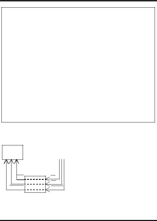
#9 |
STANDARD INTERRUPT ENABLE REGISTER |
|
|
|
|
|||
|
15 |
14 |
13 |
12 |
11 |
10 |
9 |
8 |
|
UNUSED |
UNUSED |
UNUSED |
UNUSED |
UNUSED |
UNUSED |
UNUSED |
UNUSED |
|
7 |
6 |
5 |
4 |
3 |
2 |
1 |
0 |
|
UNUSED |
UNUSED |
ILLBCMD |
ILLCMD |
POLFAIL |
RTYFAIL |
MSGERR |
CMDBLK |
#10 REMOTE TERMINAL ADDRESS REGISTER |
|
|
|
|
||||
|
15 |
14 |
13 |
12 |
11 |
10 |
9 |
8 |
|
INSTR |
BUSY2 |
SS FLAG |
DBC |
RT FLAG |
SRQ |
BUSY1 |
BC/RT |
|
7 |
6 |
5 |
4 |
3 |
2 |
1 |
0 |
|
LOCK |
PARERR |
RTAPAR |
RTA4 |
RTA3 |
RTA2 |
RTA1 |
RTA0 |
#11 BUILT-IN-TEST START REGISTER |
|
|
|
|
|
|||
|
15 |
14 |
13 |
12 |
11 |
10 |
9 |
8 |
|
X |
X |
X |
X |
X |
X |
X |
X |
|
7 |
6 |
5 |
4 |
3 |
2 |
1 |
0 |
|
X |
X |
X |
X |
X |
X |
X |
X |
#12 |
PROGRAMMED RESET REGISTER |
|
|
|
|
|
||
|
15 |
14 |
13 |
12 |
11 |
10 |
9 |
8 |
|
X |
X |
X |
X |
X |
X |
X |
X |
|
7 |
6 |
5 |
4 |
3 |
2 |
1 |
0 |
|
X |
X |
X |
X |
X |
X |
X |
X |
#13 REMOTE TERMINAL TIMER RESET REGISTER |
|
|
|
|
||||
|
15 |
14 |
13 |
12 |
11 |
10 |
9 |
8 |
|
X |
X |
X |
X |
X |
X |
X |
X |
|
7 |
6 |
5 |
4 |
3 |
2 |
1 |
0 |
|
X |
X |
X |
X |
X |
X |
X |
X |
X= DON’T CARE
Table 1. BCRT Registers (continued from page 16)
RAM |
CPU MEMORY |
|
CONTROL SIGNALS |
RRD |
BCRT |
RD |
|
RWR |
WR |
MEMCSO |
MEMCSI |
4.0 SYSTEM OVERVIEW
The BCRT can be configured for a variety of processor and memory environments. The host processor and the BCRT communicate via a flexible, programmable interrupt structure, internal registers, and a user-definable shared memory area. The shared memory area (up to 64K) is completely user-programmable and communicates BCRT control information -- message data, and
status/error information.
Figure 3a. Pseudo DualX0106Port RAM
Control Signals
BCRT-18

Built-in memory management functions designed specifically for MIL-STD-1553B applications aid processor off-loading. The host needs only to establish the parameters within memory so the BCRT can access this information as required. For example, in the RT mode, the BCRT can store data associated with individual subaddresses anywhere within its 64K address space. The BCRT then can automatically buffer up to 128 incoming messages of the same subaddress, thus preventing the previous messages from being overwritten by subsequent messages. This buffering also extends the intervals required by the host processor to service the data. Selecting an appropriate MCLK frequency to meet system memory access time requirements controls the memory access rate. The completion of a user-defined task or the occurrence of a user-selected event is indicated by using the extensive set of interrupts provided.
In the BC mode, the BCRT can process multiple messages, assist in scheduling message lists, and provide hostprogrammable functions such as auto retry. The BCRT is incorporated in systems with a variety of interrupt latencies by using the Interrupt History List feature (see Exception Handling and Interrupt Logging, page 33). The Interrupt History List sequentially stores the events that caused the interrupt in memory without losing information if a host processor does not respond immediately to an interrupt.
5.0SYSTEM INTERFACE
5.1DMA Transfers
The BCRT initiates DMA transfers whenever it executes command blocks (BC mode) or services commands (RT mode). DMAR initiates the transfer and is terminated by the inactive edge of DMACK. The Address Enable (AEN) input enables the BCRT to output an address onto the Address bus.
The BCRT requests transfer cycles by asserting the DMAR output, and initiates them when a DMAG input is received. A DMACK output indicates
that the BCRT has control of the Data and Address buses. The TSCTL output is asserted when the BCRT is actually asserting the Address and Data buses.
To support using multiple bus masters in a system, the BCRT outputs the DMAGO signal that results from the
DMAG signal passing through the chip when a BCRT bus request was not generated (DMAR inactive). You can use DMAGO in daisy-chained multimaster systems.
5.2 Hardware Interface
The BCRT provides a simple subsystem interface and facilitates DMA arbitration. The user can configure the BCRT to operate in a variety of memory-processor environments including the pseudo-dual-port RAM and standard DMA configurations.
For complete circuit description, such as arbitration logic and I/O, please refer to the appropriate application note.
5.3 CPU Interconnection
Pseudo-Dual-Port RAM Configuration
The BCRT’s Address and Data buses connect directly to RAM, with buffers isolating the BCRT’s buses from those of the host CPU (figures 3a and 3b). The CPU’s memory control signals (RD, WR, and MEMCSI) pass through the BCRT and connect to memory as RRL, RWR,
and MEMCSO.
Standard DMA Configuration
The BCRT’s and CPU’s data, address, and control signals are connected to each other as shown in figures 3c and 3d. The RWR, RRL, and MEMCSO are activated after DMAG is asserted.
In either case, the BCRT’s Address and Data buses remain in a high-impedance state unless the CS and RD signals are
active, indicating a host register access; or TSCTL is asserted, indicating a memory access by the BCRT. CPU attempts to access BCRT registers are ignored during BCRT memory access. Inhibit DMA transfers by using the Busy function in the Remote Terminal Address Register while operating in the Remote Terminal mode.
The designer can use TSCTL to indicate when the BCRT is accessing memory. AEN is also available (use is optional), giving the CPU control over the BCRT’s Address bus. A DMA Burst (BURST) signal indicates multiple
DMA accesses.
Register Access
Registers 0 through 13 are accessed with the decode of the four LSBs of the Address bus (A0-A3) and asserting CS. Pulse either RD or WR for multiple register accesses
BCRT-19
 Loading...