


UTMC 5962R9563801VYX, 5962R9563801VYC, 5962R9563801VYA, 5962R9563801VQX, 5962R9563801VQA Datasheet
...
Standard Products
UT69RH051 Radiation-Hardened MicroController
Data Sheet
|
May 2003 |
|
FEATURES |
|
|
q Three 16-bit timer/counters |
q Flexible clock operation |
|
- High speed output |
||
- Compare/capture |
- 1Hz to 20MHz with external clock |
|
- Pulse width modulator |
- 2MHz to 20MHz using internal oscillator with external |
|
- Watchdog timer capabilities |
crystal |
|
q 256 bytes of on-chip data RAM |
q Radiation-hardened process and design; total dose irradia- |
|
q 32 programmable I/O lines |
tion testing MIL-STD-883 Method 1019 |
|
- Total dose: 1.0E6 rads(Si) |
||
q 7 interrupt sources |
||
- Latchup immune |
||
q Programmable serial channel with: |
q Packaging options: |
|
- Framing error detection |
- 40-pin 100-mil center DIP (0.600 x 2.00) |
|
- Automatic address recognition |
- 44-lead 25-mil center Flatpack (0.670 x 0.800) |
|
q TTL and CMOS compatible logic levels |
q Standard Microcircuit Drawing 5962-95638 available |
|
q 64K external data and program memory space |
||
- QML Q & V compliant |
||
q MCS-51 fully compatible instruction set |
|
|
|
|
RAMADDRESS |
REG ISTER |
|
PORT 0 |
PORT 2 |
|
|
|
|
|
|
DRIVERS |
DRIVERS |
|
|||
|
|
|
RAM |
PORT 0 |
PORT 2 |
|
|||
|
|
|
LATCH |
LATCH |
|
||||
|
|
|
|
PROGRAM |
|||||
|
|
|
|
|
|
|
|
|
|
|
|
|
|
|
|
|
|
|
ADDRESS |
|
|
|
|
|
|
|
|
|
REGISTER |
|
|
|
B |
ACC |
|
|
|
STACK |
BUFFER |
|
REGISTER |
|
|
|
|
POINTER |
|||
|
|
|
|
|
|
||||
|
|
|
|
TMP2 |
TMP1 |
SPECIAL FUNCTION |
PC |
||
|
|
|
|
|
|
|
|
REGISTERS, |
|
|
|
|
|
|
|
|
|
INCREMENTER |
|
|
|
|
|
|
ALU |
|
|
TIMERS, |
|
|
|
|
|
|
|
|
|
||
|
|
|
|
|
|
|
PCA, |
|
|
PSEN |
|
S EQUENCER |
INSTRUCTION REGISTER |
|
|
|
|
PROGRAM |
|
|
|
|
|
|
SERIAL PORT |
||||
|
PSW |
TMP3 |
|
|
COUNTER |
||||
|
MICRO- |
|
|
||||||
ALE |
|
|
|
||||||
|
|
|
|
|
|
||||
E A |
|
|
|
|
|
DPTR |
|||
RST |
|
PORT 1 |
|
|
|
PORT 3 |
|||
|
|
LATCH |
|
|
|
LATCH |
|||
|
|
|
|
|
|
|
|
||
|
OSC. |
|
|
PORT 1 |
|
|
|
PORT 3 |
|
|
|
|
|
|
DRIVERS |
|
|
|
DRIVERS |
|
XTAL1 |
|
XTAL2 |
|
|
|
|
|
|
|
|
|
|
|
P1.0 - P1.7 |
|
|
|
P3.0 - P3.7 |
Figure 1. UT69RH051 MicroController Block Diagram
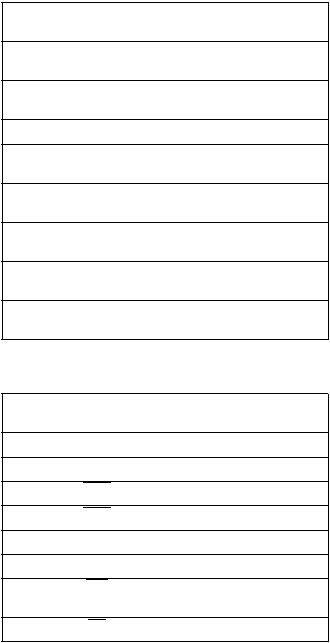
1.0 INTRODUCTION
The UT69RH051 is a radiation-tolerant 8-bit microcontroller that is pin equivalent to the MCS-51 industry standard microcontroller when in a 40-pin DIP. The UT69RH051’s static design allows operation from 1Hz to 20MHz. This data sheet describes hardware and software interfaces to the UT69RH051.
2.0 SIGNAL DESCRIPTION
VDD: +5V Supply voltage
VSS: Circuit Ground
Port 0 (P0.0 - P0.7): Port 0 is an 8-bit port. Port 0 pins are used as the low-order multiplexed address and data bus during accesses to external program and data memory. Port 0 pins use internal pullups when emitting 1’s and are TTL compatible.
Port 1 (P1.0 - P1.7):Port 1 is an 8-bit bidirectional I/O port with internal pullups. The output buffers can drive TTL loads. When the Port 1 pins have 1’s written to them, they are pulled high by the internal pullups and can be used as inputs in this state. As inputs, any pins that are externally pulled low sources current because of the pullups. In addition, Port 1 pins have the alternate uses shown in table 1.
Port 2 (P2.0 - P2.7): Port 2 is an 8-bit port. Port 2 pins are used as the high-order address bus during accesses to external Program Memory and during accesses to external Data Memory that uses 16-bit addresses (i.e., MOVX@DPTR). Port 2 uses internal pullups when emitting 1’s in this mode. During operations that do not require a 16-bit address, Port 2 emits the contents of the P2 Special Function Registers (SFR). The pins have internal pullups and drives TTL loads.
Port 3 (P3.0 - P3.7):Port 3 is an 8-bit bidirectional I/O port with internal pullups. The output buffers can drive TTL loads. When the Port 3 pins have 1’s written to them, they are pulled high by the internal pullups and can be used as inputs in this state. As inputs, any pins that are externally pulled low sources current because of the pullups. In addition, Port 3 pins have the alternate uses shown in table 2.
|
|
Table 1. Port 1 Alternate Functions |
||
Port |
|
Alternate |
|
Alternate Function |
|
|
|||
Pin |
|
Name |
|
|
P1.0 |
|
T2 |
|
External clock input to Timer/ |
|
|
|
|
Counter 2 |
P1.1 |
|
T2EX |
|
Timer/Counter 2 Capture/Reload |
|
|
|
|
trigger and direction control |
P1.2 |
|
ECI |
|
External count input to PCA |
P1.3 |
|
CEX0 |
|
External I/O for PCA capture/ |
|
|
|
|
compare Module 0 |
P1.4 |
|
CEX1 |
|
External I/O for PCA capture/ |
|
|
|
|
compare Module 1 |
P1.5 |
|
CEX2 |
|
External I/O for PCA capture/ |
|
|
|
|
compare Module 2 |
P1.6 |
|
CEX3 |
|
External I/O for PCA capture/ |
|
|
|
|
compare Module 3 |
P1.7 |
|
CEX4 |
|
External I/O for PCA capture/ |
|
|
|
|
compare Module 4 |
|
|
|
|
|
|
|
Table 2. Port 3 Alternate Functions |
||
Port |
|
Alternate |
|
Alternate Function |
|
|
|||
Pin |
|
Name |
|
|
P3.0 |
|
RXD |
|
Serial port input |
P3.1 |
|
TXD |
|
Serial port output |
P3.2 |
|
INT0 |
|
External interrupt 0 |
P3.3 |
|
INT1 |
|
External interrupt 1 |
P3.4 |
|
T0 |
|
External clock input for Timer 0 |
P3.5 |
|
T1 |
|
External clock input for Timer 1 |
P3.6 |
|
WR |
|
External Data Memory write |
|
|
|
|
strobe |
P3.7 |
|
RD |
|
External Data Memory read strobe |
|
|
|
|
|
2

RST: Reset Input. A high on this input for 24 oscillator periods while the oscillator is running resets the device. All ports and SFRs reset to their default conditions. Internal data memory is undefined after reset. Program execution begins within 12 oscillator periods (one machine cycle) after the RST signal is brought low. RST contains an internal pulldown resistor to allow implementing power-up reset with only an external capacitor.
ALE: Address Latch Enable. The ALE output is a pulse for latching the low byte of the address during accesses to external memory. In normal operation, the ALE pulse is output every sixth oscillator cycle and may be used for external timing or clocking. However, during each access to external Data Memory (MOVX instruction), one ALE pulse is skipped.
PSEN: Program Store Enable. This active low signal is the read strobe to the external program memory. PSEN activates every sixth oscillator cycle except that two PSEN activations are skipped during external data memory accesses.
EA: External Access Enable. This pin should be strapped to VSS (Ground) for the UT69RH051.
XTAL1: Input to the inverting oscillator amplifier.
XTAL2: Output from the inverting oscillator amplifier.
2.1 Hardware/Software Interface
2.1.1 Memory
The UT69RH051 has a separate address space for Program and Data Memory. Internally, the UT69RH051 contains 256 bytes of Data Memory. It addresses up to 64Kbytes of external Data Memory and 64Kbytes of external Program Memory.
2.1.1.1 Program Memory
There is no internal program memory in the UT69RH051. All program memory is accessed as external through ports P0 and P2. The EA pin must be tied to VSS (ground) to enable access to external locations 0000H through 7FFFH. Following reset, the UT69RH051 fetches the first instruction at address 0000h.
2.1.1.2 Data Memory
The UT69RH051 implements 256 bytes of internal data RAM. The upper 128 bytes of this RAM occupy a parallel address space to the SFRs. The CPU determines if the internal access to an address above 7FH is to the upper 128 bytes of RAM or to the SFR space by the addressing mode of the instruction. If direct addressing is used, the access is to the SFR space. If indirect addressing is used, the access is to the internal RAM. Stack operations are indirectly addressed so the upper portion of RAM can be used as stack space. Figure 3 shows the organization of the internal Data Memory.
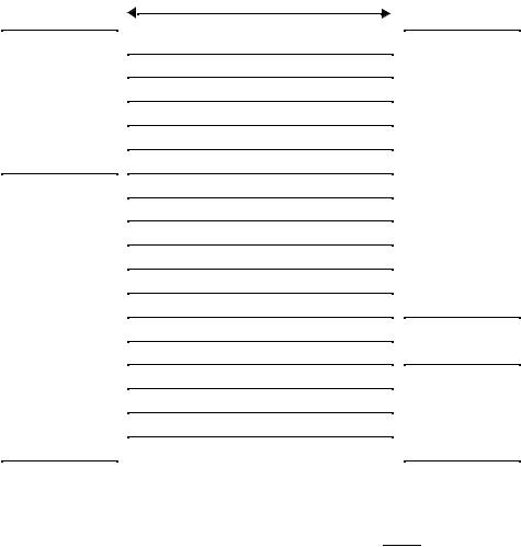
The first 32 bytes are reserved for four register banks of eight bytes each. The processor uses one of the four banks as its working registers depending on the RS1 and RS0 bits in the PSW SFR. At reset, bank 0 is selected. If four register banks are not required, use the unused banks as general purpose scratch pad memory. The next 16 bytes (128 bits) are individually bit addressable. The remaining bytes are byte addressable and can be used as general purpose scratch pad memory. For addresses 0 - 7FH, use either direct or indirect addressing. For addresses larger than 7FH, use only indirect addressing.
In addition to the internal Data Memory, the processor can access 64Kbytes of external Data Memory. The MOVX instruction accesses external Data Memory.
2.1.2 Special Function Registers
Table 3 contains the SFR memory map. Unoccupied addresses are not implemented on the device. Read accesses to these addresses will return unknown values and write accesses will have no effect.
3
(T2) |
P1.0 |
|
1 |
40 |
|
VDD |
|
|
|
|
|||||
|
|
|
|||||
(T2EX) |
P1.1 |
|
2 |
39 |
|
P0.0 |
(AD0) |
|
|
||||||
(ECI) |
P1.2 |
|
3 |
38 |
|
P0.1 |
(AD1) |
|
|
||||||
(CEX0) |
P1.3 |
|
4 |
37 |
|
P0.2 |
(AD2) |
|
|
||||||
(CEX1) |
P1.4 |
|
5 |
36 |
|
P0.3 |
(AD3) |
|
|
||||||
(CEX2) |
P1.5 |
|
6 |
35 |
|
P0.4 |
(AD4) |
|
|
||||||
(CEX3) |
P1.6 |
|
7 |
34 |
|
P0.5 |
(AD5) |
|
|
||||||
(CEX4) |
P1.7 |
|
8 |
33 |
|
P0.6 |
(AD6) |
|
|
||||||
|
RST |
|
9 |
32 |
|
P0.7 |
(AD7) |
|
|
|
|||||
(RXD) |
P3.0 |
|
10 |
31 |
|
EA |
|
|
|
|
|||||
(TXD) |
P3.1 |
|
11 |
30 |
|
ALE |
|
|
|
|
|||||
(INT0) |
P3.2 |
|
12 |
29 |
|
PSEN |
|
|
|
|
|||||
(INT1) |
P3.3 |
|
13 |
28 |
|
P2.7 |
(A15) |
|
|
||||||
(T0) |
P3.4 |
|
14 |
27 |
|
P2.6 |
(A14) |
|
|
||||||
(T1) |
P3.5 |
|
15 |
26 |
|
P2.5 |
(A13) |
|
|
||||||
(WR) |
P3.6 |
|
16 |
25 |
|
P2.4 |
(A12) |
|
|
||||||
(RD) |
P3.7 |
|
17 |
24 |
|
P2.3 |
(A11) |
|
|
||||||
|
XTAL2 |
|
18 |
23 |
|
P2.2 |
(A10) |
|
|
|
|||||
|
XTAL1 |
|
19 |
22 |
|
P2.1 |
(A9) |
|
|
|
|||||
|
V SS |
|
20 |
21 |
|
P2.0 |
(A8) |
|
|
|
Figure 2a. UT69RH051 40-Pin DIP Connections
|
VSS |
|
1 |
44 |
|
VDD |
|
|
|
|
|
||||
|
|
|
|
||||
(T2) |
P1.0 |
|
2 |
43 |
|
P0.0 |
(AD0) |
|
|
||||||
(T2EX) |
P1.1 |
|
3 |
42 |
|
P0.1 |
(AD1) |
|
|
||||||
|
NC |
|
4 |
41 |
|
P0.2 |
(AD2) |
|
|
|
|||||
(ECI) |
P1.2 |
|
5 |
40 |
|
P0.3 |
(AD3) |
|
|
||||||
(CEX0) |
P1.3 |
|
6 |
39 |
|
P0.4 |
(AD4) |
|
|
||||||
(CEX1) |
P1.4 |
|
7 |
38 |
|
P0.5 |
(AD5) |
|
|
||||||
(CEX2) |
P1.5 |
|
8 |
37 |
|
P0.6 |
(AD6) |
|
|
||||||
(CEX3) |
P1.6 |
|
9 |
36 |
|
P0.7 |
(AD7) |
|
|
||||||
(CEX4) |
P1.7 |
|
10 |
35 |
|
EA |
|
|
|
|
|||||
|
RST |
|
11 |
34 |
|
ALE |
|
|
|
|
|
||||
(RXD) |
P3.0 |
|
12 |
33 |
|
PSEN |
|
|
|
|
|||||
(TXD) |
P3.1 |
|
13 |
32 |
|
P2.7 |
(A15) |
|
|
||||||
(INTO ) |
P3.2 |
|
14 |
31 |
|
P2.6 |
(A14) |
|
|
||||||
(INT1) |
P3.3 |
|
15 |
30 |
|
P2.5 |
(A13) |
|
|
||||||
(TO) |
P3.4 |
|
16 |
29 |
|
P2.4 |
(A12) |
|
|
||||||
(T1) |
P3.5 |
|
17 |
28 |
|
P2.3 |
(A11) |
|
|
||||||
(WR) |
P3.6 |
|
18 |
27 |
|
P2.2 |
(A10) |
|
|
||||||
(RD) |
P3.7 |
|
19 |
26 |
|
P2.1 |
(A9) |
|
|
||||||
|
XTAL2 |
|
20 |
25 |
|
P2.0 |
(A8) |
|
|
|
|||||
|
XTAL1 |
21 |
24 |
|
NC |
|
|
|
|
|
|||||
|
VSS |
22 |
23 |
|
VDD |
|
|
|
|
|
|||||
Figure 2b. UT69RH051 44-Pin Flatpack Connections
4
|
F8 |
|
8 BYTES |
|
FF |
|
|
|
|
|
|||
|
|
|
|
|
||
|
|
|
|
|
||
|
|
|
|
|
||
|
F0 |
|
|
|
F7 |
|
INDIRECT |
∙ |
|
|
|
∙ |
|
ACCESS |
∙ |
|
|
|
∙ |
|
ONLY |
|
|
|
|
||
∙ |
|
|
|
∙ |
|
|
|
|
|
|
|
||
|
88 |
|
|
|
8F |
SCRATCH |
|
|
|
|
|
|
|
|
80 |
|
|
|
87 |
PAD AREA |
|
|
|
|
|
||
|
78 |
|
|
|
7F |
|
|
70 |
|
|
|
77 |
|
|
∙ |
|
|
|
∙ |
|
|
∙ |
|
|
|
∙ |
|
|
∙ |
|
|
|
∙ |
|
|
38 |
|
|
|
3F |
|
DIRECT OR |
30 |
|
|
|
37 |
|
INDIRECT |
28 |
|
|
|
2F |
BIT |
ACCESS |
|
|
|
|||
|
|
|
ADDRESSABLE |
|||
|
20 |
|
|
|
27 |
|
|
|
|
|
SEGMENT |
||
|
|
|
|
|
|
|
|
18 |
|
|
|
1F |
|
|
10 |
|
|
|
17 |
REGISTER |
|
08 |
|
|
|
0F |
BANKS |
|
|
|
|
|
||
|
00 |
|
|
|
07 |
|
|
|
|
|
|
|
|
Figure 3. Internal Data Memory Organization
2.1.3 Reset
The reset input is the RST pin. To reset, hold the RST pin high for a minimum of 24 oscillator periods while the oscillator is running. The CPU generates an internal reset from the external signal. The port pins are driven to the reset state as soon as a valid high is detected on the RST pin.
While RST is high,PSEN and the port pins are pulled high; ALE is pulled low. All SFRs are reset to their reset values as shown in table 3. The internal Data Memory content is indeterminate.
The processor will begin operation one machine cycle after the RST line is brought low. A memory access occurs immediately after the RST line is brought low, but the data is not brought into the processor. The memory access repeats on the next machine cycle and actual processing begins at that time.
5

Table 3. SFR Memory Registers
F8 |
|
CH |
CCAP0H |
CCAP1H |
CCAP2H |
CCAP3H |
CCAP4H |
|
FF |
|
|
00000000 |
XXXXXXXX |
XXXXXXXX |
XXXXXXXX |
XXXXXXXX |
XXXXXXXX |
|
|
F0 |
B |
|
|
|
|
|
|
|
F7 |
|
00000000 |
|
|
|
|
|
|
|
|
E8 |
|
CL |
CCAP0L |
CCAP1L |
CCAP2L |
CCAP3L |
CCAP4L |
|
EF |
|
|
00000000 |
XXXXXXXX |
XXXXXXXX |
XXXXXXXX |
XXXXXXXX |
XXXXXXXX |
|
|
E0 |
ACC |
|
|
|
|
|
|
|
E7 |
|
00000000 |
|
|
|
|
|
|
|
|
D8 |
CCON |
CMOD |
CCAPM0 |
CCAPM1 |
CCAPM2 |
CCAPM3 |
CCAPM4 |
|
DF |
|
00X00000 |
OOXXX000 |
X00000000 |
X00000000 |
X00000000 |
X00000000 |
X00000000 |
|
|
D0 |
PSW |
|
|
|
|
|
|
|
D7 |
|
00000000 |
|
|
|
|
|
|
|
|
C8 |
T2CON |
T2MOD |
RCAP2L |
RCAP2H |
TL2 |
TH2 |
|
|
CF |
|
00000000 |
XXXXXX00 |
00000000 |
00000000 |
00000000 |
00000000 |
|
|
|
C0 |
|
|
|
|
|
|
|
|
C7 |
B8 |
IP |
SADEN |
|
|
|
|
|
|
BF |
|
X0000000 |
00000000 |
|
|
|
|
|
|
|
B0 |
P3 |
|
|
|
|
|
|
IPH |
B7 |
|
11111111 |
|
|
|
|
|
|
X00000000 |
|
A8 |
IE |
SADDR |
|
|
|
|
|
|
AF |
|
00000000 |
00000000 |
|
|
|
|
|
|
|
A0 |
P2 |
|
|
|
|
|
|
|
A7 |
|
11111111 |
|
|
|
|
|
|
|
|
98 |
SCON |
SBUF |
|
|
|
|
|
|
9F |
|
00000000 |
XXXXXXXX |
|
|
|
|
|
|
|
90 |
P1 |
|
|
|
|
|
|
|
97 |
|
11111111 |
|
|
|
|
|
|
|
|
88 |
TCON |
TMOD |
TL0 |
TL1 |
TH0 |
TH1 |
|
|
8F |
|
00000000 |
00000000 |
00000000 |
00000000 |
00000000 |
00000000 |
|
|
|
80 |
P0 |
SP |
DPL |
DPH |
|
|
|
PCON |
87 |
|
11111111 |
00000111 |
00000000 |
00000000 |
|
|
|
00XX00XX |
|
|
|
|
|
|
|
|
|
|
|
Notes:
1.Values shown are the reset values of the registers.
2.X = undefined.
6
 Loading...