


UNITRODE UC1714, UC1715, UC2714, UC2715, UC3714 Technical data
...
UC3714DP
application
INFO
available
UC1714/5
UC2714/5
UC3714/5
Complementary Switch FET Drivers
FEATURES
•Single Input (PWM and TTL Compatible)
•High Current Power FET Driver, 1.0A Source/2A Sink
•Auxiliary Output FET Driver, 0.5A Source/1A Sink
•Time Delays Between Power and Auxiliary Outputs Independently Programmable from 50ns to 500ns
•Time Delay or True Zero-Voltage Operation Independently Configurable for Each Output
•Switching Frequency to 1MHz
•Typical 50ns Propagation Delays
•ENBL Pin Activates 220 A Sleep Mode
•Power Output is Active Low in Sleep Mode
DESCRIPTION
These two families of high speed drivers are designed to provide drive waveforms for complementary switches. Complementary switch configurations are commonly used in synchronous rectification circuits and active clamp/reset circuits, which can provide zero voltage switching. In order to facilitate the soft switching transitions, independently programmable delays between the two output waveforms are provided on these drivers. The delay pins also have true zero voltage sensing capability which allows immediate activation of the corresponding switch when zero voltage is applied. These devices require a PWM-type input to operate and can be interfaced with commonly available PWM controllers.
In the UC1714 series, the AUX output is inverted to allow driving a p-channel MOSFET. In the UC1715 series, the two outputs are configured in a true complementary fashion.
• Synchronous Rectifier Driver
BLOCK DIAGRAM
|
|
50ns –500ns |
|
|
2 |
PWR |
INPUT |
6 |
TIMER |
|
|
|
|
S |
|
|
|
|
||
|
|
|
|
|
|
|
|
|
Q |
|
|
|
|
T1 |
7 |
R |
|
UC1714 |
|
|
|
|
VREF |
|
ONLY |
|
|
|
|
50ns –500ns |
|
|
4 |
AUX |
|
|
|
|
|
|
|
|
|
TIMER |
|
|
1 |
VCC |
|
|
S |
|
|
||
|
|
|
|
|
|
|
|
|
Q |
VCC |
5V |
LOGIC |
|
|
|
|
|
|||
T2 |
5 |
R |
BIAS |
GATES |
|
|
|
|
|||||
|
|
VREF |
|
|
||
|
|
ENBL |
3V |
TIMER |
|
|
|
|
|
GND |
REF |
|
|
|
|
|
|
|
||
|
|
|
|
|
3 |
GND |
|
|
1.4V |
|
|
|
|
ENBL |
8 |
|
|
|
|
|
|
|
ENABLE |
|
|
|
|
J, N and D packages.
UDG-99028
1999 - REVISED JANUARY 2002
UC1714/5
UC2714/5
UC3714/5
ABSOLUTE MAXIMUM RATINGS
Supply Voltage VCC . . . . . . . . . . . . . . . . . . . . . . . . . . . . . . . 20V Power Driver IOH
continuous . . . . . . . . . . . . . . . . . . . . . . . . . . . . . . . . −200mA peak. . . . . . . . . . . . . . . . . . . . . . . . . . . . . . . . . . . . . . . . . −1A
Power Driver IOL
continuous . . . . . . . . . . . . . . . . . . . . . . . . . . . . . . . . . 400mA peak. . . . . . . . . . . . . . . . . . . . . . . . . . . . . . . . . . . . . . . . . . 2A
Auxiliary Driver IOH
continuous . . . . . . . . . . . . . . . . . . . . . . . . . . . . . . . . −100mA peak . . . . . . . . . . . . . . . . . . . . . . . . . . . . . . . . . . . . . −500mA
Auxiliary Driver IOL
continuous . . . . . . . . . . . . . . . . . . . . . . . . . . . . . . . . . 200mA peak. . . . . . . . . . . . . . . . . . . . . . . . . . . . . . . . . . . . . . . . . . 1A
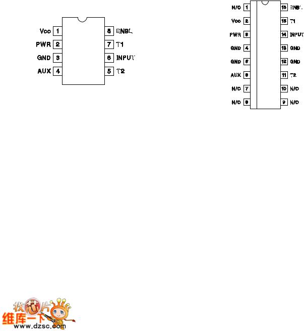
CONNECTION DIAGRAMS
Input Voltage Range (INPUT, ENBL) . . . . . . . . . . −0.3V to 20V Storage Temperature Range . . . . . . . . . . . . . . −65°C to 150°C Operating Junction Temperature (Note 1) . . . . . . . . . . . . 150°C Lead Temperature (Soldering 10 seconds) . . . . . . . . . . . 300°C
Note 1: Unless otherwise indicated, voltages are referenced to ground and currents are positive into, negative out of, the specified terminals.
Note 2: Consult Packaging Section of databook for thermal limitations and specifications of packages.
DIL-8, SOIC-8 (Top View) |
|
|
|
|
|
|
|
|
|
SOIC-16 (Top View) |
|||||||
J or N, D Packages |
|
|
|
|
|
|
|
|
|
DP Package |
|||||||
|
|
|
|
|
|
|
|
|
|
|
|
|
|
|
|
|
|
|
|
|
|
|
|
|
|
|
|
|
|
|
|
|
|
|
|
|
|
|
|
|
|
|
|
|
|
|
|
|
|
|
|
|
|
|
|
|
|
|
|
|
|
|
|
|
|
|
|
|
|
|
|
|
|
|
|
|
|
|
|
|
|
|
|
|
|
|
|
|
|
|
|
|
|
|
|
|
|
|
|
|
|
|
|
|
|
|
|
|
|
|
|
|
|
|
|
|
|
|
|
|
|
|
|
|
|
|
|
|
|
|
|
|
|
|
|
|
|
|
|
|
|
|
|
|
|
|
|
|
|
|
|
|
|
|
|
|
|
|
|
|
|
|
|
|
|
|
|
|
|
|
|
|
|
|
|
|
|
|
|
|
|
|
|
|
|
|
|
|
|
|
|
|
|
|
|
|
|
|
|
|
|
|
|
|
|
|
|
|
|
|
|
|
|
|
|
|
|
|
|
|
|
|
|
|
|
|
|
|
|
|
|
|
|
ELECTRICAL CHARACTERISTICS: Unless otherwise stated, VCC = 15V, ENBL ≥ 2V, RT1 = 100kΩ from T1 to GND, RT2 = 100kΩ from T2 to GND, and −55°C < TA < 125°C for the UC1714/5, −40°C < TA < 85°C for the UC2714/5, and 0°C < TA < 70°C for the UC3714/5, TA = TJ.
PARAMETER |
TEST CONDITIONS |
MIN |
TYP |
MAX |
UNITS |
Overall |
|
|
|
|
|
VCC |
|
7 |
|
20 |
V |
ICC, nominal |
ENBL = 2.0V |
|
18 |
24 |
mA |
ICC, sleep mode |
ENBL = 0.8V |
|
200 |
300 |
µA |
Power Driver (PWR) |
|
|
|
|
|
Pre Turn-on PWR Output, Low |
VCC = 0V, IOUT = 10mA, ENBL 0.8V |
|
0.3 |
1.6 |
V |
PWR Output Low, Sat. (VPWR) |
INPUT = 0.8V, IOUT = 40mA |
|
0.3 |
0.8 |
V |
|
INPUT = 0.8V, IOUT = 400mA |
|
2.1 |
2.8 |
V |
PWR Output High, Sat. (VCC − VPWR) |
INPUT = 2.0V, IOUT = −20mA |
|
2.1 |
3 |
V |
|
INPUT = 2.0V, IOUT = −200mA |
|
2.3 |
3 |
V |
Rise Time |
CL = 2200pF |
|
30 |
60 |
ns |
Fall Time |
CL = 2200pF |
|
25 |
60 |
ns |
T1 Delay, AUX to PWR |
INPUT rising edge, RT1 = 10kΩ (Note 4) |
20 |
35 |
80 |
ns |
T1 Delay, AUX to PWR |
INPUT rising edge, RT1 = 100kΩ (Note 4) |
350 |
500 |
700 |
ns |
|
INPUT falling edge, 50% (Note 3) |
|
35 |
100 |
ns |
2

UC1714/5
UC2714/5
UC3714/5
ELECTRICAL CHARACTERISTICS: Unless otherwise stated, VCC = 15V, ENBL ≥ 2V, RT1 = 100kΩ from T1 to GND, RT2 = 100kΩ from T2 to GND, and −55°C < TA < 125°C for the UC1714/5, −40°C < TA < 85°C for the UC2714/5, and 0°C < TA < 70°C for the UC3714/5, TA = TJ.
PARAMETER |
TEST CONDITIONS |
MIN |
TYP |
MAX |
UNITS |
|
Auxiliary Driver (AUX) |
|
|
|
|
|
|
AUX Output Low, Sat |
(VAUX) |
VIN = 2.0V, IOUT = 20mA |
|
0.3 |
0.8 |
V |
|
|
VIN = 2.0V, IOUT = 200mA |
|
1.8 |
2.6 |
V |
AUX Output High, Sat |
(VCC – VAUX) |
VIN = 0.8V, IOUT = -10mA |
|
2.1 |
3.0 |
V |
|
|
VIN = 0.8V, IOUT = -100mA |
|
2.3 |
3.0 |
V |
Rise Time |
|
CL = 1000pF |
|
45 |
60 |
ns |
Fall Time |
|
CL = 1000pF |
|
30 |
60 |
ns |
T2 Delay, PWR to AUX |
|
INPUT falling edge, RT2 = 10kΩ (Note 4) |
20 |
50 |
80 |
ns |
T2 Delay, PWR to AUX |
|
INPUT falling edge, RT2 = 100kΩ (Note 4) |
250 |
350 |
550 |
ns |
AUX Prop Delay |
|
INPUT rising edge, 50% (Note 3) |
|
35 |
80 |
ns |
Enable (ENBL) |
|
|
|
|
|
|
Input Threshold |
|
|
0.8 |
1.2 |
2.0 |
V |
Input Current, IIH |
|
ENBL = 15V |
|
1 |
10 |
µA |
Input Current, IIL |
|
ENBL = 0V |
|
−1 |
−10 |
µA |
T1 |
|
|
|
|
|
|
Current Limit |
|
T1 = 0V |
|
−1.6 |
−2 |
mA |
Nominal Voltage at T1 |
|
|
2.7 |
3 |
3.3 |
V |
Minimum T1 Delay |
|
T1 = 2.5V, (Note 4) |
|
40 |
70 |
ns |
T2 |
|
|
|
|
|
|
Current Limit |
|
T2 = 0V |
|
−1.2 |
−2 |
mA |
Nominal Voltage at T2 |
|
|
2.7 |
3 |
3.3 |
V |
Minumum T2 Delay |
|
T2 = 2.5V, (Note 4) |
|
50 |
100 |
ns |
Input (INPUT) |
|
|
|
|
|
|
Input Threshold |
|
|
0.8 |
1.4 |
2.0 |
V |
Input Current, IIH |
|
INPUT = 15V |
|
1 |
10 |
µA |
Input Current, IIL |
|
INPUT = 0V |
|
−5 |
−20 |
µA |
Note 3: Propagation delay times are measured from the 50% point of the input signal to the 10% point of the output signal’s transition with no load on outputs.
Note 4: T1 delay is defined from the 50% point of the transition edge of AUX to the 10% of the rising edge of PWR. T2 delay is defined from the 90% of the falling edge of PWR to the 50% point of the transition edge of AUX.
PIN DESCRIPTIONS
AUX: The AUX switches immediately at INPUT’s rising edge but waits through the T2 delay after INPUT’s falling edge before switching. AUX is capable of sourcing 0.5A and sinking 1.0A of drive current. See the Time Relationships diagram below for the difference between the UC1714 and UC1715 for INPUT, MAIN, and AUX. During sleep mode, AUX is inactive with a high impedance.
switches at TTL logic levels (apinput range is from 0V to 20V.
The ENBL input will place the device into sleep mode when it is a logical low. The current into VCC during the sleep mode is typically 220 A.
GND: This is the reference pin for all input voltages and the return point for all device currents. It carries the full peak sinking current from the outputs. Any tendency for the outputs to ring below GND voltage must be damped or clamped such that GND remains the most negative potential.
3
 Loading...