


XTR116 XTR115
XTR115
XTR116
SBOS124A – JANUARY 2000 – REVISED NOVEMBER 2003
4-20mA CURRENT LOOP TRANSMITTERS
FEATURES |
APPLICATIONS |
●LOW QUIESCENT CURRENT: 200 A
●5V REGULATOR FOR EXTERNAL CIRCUITS
●VREF FOR SENSOR EXCITATION:
XTR115: 2.5V
XTR116: 4.096V
●LOW SPAN ERROR: 0.05%
●LOW NONLINEARITY ERROR: 0.003%
●WIDE LOOP SUPPLY RANGE: 7.5V to 36V
●SO-8 PACKAGE
DESCRIPTION
The XTR115 and XTR116 are precision current output converters designed to transmit analog 4-to-20mA signals over an industry standard current loop. They provide accurate current scaling and output current limit functions.
The on-chip voltage regulator (5V) can be used to power external circuitry. A precision on-chip VREF (2.5V for XTR115 and 4.096V for XTR116) can be
●2-WIRE, 4-20mA CURRENT LOOP TRANSMITTER
●SMART TRANSMITTER
●INDUSTRIAL PROCESS CONTROL
●TEST SYSTEMS
●COMPATIBLE WITH HART MODEM
●CURRENT AMPLIFIER
●VOLTAGE-TO-CURRENT AMPLIFIER
used for offsetting or to excite transducers. A current return pin (IRET) senses any current used in external circuitry to assure an accurate control of the output current.
The XTR115 is a fundamental building block of smart sensors using 4-to-20mA current transmission.
The XTR115 and XTR116 are specified for operation over the extended industrial temperature range, –40° C to +85° C.
|
|
|
XTR115 |
|
|
|
|
|
|
|
|
XTR116 |
|
|
|
|
|
+5V |
|
VREG |
|
|
+5V |
V+ |
|
|
|
8 |
|
|
Regulator |
7 |
|
|
|
|
|
|
|
|
|
|||
XTR115: 2.5V |
|
VREF |
|
Voltage |
|
|
|
|
XTR116: 4.096V |
|
1 |
|
Reference |
|
|
|
|
|
|
|
|
|
|
|
|
VLOOP |
|
RIN |
|
|
|
|
B |
|
|
|
IIN |
|
|
|
6 |
|
|
|
|
|
|
|
|
|
|
||
+ |
|
2 |
|
A1 |
|
|
|
RL |
|
|
|
|
|
|
|||
|
|
|
|
|
|
|
||
VIN |
|
|
|
|
|
E |
|
|
– |
|
|
|
|
|
5 |
|
|
|
|
3 |
|
|
|
RLIM |
|
|
|
|
IRET |
R1 |
|
R2 |
I |
|
100 VIN |
|
|
|
|
O |
= |
|||
|
|
|
2.475kΩ |
25Ω |
|
RIN |
||
|
|
|
|
|
||||
|
|
|
|
|
|
4 |
|
|
|
|
|
|
|
|
|
|
I = 100 • IIN |
Please be aware that an important notice concerning availability, standard warranty, and use in critical applications of Texas Instruments semiconductor products and disclaimers thereto appears at the end of this data sheet.
All trademarks are the property of their respective owners.
PRODUCTION DATA information is current as of publication date. |
Copyright © 2000-2003, Texas Instruments Incorporated |
Products conform to specifications per the terms of Texas Instruments |
|
standard warranty. Production processing does not necessarily include |
|
testing of all parameters. |
|
www.ti.com

SPECIFICATIONS
At TA = +25° C, V+ = 24V, RIN = 20kΩ , and TIP29C external transistor, unless otherwise noted.
|
|
|
|
|
|
XTR115U |
|
|
|
|
XTR115UA |
|
|
|
|
|
|
|
|
|
XTR116U |
|
|
|
|
XTR116UA |
|
|
|
|
|
|
|
|
|
|
|
|
|
|
|
|
|
|
PARAMETER |
|
CONDITIONS |
MIN |
|
TYP |
|
MAX |
MIN |
TYP |
MAX |
UNITS |
|||
|
|
|
|
|
|
|
|
|
|
|
|
|
|
|
OUTPUT |
|
|
|
|
|
|
|
|
|
|
|
|
|
|
Output Current Equation |
IO |
|
|
|
IO = IIN • 100 |
|
|
|
|
|
|
|
||
Output Current, Linear Range |
|
|
0.25 |
|
|
|
|
25 |
|
|
|
mA |
||
Over-Scale Limit |
ILIM |
|
|
|
|
32 |
|
|
|
|
|
|
|
mA |
Under-Scale Limit |
IMIN |
IREG = 0, IREF = 0 |
|
|
|
0.2 |
|
0.25 |
|
|
|
mA |
||
SPAN |
|
|
|
|
|
|
|
|
|
|
|
|
|
|
Span (Current Gain) |
S |
|
|
|
|
100 |
|
|
|
|
|
|
|
A/A |
Error (1) |
|
IIN = 250µ A to 25mA |
|
|
|
± 0.05 |
|
± |
0.2 |
|
|
± 0.4 |
% |
|
vs Temperature |
|
TA = –40° C to +85° C |
|
|
|
± 3 |
|
± 20 |
|
|
|
ppm/° C |
||
Nonlinearity |
|
IIN = 250µ A to 25mA |
|
|
|
± 0.003 |
|
± |
0.01 |
|
|
± 0.02 |
% |
|
INPUT |
|
|
|
|
|
|
|
|
|
|
|
|
|
|
Offset Voltage (Op Amp) |
VOS |
IIN = 40µ A |
|
|
|
± 100 |
|
± |
250 |
|
|
± 500 |
µ V |
|
vs Temperature |
|
TA = –40° C to +85° C |
|
|
|
± 0.7 |
|
|
± 3 |
|
|
± 6 |
µ V/° C |
|
vs Supply Voltage, V+ |
|
V+ = 7.5V to 36V |
|
|
|
± 0.1 |
|
|
± 2 |
|
|
|
µ V/V |
|
Bias Current |
IB |
|
|
|
|
–35 |
|
|
|
|
|
|
|
nA |
vs Temperature |
|
|
|
|
|
150 |
|
|
|
|
|
|
|
pA/° C |
Noise: 0.1Hz to 10Hz |
en |
|
|
|
|
0.6 |
|
|
|
|
|
|
|
µ Vp-p |
DYNAMIC RESPONSE |
|
|
|
|
|
|
|
|
|
|
|
|
|
|
Small Signal Bandwidth |
|
CLOOP = 0, RL = 0 |
|
|
|
380 |
|
|
|
|
|
|
|
kHz |
Slew Rate |
|
|
|
|
|
3.2 |
|
|
|
|
|
|
|
mA/µ s |
(2) |
|
|
|
|
|
|
|
|
|
|
|
|
|
|
VREF |
|
|
|
|
|
|
|
|
|
|
|
|
|
|
XTR115 |
|
|
|
|
|
2.5 |
|
|
|
|
|
|
|
V |
XTR116 |
|
|
|
|
|
4.096 |
|
|
|
|
|
|
|
V |
Voltage Accuracy |
|
IREF = 0 |
|
|
|
± 0.05 |
|
± |
0.25 |
|
|
± 0.5 |
% |
|
vs Temperature |
|
TA = –40° C to +85° C |
|
|
|
± 20 |
|
± 35 |
|
|
± 75 |
ppm/° C |
||
vs Supply Voltage, V+ |
|
V+ = 7.5V to 36V |
|
|
|
± 1 |
|
± 10 |
|
|
|
ppm/V |
||
vs Load |
|
IREF = 0mA to 2.5mA |
|
|
|
± 100 |
|
|
|
|
|
|
|
ppm/mA |
Noise: 0.1Hz to 10Hz |
|
|
|
|
|
10 |
|
|
|
|
|
|
|
µ Vp-p |
Short-Circuit Current |
|
|
|
|
|
16 |
|
|
|
|
|
|
|
mA |
|
|
|
|
|
|
|
|
|
|
|
|
|
|
|
(2) |
|
|
|
|
|
|
|
|
|
|
|
|
|
|
VREG |
|
|
|
|
|
|
|
|
|
|
|
|
|
|
Voltage |
|
|
|
|
|
5 |
|
|
|
|
|
|
|
V |
Voltage Accuracy |
|
IREG = 0 |
|
|
|
± 0.05 |
|
± |
0.1 |
|
|
|
V |
|
vs Temperature |
|
TA = –40° C to +85° C |
|
|
|
± 0.1 |
|
|
|
|
|
|
|
mV/° C |
vs Supply Voltage, V+ |
|
V+ = 7.5V to 36V |
|
|
|
1 |
|
|
|
|
|
|
|
mV/V |
vs Output Current |
|
|
|
See |
|
Typical Curves |
|
|
|
|
|
|
||
Short-Circuit Current |
|
|
|
|
|
12 |
|
|
|
|
|
|
|
mA |
|
|
|
|
|
|
|
|
|
|
|
|
|
|
|
POWER SUPPLY |
V+ |
|
|
|
|
|
|
|
|
|
|
|
|
|
Specified |
|
|
|
|
|
+24 |
|
|
|
|
|
|
|
V |
Voltage Range |
|
|
+7.5 |
|
|
|
+36 |
|
|
|
V |
|||
Quiescent Current |
|
|
|
|
|
200 |
|
250 |
|
|
|
µ A |
||
Over Temperature, –40° C to +85° C |
|
|
|
|
|
240 |
|
300 |
|
|
|
µ A |
||
|
|
|
|
|
|
|
|
|
|
|
|
|
|
|
TEMPERATURE RANGE |
|
|
|
|
|
|
|
|
|
|
|
|
|
|
Specification |
|
|
–40 |
|
|
|
+85 |
|
|
|
° C |
|||
Operating |
|
|
–55 |
|
|
|
+125 |
|
|
|
° C |
|||
Storage |
|
|
–55 |
|
|
|
+125 |
|
|
|
° C |
|||
Thermal Resistance |
θ JA |
|
|
|
|
150 |
|
|
|
|
|
|
|
° C/W |
Specifications the same as XTR115U and XTR116U.
NOTES: (1) Does not include initial error or TCR of RIN. (2) Voltage measured with respect to IRET pin.
2 |
XTR115, XTR116 |
www.ti.com |
SBOS124A |
PIN CONFIGURATION
Top View |
|
|
|
SO-8 |
|
|
|
|
|
VREF |
1 |
|
8 |
VREG |
|
|
|
|
|
IIN |
2 |
|
7 |
V+ |
|
|
|
|
|
IRET |
3 |
|
6 |
B (Base) |
|
|
|
|
|
IO |
4 |
|
5 |
E (Emitter) |
PACKAGE/ORDERING INFORMATION
For the most current package and ordering information, see the Package Option Addendum located at the end of this data sheet.
XTR115, XTR116
ABSOLUTE MAXIMUM RATINGS(1)
Power Supply, V+ (referenced to IO pin) |
.......................................... 40V |
Input Voltage (referenced to IRET pin) ........................................ |
0V to V+ |
Output Current Limit ............................................................... |
Continuous |
VREG, Short-Circuit .................................................................. |
Continuous |
VREF, Short-Circuit .................................................................. |
Continuous |
Operating Temperature ................................................ |
–55 ° C to +125° C |
Storage Temperature Range ....................................... |
–55 ° C to +125° C |
Lead Temperature (soldering, 10s) .............................................. |
+300° C |
Junction Temperature ................................................................... |
+165° C |
|
|
NOTE: (1) Stresses above these ratings may cause permanent damage. Exposure to absolute maximum conditions for extended periods may degrade device reliability.
ELECTROSTATIC DISCHARGE SENSITIVITY
This integrated circuit can be damaged by ESD. Texas Instruments recommends that all integrated circuits be handled with appropriate precautions. Failure to observe proper handling and installation procedures can cause damage.
ESD damage can range from subtle performance degradation to complete device failure. Precision integrated circuits may be more susceptible to damage because very small parametric changes could cause the device not to meet its published specifications.
3
SBOS124A |
www.ti.com |

TYPICAL PERFORMANCE CURVES
At TA = +25° C, V+ = 24V, RIN = 20kΩ , and TIP29C external transistor, unless otherwise noted.
CURRENT GAIN vs FREQUENCY
|
40 |
|
|
(dB) |
30 |
|
COUT = 0 |
|
|
RL = 0Ω |
|
Gain |
|
|
|
|
|
|
|
|
20 |
COUT = 10nF |
|
|
RL |
= 250Ω |
|
|
|
||
10
10k |
100k |
1M |
|
Frequency (Hz) |
|
QUIESCENT CURRENT vs TEMPERATURE
|
260 |
|
|
|
|
|
|
|
|
( A) |
240 |
|
|
|
|
|
|
|
|
|
|
|
|
(V+) = 36V |
|
|
|
||
Current |
|
|
|
|
|
|
|
||
220 |
|
|
|
|
|
|
|
|
|
|
|
|
|
|
|
|
(V+) = 24V |
|
|
Quiescent |
200 |
|
|
|
|
|
|
|
|
|
|
|
|
|
|
|
|
||
180 |
|
|
|
|
(V+) = 7.5V |
|
|
|
|
|
|
|
|
|
|
|
|
|
|
|
160 |
|
|
|
|
|
|
|
|
|
–75 |
–50 |
–25 |
0 |
25 |
50 |
75 |
100 |
125 |
|
|
|
|
Temperature (° C) |
|
|
|
||
∆ Reference Voltage (%)
REFERENCE VOLTAGE vs TEMPERATURE
0.1
0
–0.1
–0.2
–0.3
–75 |
–50 |
–25 |
0 |
25 |
50 |
75 |
100 |
125 |
|
|
|
Temperature (° C) |
|
|
|
||
Over-Scale Current (mA)
OVER-SCALE CURRENT vs TEMPERATURE
34
With External Transistor
33
32
V+ = 36V
31
V+ = 7.5V
30
V+ = 24V
29
28
–75 |
–50 |
–25 |
0 |
25 |
50 |
75 |
100 |
125 |
|
|
|
Temperature (° C) |
|
|
|
||
VREG VOLTAGE vs VREG CURRENT
|
5.5 |
|
|
|
|
|
|
+125° C |
|
|
|
|
|
|
–55° C |
|
|
|
|
|
(V) |
|
|
|
|
|
|
Voltage |
5.0 |
|
|
|
+25° C |
–55° C |
|
|
|
|
|
||
+25° C |
|
|
|
|
|
|
REG |
|
|
|
|
|
|
|
|
|
|
|
|
|
V |
|
|
|
|
|
|
|
Sinking |
|
Sourcing |
|
|
+125° C |
|
Current |
|
Current |
|
|
|
|
4.5 |
|
|
|
|
|
|
–1 |
0 |
1 |
2 |
3 |
4 |
IREG Current (mA)
4 |
XTR115, XTR116 |
www.ti.com |
SBOS124A |
APPLICATIONS INFORMATION
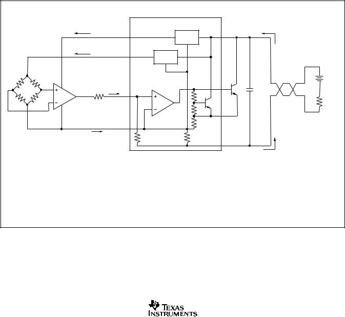
The XTR115 and XTR116 are identical devices except for the reference voltage output, pin 1. This voltage is available for external circuitry and is not used internally. Further discussions that apply to both devices will refer to the “XTR115/6.”
Figure 1 shows basic circuit connections with representative simplified input circuitry. The XTR115/6 is a two-wire current transmitter. Its input signal (pin 2) controls the output current. A portion of this current flows into the V+ power supply, pin 7. The remaining current flows in Q1. External input circuitry connected to the XTR115/6 can be powered from VREG or VREF. Current drawn from these terminals
must be returned to IRET, pin 3. This IRET pin is a “local ground” for input circuitry driving the XTR115/6.
The XTR115/6 is a current-input device with a gain of 100. A current flowing into pin 2 produces IO = 100 • IIN. The
input voltage at the IIN pin is zero (referred to the IRET pin). A voltage input is created with an external input resistor, as
shown. Common full-scale input voltages range from 1V
and upward. Full-scale inputs greater than 0.5V are recommend to minimize the effect of offset voltage and drift of A1.
EXTERNAL TRANSISTOR
The external transistor, Q1, conducts the majority of the fullscale output current. Power dissipation in this transistor can approach 0.8W with high loop voltage (40V) and 20mA output current. The XTR115/6 is designed to use an external transistor to avoid on-chip thermal-induced errors. Heat produced by Q1 will still cause ambient temperature changes that can affect the XTR115/6. To minimize these effects, locate Q1 away from sensitive analog circuitry, including XTR115/6. Mount Q1 so that heat is conducted to the outside of the transducer housing.
The XTR115/6 is designed to use virtually any NPN transistor with sufficient voltage, current and power rating. Case style and thermal mounting considerations often influence the choice for any given application. Several possible choices are listed in Figure 1. A MOSFET transistor will not improve the accuracy of the XTR115/6 and is not recommended.
|
|
|
|
XTR115 |
|
|
|
|
|
IREG |
|
|
XTR116 |
|
|
|
IO |
|
5V |
VREG |
|
+5V |
V+ |
|
||
XTR115: 2.5V |
|
|
|
|
||||
|
|
8 |
|
Regulator |
7 |
|
|
|
XTR116: 4.096V |
|
|
|
|
|
|||
|
|
|
|
|
|
|
|
|
|
IREF |
|
(1) |
Voltage |
|
|
|
|
|
|
|
VREF |
|
|
|
|
|
|
|
|
1 |
Reference |
|
|
|
|
|
RIN |
|
|
|
|
|
|
VLOOP |
|
IIN |
|
|
|
B |
Q1 |
10nF |
|
Input |
20kΩ |
IIN |
|
|
6 |
|||
VIN |
|
|
|
|
|
|||
Circuitry |
|
|
2 |
|
|
|
|
RL |
|
|
|
A1 |
|
|
|
||
|
|
|
|
|
|
|
||
|
|
|
|
|
|
E |
|
|
|
|
|
|
|
|
5 |
|
|
|
|
|
3 |
|
|
RLIM |
|
|
|
All return current |
IRET |
R1 |
R2 |
|
|
|
|
|
from IREG and IREF |
|
2.475kΩ |
25Ω |
I |
|
|
|
|
|
|
|
|
|
O |
|
|
|
|
|
|
|
|
4 |
|
I = 100 • IIN |
For IO = 4mA to 20mA |
|
|
|
|
|
|
||
IIN = 40µ A to 200µ A |
|
|
|
|
|
|
|
|
With RIN = 20kΩ |
NOTE: (1) See also Figure 5. |
|
|
|
|
|||
VIN = 0.8V to 4V |
|
|
|
|
|
|
Possible choices for Q1 (see text). |
|
|
|
|
|
|
|
|
|
|
TYPE |
PACKAGE |
2N4922 |
TO-225 |
TIP29C |
TO-220 |
TIP31B |
TO-220 |
|
|
FIGURE 1. Basic Circuit Connections.
XTR115, XTR116 |
5 |
|
SBOS124A |
www.ti.com |
 Loading...