


XTR105
–200°C
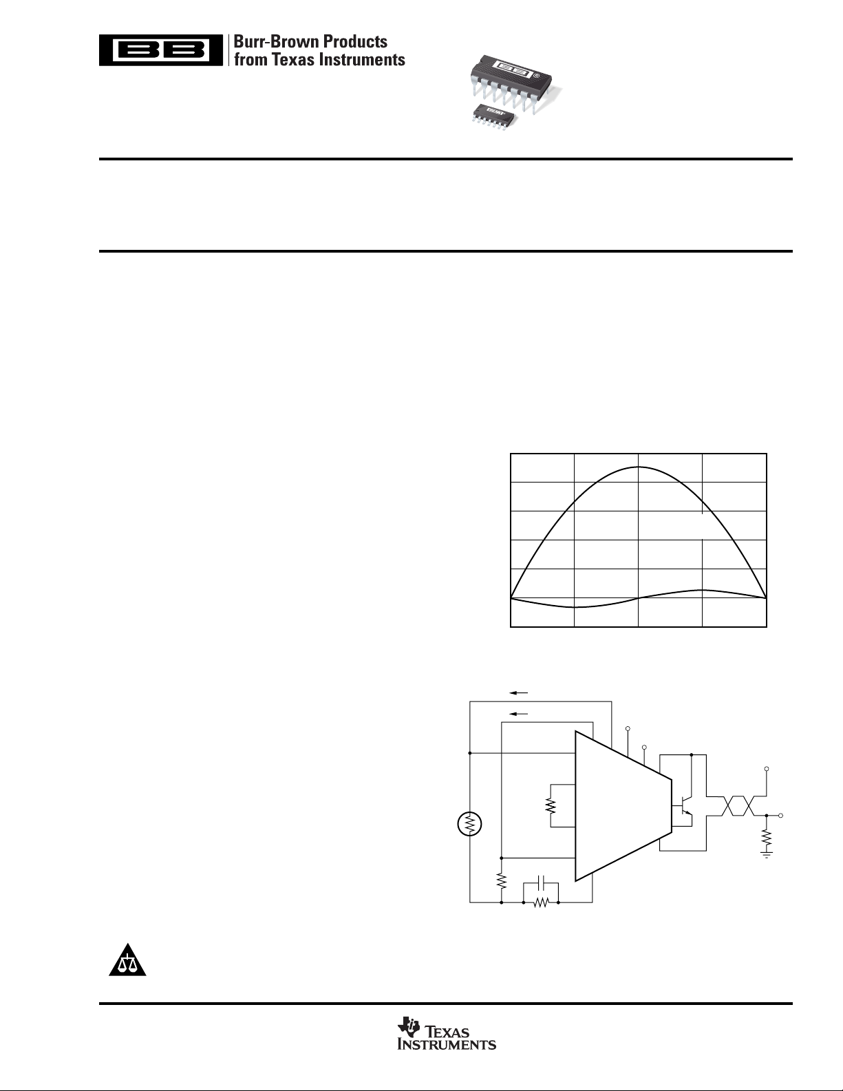
Pt100 NONLINEARITY CORRECTION
USING XTR105
Process Temperature (°C)
+850°C
5
4
3
2
1
0
–1
Uncorrected
RTD Nonlinearity
Corrected
Nonlinearity
Nonlinearity (%)
XTR105
XTR105
XTR105
SBOS061B – FEBRUARY 1997 – REVISED AUGUST 2004
4-20mA CURRENT TRANSMITTER
with Sensor Excitation and Linearization
FEATURES
● LOW UNADJUSTED ERROR
● TWO PRECISION CURRENT SOURCES: 800µA each
● LINEARIZATION
● 2- OR 3-WIRE RTD OPERATION
● LOW OFFSET DRIFT: 0.4µV/°C
● LOW OUTPUT CURRENT NOISE: 30nA
PP
APPLICATIONS
● INDUSTRIAL PROCESS CONTROL
● FACTORY AUTOMATION
● SCADA REMOTE DATA ACQUISITION
● REMOTE TEMPERATURE AND PRESSURE
TRANSDUCERS
● HIGH PSR: 110dB minimum
● HIGH CMR: 86dB minimum
● WIDE SUPPLY RANGE: 7.5V to 36V
● DIP-14 AND SO-14 PACKAGES
DESCRIPTION
The XTR105 is a monolithic 4-20mA, 2-wire current transmitter with two precision current sources. It provides complete
current excitation for platinum RTD temperature sensors and
bridges, instrumentation amplifiers, and current output circuitry on a single integrated circuit.
Versatile linearization circuitry provides a 2nd-order correction to the RTD, typically achieving a 40:1 improvement in
linearity.
Instrumentation amplifier gain can be configured for a wide
range of temperature or pressure measurements. Total unadjusted error of the complete current transmitter is low
enough to permit use without adjustment in many applications. This includes zero output current drift, span drift, and
nonlinearity. The XTR105 operates on loop power-supply
voltages down to 7.5V.
RTD
The XTR105 is available in DIP-14 and SO-14 surfacemount packages and is specified for the –40°C to +85°C
industrial temperature range.
= 0.8mA
I
R
IR = 0.8mA
R
G
+
–
V
LIN
XTR105
V
REG
7.5V to 36V
4-20 mA
V
PS
V
O
R
L
Please be aware that an important notice concerning availability, standard warranty, and use in critical applications of
Texas Instruments semiconductor products and disclaimers thereto appears at the end of this data sheet.
All trademarks are the property of their respective owners.
PRODUCTION DATA information is current as of publication date.
Products conform to specifications per the terms of Texas Instruments
standard warranty. Production processing does not necessarily include
testing of all parameters.
Copyright © 1997-2004, Texas Instruments Incorporated
www.ti.com
ABSOLUTE MAXIMUM RATINGS
(1)
Power Supply, V+ (referenced to the IO pin)...................................... 40V
, V
Input Voltage, V
(referenced to the IO pin) ....................0V to V+
IN+
IN–
Storage Temperature Range ......................................... –55°C to +125°C
Lead Temperature (soldering, 10s) ............................................... +300°C
Output Current Limit ................................................................ Continuous
Junction Temperature .................................................................... +165°C
NOTE: (1) Stresses above those listed under “Absolute Maximum Ratings”
may cause permanent damage to the device. Exposure to absolute maximum
conditions for extended periods may affect device reliability.
ELECTROSTATIC
DISCHARGE SENSITIVITY
This integrated circuit can be damaged by ESD. Texas Instruments recommends that all integrated circuits be handled with
appropriate precautions. Failure to observe proper handling
and installation procedures can cause damage.
ESD damage can range from subtle performance degradation to complete device failure. Precision integrated circuits
may be more susceptible to damage because very small
parametric changes could cause the device not to meet its
published specifications.
PACKAGE/ORDERING INFORMATION
(1)
SPECIFIED
PACKAGE TEMPERATURE PACKAGE ORDERING TRANSPORT
PRODUCT PACKAGE-LEAD DESIGNATOR RANGE MARKING NUMBER MEDIA, QUANTITY
XTR105 DIP-14 N –40°C to +85°C XTR105PA XTR105PA Rails, 25
" """XTR105P XTR105P Rails, 25
XTR105 SO-14 Surface-Mount D –40°C to +85°C XTR105UA XTR105UA Rails, 58
" """XTR105UA XTR105UA/2K5 Tape and Reel, 2500
XTR105 SO-14 Surface-Mount D –40°C to +85°C XTR105U XTR105U Rails, 58
" """XTR105U XTR105U/2K5 Tape and Reel, 2500
NOTE: (1) For the most current package and ordering information, see the Package Option Addendum located at the end of this data sheet.
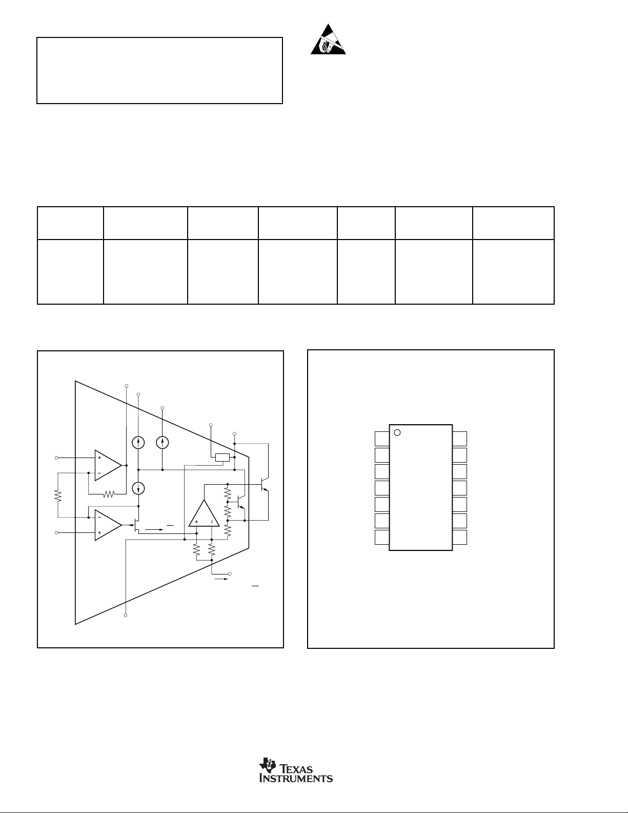
FUNCTIONAL BLOCK DIAGRAM
V
LIN
I
R1
12
13
+
V
IN
4
R
LIN
R
G
3
2
–
V
IN
1kΩ
6
I
RET
I
R2
1
14
800µA 800µA
100µA
V
I = 100µA +
R
IN
G
975Ω
V
REG
11
5.1V
25Ω
7
IO = 4mA + V
V+
10
B
Q
1
9
E
8
40
•
( )
IN
R
G
PIN CONFIGURATION
Top View DIP and SO
1
I
R1
– +
2
VIN
3
R
G
4
R
G
5
NC
6
I
RET
7
I
O
NC = No Internal Connection
14
13
12
11
10
9
8
I
R2
V
IN
V
LIN
V
REG
V+
B (Base)
E (Emitter)
2
www.ti.com
XTR105
SBOS061B

ELECTRICAL CHARACTERISTICS
At TA = +25°C, V+ = 24V, and TIP29C external transistor, unless otherwise noted.
XTR105P, U XTR105PA, UA
PARAMETER CONDITIONS MIN TYP MAX MIN TYP MAX UNITS
OUTPUT
Output Current Equation A
Output Current, Specified Range 4 20 ✻✻mA
Over-Scale Limit 24 27 30 ✻✻✻ mA
Under-Scale Limit I
ZERO OUTPUT
(1)
= 0V 1.8 2.2 2.6 ✻✻✻ mA
REG
VIN = 0V, RG = ∞ 4 ✻ mA
Initial Error ±5 ±25 ✻ ±50 µA
vs Temperature ±0.07 ±0.5 ✻ ±0.9 µA/°C
vs Supply Voltage, V+ V+ = 7.5V to 36V 0.04 0.2 ✻✻ µA/V
vs Common-Mode Voltage
vs V
Output Current 0.3 ✻ µA/mA
REG
Noise, 0.1Hz to 10Hz 0.03 ✻ µA
VCM = 1.25V to 3.5V
(2)
SPAN
Span Equation (transconductance)
Initial Error
vs Temperature
Nonlinearity, Ideal Input
INPUT
(3)
(3)
(4)
(5)
Full-Scale (VIN) = 50mV ±0.05 ±0.2 ✻ ±0.4 %
Full-Scale (VIN) = 50mV 0.003 0.01 ✻✻ %
Offset Voltage VCM = 2V ±50 ±100 ✻ ±250 µV
vs Temperature ±0.4 ±1.5 ✻ ±3 µV/°C
vs Supply Voltage, V+ V+ = 7.5V to 36V ±0.3 ±3 ✻✻ µV/V
vs Common-Mode Voltage, VCM = 1.25V to 3.5V
RTI (CMRR)
Common-Mode Input Range
(2)
(2)
Input Bias Current 525 ✻ 50 nA
vs Temperature 20 ✻ pA/°C
Input Offset Current ±0.2 ±3 ✻ ±10 nA
vs Temperature 5 ✻ pA/°C
Impedance, Differential 0.1 || 1 ✻ GΩ || pF
Common-Mode 5 || 10 ✻ GΩ || pF
Noise, 0.1Hz to 10Hz 0.6 ✻ µV
CURRENT SOURCES VO = 2V
(6)
Current 800 ✻ µA
Accuracy ±0.05 ±0.2 ✻ ±0.4 %
vs Temperature ±15 ±35 ✻ ±75 ppm/°C
vs Power Supply, V+ V+ = 7.5V to 36V ±10 ±25 ✻✻ ppm/V
Matching ±0.02 ±0.1 ✻ ±0.2 %
vs Temperature ±3 ±15 ✻ ±30 ppm/°C
vs Power Supply, V+ V+ = 7.5V to 36V 1 10 ✻✻ ppm/V
Compliance Voltage, Positive (V+) – 3
Negative
(2)
Output Impedance 150 ✻ MΩ
Noise, 0.1Hz to 10Hz 0.003 ✻ µA
(2)
V
REG
Accuracy ±0.02 ±0.1 ✻✻ V
vs Temperature ±0.2 ✻ mV/°C
vs Supply Voltage, V+ 1 ✻ mV/V
Output Current ±1 ✻ mA
Output Impedance 75 ✻ Ω
LINEARIZATION
R
(internal) 1 ✻ kΩ
LIN
Accuracy ±0.2 ±0.5 ✻ ±1%
vs Temperature ±25 ±100 ✻✻ ppm/°C
POWER SUPPLY
Specified +24 ✻ V
Voltage Range +7.5 +36 ✻✻V
TEMPERATURE RANGE
Specification, T
Operating –55 +125 ✻✻°C
MIN
to T
MAX
Storage –55 +125 ✻✻°C
Thermal Resistance,
DIP-14 80 ✻ °C/W
θ
JA
SO-14 Surface-Mount 100 ✻ °C/W
✻ Specification same as XTR105P and XTR105U.
NOTES: (1) Describes accuracy of the 4mA low-scale offset current. Does not include input amplifier effects. Can be trimmed to zero.
(2) Voltage measured with respect to I
(3) Does not include initial error or TCR of gain-setting resistor, R
RET
pin.
(4) Increasing the full-scale input range improves nonlinearity.
(5) Does not include Zero Output initial error.
(6) Current source output voltage with respect to I
RET
pin.
IO = VIN • (40/RG) + 4mA, VIN in Volts, RG in Ω
0.02 ✻ µA/V
S = 40/R
G
✻ A/V
±3 ±25 ✻✻ ppm/°C
±10 ±50 ✻ ±100 µV/V
1.25 3.5 ✻✻V
(V+) – 2.5
✻✻ V
0 –0.2 ✻✻ V
5.1 ✻ V
–40 +85 ✻✻°C
.
G
PP
PP
PP
XTR105
SBOS061B
www.ti.com
3
TYPICAL CHARACTERISTICS
At TA = +25°C and V+ = 24V, unless otherwise noted.
50
40
30
20
10
Transconductance (20 Log mA/V)
0
100 1k 10k 100k
110
100
90
80
70
60
50
40
Common-Mode Rejection (dB)
30
20
TRANSCONDUCTANCE vs FREQUENCY
RG = 500Ω
RG = 2kΩ
Frequency (Hz)
COMMON-MODE REJECTION vs FREQUENCY
Full-Scale Input = 50mV
RG = 2kΩ
10 100 1k 10k 100k
Frequency (Hz)
R
G
= 125Ω
RG = 125Ω
1M
1M
STEP RESPONSE
RG = 2kΩ
20mA
RG = 125Ω
4mA/div
4mA
25µs/div
140
120
100
80
60
40
Power Supply Rejection (dB)
20
POWER-SUPPLY REJECTION vs FREQUENCY
RG = 2kΩ
0
10 100 1k 10k 100k
Frequency (Hz)
RG = 125Ω
1M
29
28
27
V+ = 36V
26
25
Over-Scale Current (mA)
24
23
–75 –50 –25 0 25 50 75 100
4
OVER-SCALE CURRENT vs TEMPERATURE
With External Transistor
V+ = 7.5V
V+ = 24V
Temperature (°C)
125
www.ti.com
2.40
2.35
2.30
2.25
Under-Scale Current (mA)
2.20
2.15
UNDER-SCALE CURRENT vs TEMPERATURE
V+ = 7.5V to 36V
–75 –50 –25 0 25 50 75 100
Temperature (°C)
125
XTR105
SBOS061B
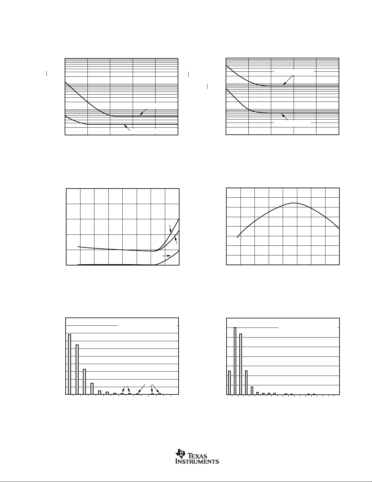
TYPICAL CHARACTERISTICS (Cont.)
–75 –50 –25 0 25 50 75 100
Temperature (°C)
ZERO OUTPUT CURRENT ERROR
vs TEMPERATURE
125
4
2
0
–2
–4
–6
–8
–10
–12
Zero Output Current Error (µA)
At TA = +25°C and V+ = 24V, unless otherwise noted.
INPUT VOLTAGE AND CURRENT
NOISE DENSITY vs FREQUENCY
10k
1k
100
Input Voltage Noise (nV/√Hz)
10
1 10 100 1k 10k
Frequency (Hz)
INPUT BIAS AND OFFSET CURRENT
vs TEMPERATURE
25
20
15
Current Noise
Voltage Noise
ZERO OUTPUT AND REFERENCE
10k
1k
100
Input Current Noise (fA/√Hz)
10
100k
+I
B
10k
1k
100
Noise (pA/√Hz)
10
1 10 100 1k 10k
CURRENT NOISE vs FREQUENCY
Zero Output Current
Reference Current
100k
Frequency (Hz)
10
5
Input Bias and Offset Current (nA)
0
–75 –50 –25 0 25 50 75 100
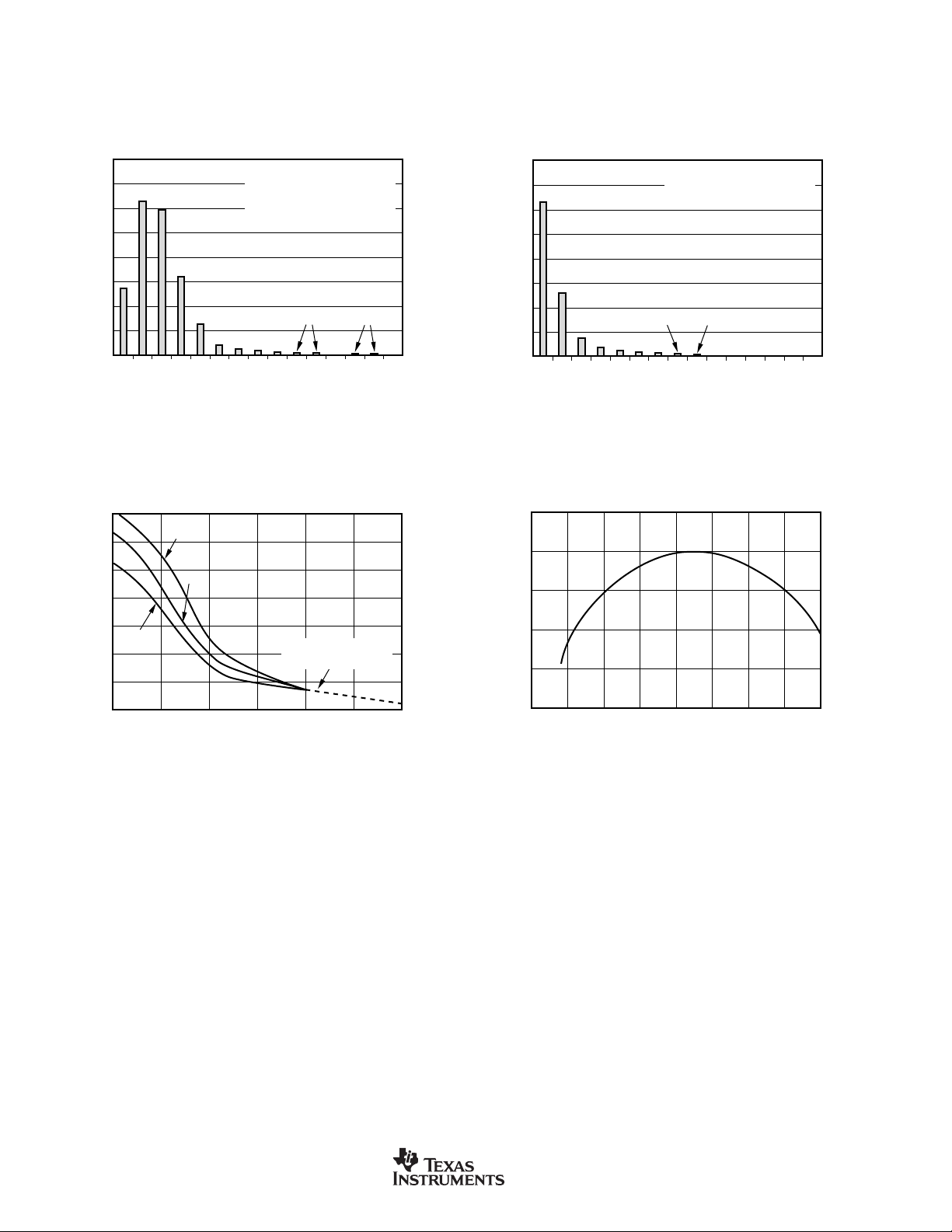
INPUT OFFSET VOLTAGE DRIFT
50
45
40
35
30
25
20
15
Percent of Units (%)
10
5
0
0.2
XTR105
SBOS061B
PRODUCTION DISTRIBUTION
0.4
0.6
0.8
Input Offset Voltage Drift (µV/°C)
Temperature (°C)
Typical Production Distribution
0.1%
1.0
1.2
1.4
1.6
1.8
I
OS
of Packaged Units.
0.02%
2.0
2.2
2.4
2.6
2.8
–I
B
125
3.0
www.ti.com
40
35
30
25
20
15
Percent of Units (%)
10
5
0
0.025
0.050
0.075
ZERO OUTPUT DRIFT
PRODUCTION DISTRIBUTION
Typical Production Distribution
0.100
0.125
0.150
0.175
0.200
0.225
0.250
0.275
0.300
Zero Output Drift (µA/°C)
of Packaged Units.
0.325
0.350
0.375
0.400
0.425
0.450
0.475
0.500
5
TYPICAL CHARACTERISTICS (Cont.)
At TA = +25°C and V+ = 24V, unless otherwise noted.
40
35
30
25
20
15
Percent of Units (%)
10
5
0
5
10152025303540455055606570
OUTPUT VOLTAGE vs V
V
REG
5.35
5.30
5.25
5.20
125°C
CURRENT SOURCE DRIFT
PRODUCTION DISTRIBUTION
Typical Production Distribution
Current Source Drift (ppm/°C)
25°C
of Packaged Units.
I
AND IR2 Included.
R1
0.04%
OUTPUT CURRENT
REG
0.01%
CURRENT SOURCE MATCHING
80
70
60
50
40
30
Percent of Units (%)
20
10
0
75
+0.05
0
–0.05
DRIFT PRODUCTION DISTRIBUTION
Typical Production Distribution
0.07%
2
4
6
8
1012141618202224262830
Current Source Matching Drift (ppm/°C)
REFERENCE CURRENT ERROR
vs TEMPERATURE
of Packaged Units.
0.02%
5.15
Output Voltage (V)
REG
V
–55°C
5.10
5.05
5.00
–1.0 –0.5 0 0.5 1.0 1.5
Output Current (mA)
V
REG
NOTE: Above 1mA,
Zero Output Degrades
2.0
–0.10
–0.15
Reference Current Error (%)
–0.20
–75 –50 –25 0 25 50 75 100 125
Temperature (°C)
6
www.ti.com
XTR105
SBOS061B
 Loading...