


A723
PRECISION VOLTAGE REGULATORS
SLVS057D ± AUGUST 1972 ± REVISED JULY 1999
D 150-mA Load Current Without External |
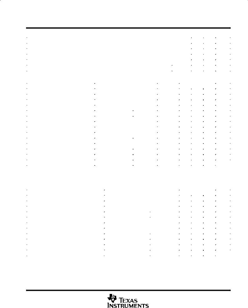
D OR N PACKAGE |
|||||
Power Transistor |
|
(TOP VIEW) |
|
|
||
D Adjustable Current-Limiting Capability |
NC |
|
|
|
|
NC |
|
1 |
14 |
|
|||
|
|
|||||
D Input Voltages up to 40 V |
|
|
||||
CURR LIM |
|
2 |
13 |
|
FREQ COMP |
|
|
|
|||||
D Output Adjustable From 2 V to 37 V |
|
|
||||
CURR SENS |
|
3 |
12 |
|
VCC+ |
|
|
|
|||||
|
IN± |
|
|
|||
D Direct Replacement for Fairchild A723C |
|
4 |
11 |
|
VC |
|
|
|
|||||
description |
IN+ |
|
5 |
10 |
|
OUTPUT |
REF |
|
6 |
9 |
|
VZ |
|
|
|
|||||
|
|
|||||
The A723 is a precision integrated-circuit |
VCC± |
|
7 |
8 |
|
NC |
|
|
|||||
|
|
|
|
|
|
|
voltage regulator, featuring high ripple rejection, |
|
|
|
|
|
|
excellent input and load regulation, excellent temperature stability, and low standby current. The circuit consists of a temperature-compensated reference-voltage amplifier, an error amplifier, a 150-mA output transistor, and an adjustable-output current limiter.
The A723 is designed for use in positive or negative power supplies as a series, shunt, switching, or floating regulator. For output currents exceeding 150 mA, additional pass elements can be connected as shown in Figures 4 and 5.
The A723C is characterized for operation from 0°C to 70°C.
AVAILABLE OPTIONS
|
PACKAGED DEVICES |
CHIP |
||
|
|
|
||
|
PLASTIC |
SMALL |
||
TA |
FORM |
|||
DIP |
OUTLINE |
|||
|
(Y) |
|||
|
(N) |
(D) |
||
|
|
|||
|
|
|
|
|
0°C to 70°C |
A723CN |
A723CD |
A723Y |
|
|
|
|
|
|
The D package is available taped and reeled. Add the suffix R to the device type (e.g., A723CDR). Chip forms are tested at 25°C.
functional block diagram |
|
|
|
|
|
|
|
VCC+ |
FREQ COMP |
|
|
|
|
|
|
||
Temperature- |
|
|
|
VC |
|
Compensated |
|
|
|
||
|
IN± |
± |
Series Pass |
||
Reference Diode |
|
||||
Ref |
REF |
Error |
Transistor |
||
|
|||||
|
Amp |
Amp |
|
||
|
|
|
|||
Current |
|
IN+ |
+ |
|
|
|
|
Current |
Regulated |
||
Source |
|
|
Limiter |
Output |
VCC± |
CURR LIM CURR SENS |
V |
|
|
Z |
Please be aware that an important notice concerning availability, standard warranty, and use in critical applications of Texas Instruments semiconductor products and disclaimers thereto appears at the end of this data sheet.
PRODUCTION DATA information is current as of publication date. Products conform to specifications per the terms of Texas Instruments standard warranty. Production processing does not necessarily include testing of all parameters.
Copyright 1999, Texas Instruments Incorporated
POST OFFICE BOX 655303 •DALLAS, TEXAS 75265 |
1 |

A723
PRECISION VOLTAGE REGULATORS
SLVS057D ± AUGUST 1972 ± REVISED JULY 1999
schematic
VCC+ VC
500 Ω |
25 kΩ |
1 kΩ |
1 kΩ |
|
15 kΩ
|
|
|
15 kΩ |
OUTPUT |
|
|
|
|
|
|
|
|
|
6.2 V |
100 Ω |
|
|
|
VZ |
|
|
|
|
|
5 pF |
|
|
|
|
30 kΩ |
|
|
|
FREQ COMP |
|
|
|
|
|
5 kΩ |
300 Ω 20 kΩ |
150 Ω |
|
CURR LIM |
|
|
|
|
CURR SENS |
REF |
IN+ |
VCC± |
IN± |
|
Resistor and capacitor values shown are nominal.
absolute maximum ratings over operating free-air temperature range (unless otherwise noted)²
Peak voltage from VCC+ to VCC± (tw ≤ 50 ms) . . . . . . . . . . . . . . . . . . . . . . . . . . . . . . . . . . . . . . . . |
. . . . . . . . . 50 |
V |
Continuous voltage from VCC+ to VCC± . . . . . . . . . . . . . . . . . . . . . . . . . . . . . . . . . . . . . . . . . . . . . . |
. . . . . . . . . 40 |
V |
Input-to-output voltage differential . . . . . . . . . . . . . . . . . . . . . . . . . . . . . . . . . . . . . . . . . . . . . . . . . . . |
. . . . . . . . . 40 |
V |
Differential input voltage to error amplifier . . . . . . . . . . . . . . . . . . . . . . . . . . . . . . . . . . . . . . . . . . . . |
. . . . . . . . . ±5 V |
|
Voltage between noninverting input and VCC± . . . . . . . . . . . . . . . . . . . . . . . . . . . . . . . . . . . . . . . . |
. . . . . . . . . . 8 |
V |
Current from VZ . . . . . . . . . . . . . . . . . . . . . . . . . . . . . . . . . . . . . . . . . . . . . . . . . . . . . . . . . . . . . . . . . . |
. . . . . . . 25 mA |
|
Current from REF . . . . . . . . . . . . . . . . . . . . . . . . . . . . . . . . . . . . . . . . . . . . . . . . . . . . . . . . . . . . . . . . . |
. . . . . . . 15 mA |
|
Package thermal impedance, θJA (see Notes 1 and 2): D package . . . . . . . . . . . . . . . . . . . . . . |
. . . . . . 86°C/W |
|
N package . . . . . . . . . . . . . . . . . . . . . . |
. . . . . 101°C/W |
|
Lead temperature 1,6 mm (1/16 inch) from case for 10 seconds: D or N package . . . . . . . . . |
. . . . . . . 260°C |
|
Storage temperature range, Tstg . . . . . . . . . . . . . . . . . . . . . . . . . . . . . . . . . . . . . . . . . . . . . . . . . . . |
±65°C to 150°C |
|
²Stresses beyond those listed under ªabsolute maximum ratingsº may cause permanent damage to the device. These are stress ratings only, and functional operation of the device at these or any other conditions beyond those indicated under ªrecommended operating conditionsº is not implied. Exposure to absolute-maximum-rated conditions for extended periods may affect device reliability.
NOTES: 1. Maximum power dissipation is a function of TJ(max), θJA, and TA. The maximum allowable power dissipation at any allowable ambient temperature is PD = (TJ(max) ± TA)/θJA. Operating at the absolute maximum TJ of 150°C can impact reliability.
2.The package thermal impedance is calculated in accordance with JESD 51, except for through-hole packages, which use a trace length of zero.
2 |
POST OFFICE BOX 655303 •DALLAS, TEXAS 75265 |
A723
PRECISION VOLTAGE REGULATORS
SLVS057D ± AUGUST 1972 ± REVISED JULY 1999
recommended operating conditions
|
|
MIN |
MAX |
UNIT |
|
|
|
|
|
Input voltage, VI |
|
9.5 |
40 |
V |
Output voltage, VO |
|
2 |
37 |
V |
Input-to-output voltage differential, VC ± VO |
|
3 |
38 |
V |
Output current, IO |
|
|
150 |
mA |
Operating free-air temperature range, TA |
µA723C |
0 |
70 |
°C |
electrical characteristics at specified free-air temperature (see Notes 3 and 4)
PARAMETER |
TEST CONDITIONS |
TA |
|
µA723C |
|
UNIT |
||
|
|
|
||||||
MIN |
TYP |
MAX |
||||||
|
|
|
|
|
||||
|
|
|
|
|
|
|
|
|
|
VI = 12 V to VI = 15 V |
|
25°C |
|
0.1 |
1 |
|
|
Input regulation |
VI = 12 V to VI = 40 V |
|
25°C |
|
1 |
5 |
mV/V |
|
|
VI = 12 V to VI = 15 V |
|
0°C to 70°C |
|
|
3 |
|
|
Ripple rejection |
f = 50 Hz to 10 kHz, |
Cref = 0 |
25°C |
|
74 |
|
dB |
|
f = 50 Hz to 10 kHz, |
Cref = 5 µF |
25°C |
|
86 |
|
|||
|
|
|
|
|||||
Output regulation |
|
|
25°C |
|
±0.3 |
±2 |
mV/V |
|
|
|
|
|
|
|
|||
|
|
0°C to 70°C |
|
|
±6 |
|||
|
|
|
|
|
|
|||
Reference voltage, Vref |
|
|
25°C |
6.8 |
7.15 |
7.5 |
V |
|
Standby current |
VI = 30 V, |
IO = 0 |
25°C |
|
2.3 |
4 |
mA |
|
Temperature coefficient of output voltage |
|
|
0°C to 70°C |
|
0.003 |
0.015 |
%/°C |
|
Short-circuit output current |
RSC = 10 Ω, |
VO = 0 |
25°C |
|
65 |
|
mA |
|
Output noise voltage |
BW = 100 Hz to 10 kHz, |
Cref = 0 |
25°C |
|
20 |
|
µV |
|
BW = 100 Hz to 10 kHz, |
Cref = 5 µF |
25°C |
|
2.5 |
|
|||
|
|
|
|
|||||
NOTES: 3. For all values in this table, the device is connected as shown in Figure 1 with the divider resistance as seen by the error amplifier
≤10 kΩ. Unless otherwise specified, VI = VCC+ = VC = 12 V, VCC± = 0, VO = 5 V, IO = 1 mA, RSC = 0, and Cref = 0.
4.Pulse-testing techniques must be used that will maintain the junction temperature as close to the ambient temperature as possible.
electrical characteristics, TA = 25°C (see Notes 3 and 4)
PARAMETER |
TEST CONDITIONS |
|
µA723Y |
|
UNIT |
||
|
|
|
|||||
MIN |
TYP |
MAX |
|||||
|
|
|
|
||||
|
|
|
|
|
|
|
|
Input regulation |
VI = 12 V to VI = 15 V |
|
|
0.1 |
|
mV/V |
|
VI = 12 V to VI = 40 V |
|
|
1 |
|
|||
|
|
|
|
|
|||
Ripple rejection |
f = 50 Hz to 10 kHz, |
Cref = 0 |
|
74 |
|
dB |
|
f = 50 Hz to 10 kHz, |
Cref = 5 µF |
|
86 |
|
|||
|
|
|
|
||||
Output regulation |
|
|
|
±0.3 |
|
mV/V |
|
|
|
|
|
|
|
|
|
Reference voltage, Vref |
|
|
|
7.15 |
|
V |
|
Standby current |
VI = 30 V, |
IO = 0 |
|
2.3 |
|
mA |
|
Short-circuit output current |
RSC = 10 Ω, |
VO = 0 |
|
65 |
|
mA |
|
Output noise voltage |
BW = 100 Hz to 10 kHz, |
Cref = 0 |
|
20 |
|
µV |
|
BW = 100 Hz to 10 kHz, |
Cref = 5 µF |
|
2.5 |
|
|||
|
|
|
|
||||
NOTES: 3. For all values in this table, the device is connected as shown in Figure 1 with the divider resistance as seen by the error amplifier
≤10 kΩ. Unless otherwise specified, VI = VCC+ = VC = 12 V, VCC± = 0, VO = 5 V, IO = 1 mA, RSC = 0, and Cref = 0.
4.Pulse-testing techniques must be used that will maintain the junction temperature as close to the ambient temperature as possible.
POST OFFICE BOX 655303 •DALLAS, TEXAS 75265 |
3 |
A723
PRECISION VOLTAGE REGULATORS
SLVS057D ± AUGUST 1972 ± REVISED JULY 1999
APPLICATION INFORMATION
Table 1. Resistor Values (kΩ) for Standard Output Voltages
|
|
FIXED OUTPUT |
OUTPUT ADJUSTABLE |
||||||
OUTPUT |
APPLICABLE |
|
±10% |
|
|
||||
|
±5% |
|
|
|
|||||
|
|
(SEE NOTE 6) |
|
||||||
VOLTAGE |
FIGURES |
|
|
|
|
|
|||
|
|
|
|
|
|
|
|
||
(V) |
(SEE NOTE 5) |
R1 |
|
R2 |
R1 |
|
P1 |
|
P2 |
|
|
(kΩ) |
|
(kΩ) |
(kΩ) |
|
(kΩ ) |
|
(kΩ ) |
|
|
|
|
|
|
|
|
|
|
3.0 |
1, 5, 6, 9, 11, 12 (4) |
4.12 |
|
3.01 |
1.8 |
|
0.5 |
|
1.2 |
3.6 |
1, 5, 6, 9, 11, 12 (4) |
3.57 |
|
3.65 |
1.5 |
|
0.5 |
|
1.5 |
5.0 |
1, 5, 6, 9, 11, 12 (4) |
2.15 |
|
4.99 |
0.75 |
|
0.5 |
|
2.2 |
6.0 |
1, 5, 6, 9, 11, 12 (4) |
1.15 |
|
6.04 |
0.5 |
|
0.5 |
|
2.7 |
9.0 |
2, 4, (5, 6, 9, 12) |
1.87 |
|
7.15 |
0.75 |
|
1.0 |
|
2.7 |
12 |
2, 4, (5, 6, 9, 12) |
4.87 |
|
7.15 |
2.0 |
|
1.0 |
|
3.0 |
15 |
2, 4, (5, 6, 9, 12) |
7.87 |
|
7.15 |
3.3 |
|
1.0 |
|
3.0 |
28 |
2, 4, (5, 6, 9, 12) |
21.0 |
|
7.15 |
5.6 |
|
1.0 |
|
2.0 |
45 |
7 |
3.57 |
|
48.7 |
2.2 |
|
10 |
|
39 |
75 |
7 |
3.57 |
|
78.7 |
2.2 |
|
10 |
|
68 |
100 |
7 |
3.57 |
|
105 |
2.2 |
|
10 |
|
91 |
250 |
7 |
3.57 |
|
255 |
2.2 |
|
10 |
|
240 |
±6 |
3, 10 |
3.57 |
|
2.43 |
1.2 |
|
0.5 |
|
0.75 |
(see Note 7) |
|
|
|
||||||
|
|
|
|
|
|
|
|
|
|
±9 |
3, 10 |
3.48 |
|
5.36 |
1.2 |
|
0.5 |
|
2.0 |
±12 |
3, 10 |
3.57 |
|
8.45 |
1.2 |
|
0.5 |
|
3.3 |
±15 |
3, 10 |
3.57 |
|
11.5 |
1.2 |
|
0.5 |
|
4.3 |
±28 |
3, 10 |
3.57 |
|
24.3 |
1.2 |
|
0.5 |
|
10 |
±45 |
8 |
3.57 |
|
41.2 |
2.2 |
|
10 |
|
33 |
±100 |
8 |
3.57 |
|
95.3 |
2.2 |
|
10 |
|
91 |
±250 |
8 |
3.57 |
|
249 |
2.2 |
|
10 |
|
240 |
|
|
|
|
|
|
|
|
|
|
NOTES: 5. The R1/R2 divider can be across either VO or V(ref). If the divider is across V(ref), use the figure numbers without parentheses. If the divider is across
VO, use the figure numbers in parentheses.
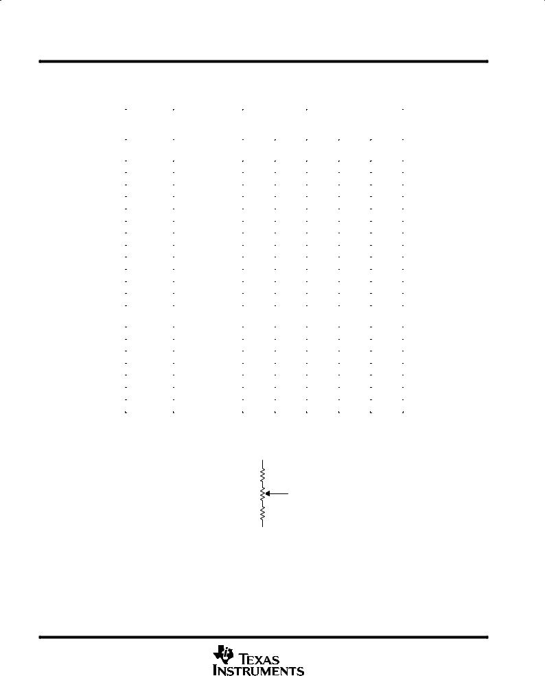
6.To make the voltage adjustable, the R1/R2 divider shown in the figures must be replaced by the divider shown below.
R1
P1
R2
Adjustable Output Circuit
7.For Figures 3, 8, and 10, the device requires a minimum of 9 V between VCC+ and VCC± when VO is equal to or more positive than ±9 V.
4 |
POST OFFICE BOX 655303 •DALLAS, TEXAS 75265 |
 Loading...