Texas Instruments uA709MW, uA709MU, uA709MJ, uA709MJG, uA709CP Datasheet
...
uA709C, uA709M, uA709AM GENERAL-PURPOSE OPERATIONAL AMPLIFIERS
SLOS096 ± D942, FEBRUARY 1971 ± REVISED MAY 1988
•Common-Mode Input Range . . . ± 10 V
Typical
•Designed to Be Interchangeable With Fairchild μA709A, μA709, and μA709C
•Maximum Peak-to-Peak Output Voltage Swing . . . 28-V Typical With 15-V Supplies
description
These circuits are general-purpose operational amplifiers, each having high-impedance differential inputs and a low-impedance output. Component matching, inherent with silicon monolithic circuit-fabrication techniques, produces an amplifier with low-drift and low-offset characteristics. Provisions are incorporated within the circuit whereby external components may be used to compensate the amplifier for stable operation under various feedback or load conditions. These amplifiers are particularly useful for applications requiring transfer or generation of linear or nonlinear functions.
The uA709A circuit features improved offset characteristics, reduced input-current requirements, and lower power dissipation when compared to the uA709 circuit. In addition, maximum values of the average temperature coefficients of offset voltage and current are specified for the uA709A.
The uA709C is characterized for operation from 0°C to 70°C. The uA709AM and uA709M are characterized for operation over the full military temperature range of ±55°C to 125°C.
uA709AM, uA709M . . . J OR W PACKAGE
(TOP VIEW)
NC |
|
1 |
14 |
|
NC |
|
|
||||
NC |
|
2 |
13 |
|
NC |
|
|
||||
FREQ COMP B |
|
3 |
12 |
|
FREQ COMP A |
|
|
||||
IN ± |
|
4 |
11 |
|
VCC + |
|
|
||||
IN + |
|
5 |
10 |
|
OUT |
|
|
||||
VCC ± |
|
6 |
9 |
|
OUT FREQ COMP |
|
|
||||
NC |
|
7 |
8 |
|
NC |
|
|
||||
|
|
|
|
|
|
uA709AM, uA709M . . . JG PACKAGE uA709C . . . D, JG, OR P PACKAGE (TOP VIEW)
FREQ COMP B |
|
1 |
8 |
|
|
FREQ COMP A |
|
|
|
|
|||||
IN ± |
|
2 |
7 |
|
|
VCC + |
|
|
|
|
|||||
IN + |
|
3 |
6 |
|
|
OUT |
|
|
|
|
|||||
VCC ± |
|
4 |
5 |
|
|
OUT FREQ COMP |
|
|
|
|
|||||
|
|
|
|
|
|
|
|
|
|
|
|
|
|
|
|
uA709AM, uA709M . . . U FLAT PACKAGE |
|||||||
|
|
(TOP VIEW) |
|
|
|||
NC |
|
|
|
|
|
NC |
|
|
1 |
10 |
|
|
|||
|
|
|
|||||
FREQ COMP B |
|
2 |
9 |
|
|
FREQ COMP A |
|
|
|
|
|||||
IN ± |
|
3 |
8 |
|
|
VCC + |
|
|
|
|
|||||
IN + |
|
4 |
7 |
|
|
OUT |
|
|
|
|
|||||
VCC |
|
5 |
6 |
|
|
OUT FREQ COMP |
|
|
|
|
|||||
|
|
|
|
|
|
|
|
NC ± No internal connection
symbol
|
|
OUT FREQ COMP |
|||||
IN + |
|
+ |
|
|
|
OUT |
|
|
|
|
|
||||
IN ± |
|
± |
|
|
|
||
|
|
|
|
||||
|
|
|
|
|
|||
|
|
|
|
|
|||
|
|
|
|
|
|
|
|
|
FREQ |
FREQ |
|||||
|
COMP COMP |
||||||
|
A |
|
B |
||||
AVAILABLE OPTIONS
|
VIO max |
|
|
PACKAGE |
|
|
||
TA |
|
|
|
|
|
|
||
SMALL OUTLINE |
CERAMIC |
CERAMIC DIP |
PLASTIC DIP |
FLAT PACK |
FLAT PACK |
|||
AT 25°C |
||||||||
|
(D) |
(J) |
(JG) |
(P) |
(U) |
(W) |
||
|
|
|||||||
|
|
|
|
|
|
|
|
|
0°C |
|
|
|
|
|
|
|
|
to |
7.5 mV |
uA709CD |
Ð |
uA709CJG |
uA709CP |
Ð |
Ð |
|
70°C |
|
|
|
|
|
|
|
|
|
|
|
|
|
|
|
|
|
± 55°C |
5 mV |
|
uA709MJ |
uA709MJG |
|
uA709MU |
uA709MW |
|
to |
|
Ð |
|
|
Ð |
|
|
|
125°C |
2 mV |
uA709AMJ |
uA709AMJG |
uA709AMU |
uA709AMW |
|||
|
|
|||||||
The D package is available taped and reeled. Add the suffix R to the device type when ordering, (e.g., uA709CDR).
PRODUCTION DATA information is current as of publication date. Products conform to specifications per the terms of Texas Instruments standard warranty. Production processing does not necessarily include testing of all parameters.
Copyright 1988, Texas Instruments Incorporated
POST OFFICE BOX 655303 •DALLAS, TEXAS 75265 |
1 |

uA709C, uA709M, uA709AM GENERAL-PURPOSE OPERATIONAL AMPLIFIERS
SLOS096 ± D942, FEBRUARY 1971 ± REVISED MAY 1988
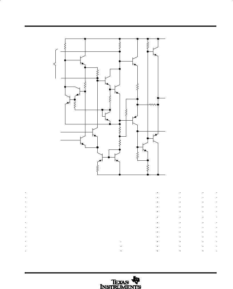
schematic
VCC +
10 kΩ |
10 kΩ |
20 kΩ |
|
A
FREQ
COMP
25 kΩ
 B
B
25 kΩ 1 kΩ
3 kΩ |
OUT |
3 kΩ |
30 kΩ |
|
|
|
10 kΩ |
3.6 kΩ |
OUT FREQ COMP |
IN ± |
IN + |
18 kΩ |
|
|
|
10 kΩ |
2.4 kΩ |
75 kΩ |
|
|
|
VCC ± |
Component values shown are nominal.
absolute maximum ratings over operating free-air temperature range (unless otherwise noted)
|
|
uA709C |
uA709M |
UNIT |
|
|
uA709AM |
||
|
|
|
|
|
|
|
|
|
|
Supply voltage, VCC + (see Note 1) |
|
18 |
18 |
V |
Supply voltage, VCC ± (see Note 1) |
|
± 18 |
± 18 |
V |
Differential input voltage (see Note 2) |
|
± 5 |
± 5 |
V |
|
|
|
|
|
Input voltage (either input, see Notes 1 and 3) |
|
± 10 |
± 10 |
V |
|
|
|
|
|
Duration of output short circuit (see Note 4) |
|
5 |
5 |
s |
|
|
|
|
|
Continuous total power dissipation |
|
See Dissipation Rating Table |
||
|
|
|
|
|
Operating free-air temperature range |
|
0 to 70 |
± 55 to 125 |
°C |
|
|
|
|
|
Storage temperature range |
|
± 65 to 150 |
± 65 to 150 |
°C |
|
|
|
|
|
Lead temperature 1,6 mm (1/16 inch) from case for 60 seconds |
J, JG, U, or W package |
300 |
300 |
°C |
|
|
|
|
|
Lead temperature 1,6 mm (1/16 inch) from case for 10 seconds |
D or P package |
260 |
|
°C |
NOTES: 1. All voltage values, unless otherwise noted, are with respect to the midpoint between VCC + and VCC ±.
2.Differential voltages are at the noninverting input terminal with respect to the inverting input terminal.
3.The magnitude of the input voltage must never exceed the magnitude of the supply voltage or 10 V, whichever is less.
4.The output may be shorted to ground or either power supply.
2 |
POST OFFICE BOX 655303 •DALLAS, TEXAS 75265 |
 Loading...