


 Loading...
Texas Instruments OPA2350EA, OPA350EA, OPA2350PA, OPA2350UA, OPA350PA Schematic [ru]
...Product |
Sample & |
Technical |
Tools & |
Support & |
|
|
Reference |
Folder |
Buy |
Documents |
Software |
Community |
|
|
Design |
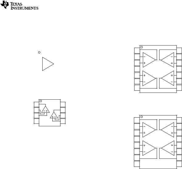
OPA350, OPA2350, OPA4350
SBOS099D –SEPTEMBER 2000 –REVISED DECEMBER 2015
OPAx350 High-Speed, Single-Supply, Rail-to-Rail Operational Amplifiers MicroAmplifier
Series
1 Features
•Rail-to-Rail Input
•Rail-to-Rail Output (Within 10 mV)
•Wide Bandwidth: 38 MHz
•High Slew Rate: 22 V/μs
•Low Noise: 5 nV/√Hz
•Low THD+Noise: 0.0006%
•Unity-Gain Stable
•MicroSize Packages
•Single, Dual, and Quad
2 Applications
•Cell Phone PA Control Loops
•Driving A/D Converters
•Video Processing
•Data Acquisition
•Process Controls
•Audio Processing
•Communications
•Active Filters
•Test Equipment
OPAx350 Harmonic Distortion
|
1 |
G = 1 |
|
|
|
(−40dBc) |
|
|
|
|
VO = 2.5VPP |
|
|
|
|
|
|
|
|
(%) |
0.1 |
RL = 600Ω |
|
|
|
|
|
||
(−60dBc) |
|
|
|
|
Distortion |
|
|
|
|
0.01 |
|
|
|
|
(−80dBc) |
|
|
|
|
Harmonic |
|
|
|
|
0.001 |
|
|
|
|
(−100dBc) |
|
|
|
|
|
3rd−Harmonic |
|
|
|
|
|
|
|
|
|
|
|
2nd−Harmonic |
|
|
0.0001 |
|
|
|
|
(−120dBc) 1k |
10k |
100k |
1M |
Frequency (Hz)
3 Description
The OPA350 series of rail-to-rail CMOS operational amplifiers are optimized for low voltage, single-supply operation. Rail-to-rail input and output, low noise (5 nV/√Hz), and high speed operation (38 MHz, 22 V/μs) make the amplifiers ideal for driving sampling Analog- to-Digital (A/D) converters. They are also suited for cell phone PA control loops and video processing (75-Ω drive capability), as well as audio and general purpose applications. Single, dual, and quad versions have identical specifications for maximum design flexibility.
The OPA350 series operates on a single supply as low as 2.5 V, with an input common-mode voltage range that extends 300 mV below ground and 300 mV above the positive supply. Output voltage swing is to within 10 mV of the supply rails, with a 10-kΩ load. Dual and quad designs feature completely independent circuitry for lowest crosstalk and freedom from interaction.
The single (OPA350) and dual (OPA2350) come in the miniature MSOP-8 surface mount, SO-8 surface mount, and DIP-8 packages. The quad (OPA4350) packages are in the space-saving SSOP-16 surface mount and SO-14 surface mount. All are specified from −40°C to 85°C and operate from −55°C to 150°C.
Device Information(1)
PART NUMBER |
PACKAGE |
BODY SIZE (NOM) |
|
|
MSOP (8) |
3.00 mm × 3.00 mm |
|
OPA350 |
SOIC (8) |
3.91 mm × 4.90 mm |
|
|
PDIP (8) |
6.35 mm × 9.81 mm |
|
|
MSOP (8) |
3.00 mm × 3.00 mm |
|
OPA2350 |
SOIC (8) |
3.91 mm × 4.90 mm |
|
|
PDIP (8) |
6.35 mm × 9.81 mm |
|
OPA4350 |
SSOP (16) |
3.90 mm × 4.90 mm |
|
SOIC (14) |
3.91 mm × 8.65 mm |
||
|
(1)For all available packages, see the orderable addendum at the end of the data sheet.
An IMPORTANT NOTICE at the end of this data sheet addresses availability, warranty, changes, use in safety-critical applications, intellectual property matters and other important disclaimers. PRODUCTION DATA.

OPA350, OPA2350, OPA4350
SBOS099D –SEPTEMBER 2000 –REVISED DECEMBER 2015 www.ti.com
Table of Contents
1 |
Features .................................................................. |
1 |
|
7.4 |
Device Functional Modes........................................ |
17 |
|
2 |
Applications ........................................................... |
1 |
8 |
Application and Implementation ........................ |
18 |
||
3 |
Description ............................................................. |
1 |
|
8.1 |
Application Information............................................ |
18 |
|
4 |
Revision History..................................................... |
2 |
|
8.2 |
Typical Applications ................................................ |
18 |
|
5 |
Pin Configuration and Functions ......................... |
3 |
9 |
Power Supply Recommendations...................... |
22 |
||
6 |
Specifications......................................................... |
4 |
10 |
Layout................................................................... |
22 |
||
|
6.1 |
Absolute Maximum Ratings |
4 |
|
10.1 |
Layout Guidelines ................................................. |
22 |
|
|
10.2 |
Layout Example |
23 |
|||
|
6.2 |
ESD Ratings |
4 |
|
|||
|
11 Device and Documentation Support |
24 |
|||||
|
6.3 |
Recommended Operating Conditions....................... |
4 |
||||
|
6.4 |
Thermal Information: OPA350 and OPA2350........... |
5 |
|
11.1 |
Device Support .................................................... |
24 |
|
6.5 |
Thermal Information: OPA4350 ................................ |
5 |
|
11.2 |
Documentation Support ....................................... |
24 |
|
6.6 |
Electrical Characteristics........................................... |
6 |
|
11.3 |
Related Links ........................................................ |
24 |
|
6.7 |
Typical Characteristics .............................................. |
8 |
|
11.4 |
Community Resources.......................................... |
25 |
7 |
Detailed Description ............................................ |
12 |
|
11.5 |
Trademarks ........................................................... |
25 |
|
|
7.1 |
Overview |
12 |
|
11.6 |
Electrostatic Discharge Caution............................ |
25 |
|
|
11.7 |
Glossary |
25 |
|||
|
7.2 |
Functional Block Diagram |
12 |
|
|||
|
12 Mechanical, Packaging, and Orderable |
|
|||||
|
7.3 |
Feature Description................................................. |
12 |
25 |
|||
|
|
|
|
|
Information ........................................................... |
||
|
|
|
|
|
|
|
|
4 Revision History
NOTE: Page numbers for previous revisions may differ from page numbers in the current version.
Changes from Revision C (January 2005) to Revision D |
Page |
•Added ESD Ratings table, Feature Description section, Device Functional Modes, Application and Implementation section, Power Supply Recommendations section, Layout section, Device and Documentation Support section, and
Mechanical, Packaging, and Orderable Information section. ................................................................................................ |
1 |
2 |
Submit Documentation Feedback |
Copyright © 2000–2015, Texas Instruments Incorporated |
Product Folder Links: OPA350 OPA2350 OPA4350
OPA350, OPA2350, OPA4350
www.ti.com |
SBOS099D –SEPTEMBER 2000–REVISED DECEMBER 2015 |
5 Pin Configuration and Functions
OPA350: P, D, and DGK Packages
8-Pin PDIP, SOIC, and VSSOP
Top View
NC |
|
|
|
|
|
|
|
|
|
NC |
1 |
|
|
|
|
|
|
|
8 |
||
−In |
|
|
|
|
|
|
|
|
|
V+ |
|
|
|
|
|
|
|
|
|
||
2 |
|
|
|
|
|
|
|
7 |
||
|
|
|
|
|
|
|
||||
+In |
|
|
|
|
|
|
|
|
|
Output |
|
|
|
|
|
|
|
|
|
||
3 |
|
|
|
|
|
|
|
6 |
||
|
|
|
|
|
|
|
||||
V− |
|
|
|
|
|
|
|
|
|
NC |
|
|
|
|
|
|
|
|
|
||
4 |
|
|
|
|
|
|
|
5 |
||
|
|
|
|
|
|
|
|
|
|
|
|
|
|
|
|
|
|
|
|
|
|
OPA2350: P, D, and DGK Packages
8-Pin PDIP, SOIC, and VSSOP
Top View
Out A |
1 |
|
|
8 |
V+ |
−In A |
2 |
A |
|
7 |
Out B |
|
|
||||
+In A |
3 |
|
B |
6 |
−In B |
|
|
||||
− |
4 |
|
|
5 |
+In B |
D Package
14-Pin SOIC
Top View
Out A |
1 |
14 |
Out D |
−In A |
2 |
13 |
−In D |
|
A |
D |
|
+In A |
3 |
12 |
+In D |
V+ |
4 |
11 |
V− |
+In B |
5 |
10 |
+In C |
|
B |
C |
|
−In B |
6 |
9 |
−In C |
Out B |
7 |
8 |
Out C |
DBQ Package
16-Pin SSOP
Top View
Out A |
1 |
16 |
Out D |
−In A |
2 |
15 |
−In D |
|
A |
D |
|
+In A |
3 |
14 |
+In D |
+V |
4 |
13 |
−V |
+In B |
5 |
12 |
+In C |
|
B |
C |
|
−In B |
6 |
11 |
−In C |
Out B |
7 |
10 |
Out C |
NC |
8 |
9 |
NC |
Pin Functions
|
|
|
PIN |
|
I/O |
DESCRIPTION |
|
NAME |
OPA350 |
OPA2350 |
OPA4350 SO-14 |
OPA4350 SSOP |
|
||
NO. |
NO. |
NO. |
NO. |
|
|
|
|
|
|
|
|
||||
NC |
1, 5, 8 |
— |
— |
8, 9 |
— |
No internal connection |
|
–In |
2 |
— |
— |
— |
I |
Inverting input |
|
+In |
3 |
— |
— |
— |
I |
Noninverting input |
|
V– |
4 |
4 |
11 |
13 |
I |
Negative power supply |
|
Output |
6 |
— |
— |
— |
O |
Output |
|
V+ |
7 |
8 |
4 |
4 |
I |
Positive power supply |
|
Out A |
— |
1 |
1 |
1 |
O |
Output channel A |
|
–In A |
— |
2 |
2 |
2 |
I |
Inverting input channel A |
|
+In A |
— |
3 |
3 |
3 |
I |
Noninverting input channel A |
|
+In B |
— |
5 |
5 |
5 |
I |
Noninverting input channel B |
|
–In B |
— |
6 |
6 |
6 |
I |
Inverting input channel B |
|
Out B |
— |
7 |
7 |
7 |
O |
Output channel B |
|
Out C |
— |
— |
8 |
10 |
O |
Output channel C |
|
–In C |
— |
— |
9 |
11 |
I |
Inverting input channel C |
|
+In C |
— |
— |
10 |
12 |
I |
Noninverting input channel C |
|
+In D |
— |
— |
12 |
14 |
I |
Noninverting input channel D |
|
–In D |
— |
— |
13 |
15 |
I |
Inverting input channel D |
|
Out D |
— |
— |
14 |
16 |
O |
Output channel D |
|
|
|
|
|
|
|
|
|
Copyright © 2000–2015, Texas Instruments Incorporated |
|
|
Submit Documentation Feedback |
3 |
|||
Product Folder Links: OPA350 OPA2350 OPA4350

OPA350, OPA2350, OPA4350
SBOS099D –SEPTEMBER 2000 –REVISED DECEMBER 2015 |
|
|
|
www.ti.com |
|
6 |
Specifications |
|
|
|
|
6.1 |
Absolute Maximum Ratings |
|
|
|
|
over operating free-air temperature range (unless otherwise noted) (1) |
|
|
|
||
|
|
|
MIN |
MAX |
UNIT |
|
Supply voltage |
|
|
7 |
V |
|
Signal input terminals(2) |
Voltage |
(V−) − 0.3 |
(V+) + 0.3 |
V |
|
Current |
|
10 |
mA |
|
|
|
|
|||
|
Open short circuit current(3) |
|
Continuous |
|
|
|
Operating temperature |
|
–55 |
150 |
°C |
|
Lead temperature (soldering, 10 s) |
|
|
300 |
°C |
|
Junction temperature |
|
|
150 |
°C |
Tstg |
Storage temperature |
|
–55 |
150 |
°C |
(1)Stresses beyond those listed under Absolute Maximum Ratings may cause permanent damage to the device. These are stress ratings only, which do not imply functional operation of the device at these or any other conditions beyond those indicated under Recommended Operating Conditions. Exposure to absolute-maximum-rated conditions for extended periods may affect device reliability.
(2)Input terminals are diode-clamped to the power-supply rails. Input signals that can swing more than 0.3 V beyond the supply rails should be current-limited to 10 mA or less.
(3)Short-circuit to ground, one amplifier per package.
6.2 |
ESD Ratings |
|
|
|
|
|
|
VALUE |
UNIT |
OPA350, OPA2350, OPA4350 (ALL PACKAGE TYPES) |
|
|
||
V |
Electrostatic discharge |
Human-body model (HBM), per ANSI/ESDA/JEDEC JS-001(1) |
±1000 |
V |
(ESD) |
|
|
|
|
OPA350, OPA2350, OPA4350 (SOIC PACKAGES ONLY) |
|
|
||
V(ESD) |
Electrostatic discharge |
Charged-device model (CDM), per JEDEC specification JESD22- |
±1500 |
V |
C101(2) |
||||
(1)JEDEC document JEP155 states that 500-V HBM allows safe manufacturing with a standard ESD control process.
(2)JEDEC document JEP157 states that 250-V CDM allows safe manufacturing with a standard ESD control process.
6.3 Recommended Operating Conditions
over operating free-air temperature range (unless otherwise noted)
|
MIN |
NOM |
MAX |
UNIT |
Power supply voltage, (V+)-(V-) |
2.7 (±1.35) |
5 (±2.5) |
5.5 (±2.75) |
V |
Specified temperature |
–40 |
25 |
85 |
°C |
Operating temperature |
–55 |
25 |
150 |
°C |
4 |
Submit Documentation Feedback |
Copyright © 2000–2015, Texas Instruments Incorporated |
Product Folder Links: OPA350 OPA2350 OPA4350

OPA350, OPA2350, OPA4350
www.ti.com SBOS099D –SEPTEMBER 2000–REVISED DECEMBER 2015
6.4 Thermal Information: OPA350 and OPA2350
|
|
|
OPA350, OPA2350 |
|
|
|
THERMAL METRIC(1) |
DGK (VSSOP) |
P (PDIP) |
D (SOIC) |
UNIT |
|
|
8 PINS |
8 PINS |
8 PINS |
|
RθJA |
Junction-to-ambient thermal resistance |
169.2 |
53.1 |
140.1 |
°C/W |
RθJC(top) |
Junction-to-case (top) thermal resistance |
62.8 |
42.5 |
89.8 |
°C/W |
RθJB |
Junction-to-board thermal resistance |
89.8 |
30.3 |
80.6 |
°C/W |
ψJT |
Junction-to-top characterization parameter |
7.5 |
19.7 |
28.7 |
°C/W |
ψJB |
Junction-to-board characterization parameter |
88.2 |
30.2 |
80.1 |
°C/W |
RθJC(bot) |
Junction-to-case (bottom) thermal resistance |
N/A |
N/A |
N/A |
°C/W |
(1)For more information about traditional and new thermal metrics, see the IC Package Thermal Metrics application report, SPRA953.
6.5 Thermal Information: OPA4350
|
|
OPA4350 |
|
|
|
THERMAL METRIC(1) |
D (SOIC) |
DBQ (SSOP) |
UNIT |
|
|
14 PINS |
16 PINS |
|
RθJA |
Junction-to-ambient thermal resistance |
83.8 |
115.8 |
°C/W |
RθJC(top) |
Junction-to-case (top) thermal resistance |
70.7 |
67 |
°C/W |
RθJB |
Junction-to-board thermal resistance |
59.5 |
58.3 |
°C/W |
ψJT |
Junction-to-top characterization parameter |
11.6 |
19.9 |
°C/W |
ψJB |
Junction-to-board characterization parameter |
37.7 |
57.9 |
°C/W |
RθJC(bot) |
Junction-to-case (bottom) thermal resistance |
N/A |
N/A |
°C/W |
(1)For more information about traditional and new thermal metrics, see the Semiconductor and IC Package Thermal Metrics application report, SPRA953.
Copyright © 2000–2015, Texas Instruments Incorporated |
Submit Documentation Feedback |
5 |
Product Folder Links: OPA350 OPA2350 OPA4350

OPA350, OPA2350, OPA4350
SBOS099D –SEPTEMBER 2000 –REVISED DECEMBER 2015 |
www.ti.com |
6.6 Electrical Characteristics
VS = 2.7 V to 5.5 V; All specifications at TA = 25°C, RL = 1 kΩ connected to VS/2 and VOUT = VS/2, unless otherwise noted.
|
PARAMETER |
|
TEST CONDITIONS |
MIN |
TYP(1) |
MAX |
UNIT |
OFFSET VOLTAGE |
|
|
|
|
|
|
|
|
|
|
VS = 5 V |
|
±150 |
±500 |
µV |
VOS |
Input offset voltage |
TA = −40°C to |
|
|
|
±1 |
mV |
85°C |
|
|
|
||||
|
|
|
|
|
|
|
|
|
|
vs Temperature |
TA = –40°C to 85°C |
|
±4 |
|
μV/°C |
PSRR |
vs Power-supply |
|
VS = 2.7 V to 5.5 V, VCM = 0 V |
|
40 |
150 |
µV/V |
rejection ratio |
|
|
|
175 |
|||
|
|
|
|
|
|
||
|
Channel separation (dual, quad) |
DC |
|
0.15 |
|
µV/V |
|
INPUT BIAS CURRENT |
|
|
|
|
|
|
|
IB |
Input bias current |
|
|
|
±0.5 |
±10 |
pA |
|
|
|
|
|
|||
vs Temperature |
|
See Typical Characteristics |
|||||
|
|
|
|
||||
IOS |
Input offset current |
|
|
|
±0.5 |
±10 |
pA |
NOISE |
|
|
|
|
|
|
|
|
Input voltage noise, f = 100 Hz to 400 kHz |
|
|
4 |
|
μVrms |
|
|
|
|
|
|
|
|
|
en |
Input voltage noise density, f = 10 kHz |
|
|
7 |
|
nV/√Hz |
|
|
Input current noise density, f = 100 kHz |
|
|
5 |
|
nV/√Hz |
|
in |
Current noise density, f = 10 kHz |
|
|
4 |
|
fA/√Hz |
|
INPUT VOLTAGE RANGE |
|
|
|
|
|
|
|
VCM |
Common-mode voltage range |
TA = −40°C to 85°C |
–0.1 |
|
(V+) + 0.1 |
V |
|
|
|
|
VS = 2.7 V, −0.1 V < VCM < 2.8 V |
66 |
84 |
|
|
CMRR |
Common-mode rejection ratio |
VS = 5.5 V, −0.1 V < VCM < 5.6 V |
74 |
90 |
|
dB |
|
TA = −40°C to 85°C, |
74 |
|
|
||||
|
|
|
|
|
|
||
|
|
|
VS = 5.5 V, −0.1 V < VCM < 5.6 V |
|
|
|
|
|
|
|
|
|
|
|
|
INPUT IMPEDANCE |
|
|
|
|
|
|
|
|
Differential |
|
|
|
1013 || 2.5 |
|
Ω || pF |
|
Common-mode |
|
|
|
1013 || 6.5 |
|
Ω || pF |
OPEN-LOOP GAIN |
|
|
|
|
|
|
|
|
|
|
RL = 10 kΩ, 50 mV < VO < (V+) –50 mV |
100 |
122 |
|
|
AOL |
Open-loop voltage |
TA = –40°C to |
RL = 10 kΩ, 50 mV < VO < (V+) –50 mV |
100 |
|
|
dB |
gain |
RL = 1 kΩ, 200 mV < VO < (V+) –200 mV |
100 |
120 |
|
|||
|
|
85°C |
|
|
|
|
|
|
|
RL = 1 kΩ, 200 mV < VO < (V+) –200 mV |
100 |
|
|
|
|
|
|
|
|
|
|
||
FREQUENCY RESPONSE (CL = 100 pF) |
|
|
|
|
|
||
GBW |
Gain-bandwidth product |
|
G = 1 |
|
38 |
|
MHz |
SR |
Slew rate |
|
G = 1 |
|
22 |
|
V/µs |
|
Settling time |
0.1% |
G = ±1, 2-V Step |
|
0.22 |
|
µs |
|
|
|
|
|
|||
|
0.01% |
|
0.5 |
|
|||
|
|
|
|
|
|
||
|
|
|
|
|
|
|
|
|
Overload recovery time |
|
VIN × G = VS |
|
0.1 |
|
µs |
THD+N |
Total harmonic distortion + noise |
RL = 600 Ω, VO = 2.5 VPP(2), G = 1, f = 1 kHz |
|
0.0006% |
|
|
|
|
Differential gain error |
|
G = 2, RL = 600 Ω, VO = 1.4 V(3) |
|
0.17% |
|
|
|
Differential phase error |
|
G = 2, RL = 600 Ω, VO = 1.4 V(3) |
|
0.17 |
|
° |
OUTPUT |
|
|
|
|
|
|
|
|
Voltage output swing |
|
RL = 10 kΩ, AOL ≥ 100 dB |
|
10 |
50 |
|
VOUT |
TA = –40°C to |
RL = 10 kΩ, AOL ≥ 100 dB |
|
|
50 |
mV |
|
from rail(4) |
|
|
|||||
|
|
85°C |
RL = 1 kΩ, AOL ≥ 100 dB |
|
25 |
200 |
|
IOUT |
Output current |
|
|
|
±40(5) |
|
mA |
ISC |
short circuit current |
|
|
|
±80 |
|
mA |
CLOAD |
Capacitive load drive |
|
|
See Typical Characteristics |
|
||
(1)VS = 5 V
(2)VOUT = 0.25 V to 2.75 V
(3)NTSC signal generator used. See Figure 31 for test circuit.
(4)Output voltage swings are measured between the output and power supply rails.
(5)See Figure 17.
6 |
Submit Documentation Feedback |
Copyright © 2000–2015, Texas Instruments Incorporated |
Product Folder Links: OPA350 OPA2350 OPA4350

OPA350, OPA2350, OPA4350
www.ti.com |
SBOS099D –SEPTEMBER 2000–REVISED DECEMBER 2015 |
Electrical Characteristics (continued)
VS = 2.7 V to 5.5 V; All specifications at TA = 25°C, RL = 1 kΩ connected to VS/2 and VOUT = VS/2, unless otherwise noted.
|
PARAMETER |
|
|
TEST CONDITIONS |
MIN |
TYP(1) |
MAX |
UNIT |
|
POWER SUPPLY |
|
|
|
|
|
|
|
||
VS |
Operating voltage range |
|
|
TA = −40°C to 85°C |
2.7 |
|
5.5 |
V |
|
|
Minimum operating voltage |
|
|
|
2.5 |
|
V |
||
|
Quiescent current |
|
|
|
|
|
5.2 |
7.5 |
|
IQ |
|
|
|
IO = 0 |
|
|
|
mA |
|
|
TA |
= –40°C to |
|
|
|
||||
(per amplifier) |
|
|
|
8.5 |
|||||
|
|
|
85°C |
|
|
|
|
|
|
TEMPERATURE RANGE |
|
|
|
|
|
|
|
||
|
Specified range |
|
|
|
–40 |
|
85 |
°C |
|
|
Operating range |
|
|
|
–55 |
|
150 |
°C |
|
Copyright © 2000–2015, Texas Instruments Incorporated |
Submit Documentation Feedback |
7 |
Product Folder Links: OPA350 OPA2350 OPA4350

OPA350, OPA2350, OPA4350
SBOS099D –SEPTEMBER 2000 –REVISED DECEMBER 2015 |
www.ti.com |
6.7 Typical Characteristics
All specifications at TA = 25°C, VS = 5 V, and RL = 1 kΩ connected to VS/2, unless otherwise noted.
|
160 |
|
|
|
|
|
|
|
|
0 |
|
|
100 |
|
|
|
|
|
|
|
140 |
|
|
|
|
|
|
|
|
|
|
|
90 |
|
|
|
PSRR |
|
|
|
|
|
|
|
|
|
|
|
|
|
|
|
80 |
|
|
|
|
|
|
(dB)GainVoltage |
120 |
|
|
|
|
|
|
|
|
−45 |
|
|
|
|
|
|
|
|
|
|
|
|
|
|
|
|
|
)(Phase |
(dB)CMRRPSRR, |
30 |
|
|
|
|
|
|
|||
|
|
|
|
|
|
|
|
|
|
|
|
|
|
|
|
||||
|
100 |
|
|
|
|
|
|
|
|
|
|
|
70 |
|
|
|
|
|
|
|
|
|
|
|
|
|
|
|
|
|
|
|
|
|
CMRR |
|
|
|
|
|
|
|
|
|
|
|
φ |
|
|
|
|
|
60 |
|
|
|
|
|
|
|
80 |
|
|
|
|
|
|
|
−90 |
|
|
|
|
(VS = +5V |
|
|
|
||
|
|
|
|
|
|
|
|
|
|
|
50 |
|
|
|
|
|
|||
|
|
|
|
|
|
|
|
|
|
|
|
|
|
VCM |
= −0.1V to 5.1V) |
|
|
||
|
60 |
|
|
|
|
|
|
|
|
|
|
|
|
|
|
|
|||
|
|
|
|
|
|
|
|
|
|
|
|
40 |
|
|
|
|
|
|
|
|
|
|
|
|
|
|
G |
|
|
|
|
|
|
|
|
|
|
|
|
|
40 |
|
|
|
|
|
|
|
−135 |
|
|
|
|
|
|
|
|
|
|
|
|
|
|
|
|
|
|
|
|
|
|
|
|
|
|
|
|
||
|
20 |
|
|
|
|
|
|
|
|
|
|
|
20 |
|
|
|
|
|
|
|
|
|
|
|
|
|
|
|
|
|
|
|
|
|
|
|
|
|
|
|
0 |
|
|
|
|
|
|
|
|
−180 |
|
|
10 |
|
|
|
|
|
|
|
0.1 |
1 |
10 |
100 |
1k |
10k |
100k |
1M |
10M |
100M |
|
|
0 |
|
|
|
|
|
|
|
|
|
|
|
|
|
|
|
|
|
|
|
|
|
|
|
|
|
|
|
|
|
|
|
Frequency (Hz) |
|
|
|
|
|
10 |
100 |
1k |
10k |
100k |
1M |
10M |
||
|
|
|
|
|
|
|
|
|
|
|
|
|
|||||||
|
|
|
|
|
|
|
|
|
|
|
|
|
|
|
|
Frequency (Hz) |
|
|
|
|
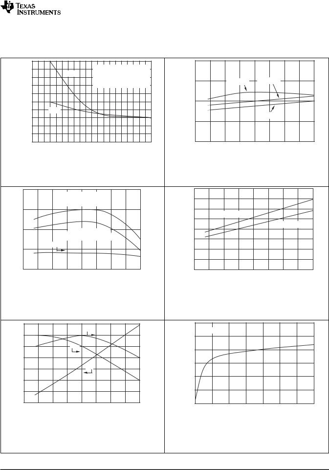
Figure 1. Open-Loop Gain and Phase vs Frequency |
Figure 2. Power Supply and Common-Mode Rejection Ratio |
|||||||||||||||||
|
|
|
|
|
|
|
|
|
|
|
|
|
|
|
|
vs Frequency |
|
|
|
|
100k |
|
|
|
|
|
|
|
|
10k |
|
|
140 |
|
|
|
|
|
|
|
|
|
|
|
|
|
|
|
|
|
|
|
130 |
|
|
|
|
|
|
(nVNoise√Hz) |
10k |
|
|
|
|
Current Noise |
|
1k |
|
Separation(dB) |
120 |
|
|
|
|
|
|
||
|
|
|
|
|
|
|
|
|
|
√ Hz) |
|
|
|
|
|
|
|||
|
|
|
|
|
|
|
|
|
|
|
|
|
|
|
|
|
|||
1k |
|
|
|
|
|
|
|
|
100 |
(fANoise |
110 |
|
|
|
|
|
|
||
|
|
|
|
|
|
|
|
|
|
|
|
|
|
|
|
|
|||
|
|
|
|
|
|
|
|
|
|
|
|
|
|
|
|
|
|
||
|
|
|
Voltage Noise |
|
|
|
|
|
|
|
|
100 |
|
|
|
|
|
|
|
|
100 |
|
|
|
|
|
|
10 |
|
|
|
|
|
|
|
|
|
||
Voltage |
|
|
|
|
|
|
|
|
Current |
Channel |
90 |
|
|
|
|
|
|
||
10 |
|
|
|
|
|
|
|
|
1 |
|
|
|
|
|
|
||||
|
|
|
|
|
|
|
|
|
|
|
|
|
|
|
|
|
|
|
|
|
|
|
|
|
|
|
|
|
|
|
|
|
80 |
|
|
|
|
|
|
|
|
|
|
|
|
|
|
|
|
|
|
|
70 |
Dual and quad devices. |
|
|
|
||
|
|
|
|
|
|
|
|
|
|
|
|
|
|
|
|
|
|||
|
1 |
|
|
|
|
|
|
|
|
0.1 |
|
|
60 |
|
|
|
|
|
|
|
10 |
|
100 |
1k |
|
10k |
100k |
1M |
|
10M |
|
|
|
|
|
|
|
|
|
|
|
|
|
|
|
10 |
100 |
1k |
10k |
100k |
1M |
10M |
|||||||
|
|
|
|
|
|
|
|
|
|
|
|
|
|||||||
|
|
|
|
|
Frequency (Hz) |
|
|
|
|
|
|
|
|
Frequency (Hz) |
|
|
|||
|
|
|
|
|
|
|
|
|
|
|
|
|
|
|
|
|
|
||
Figure 3. Input Voltage and Current Noise Spectral Density |
Figure 4. Channel Separation vs Frequency |
|
vs Frequency
1 |
|
|
|
|
|
1 |
G = 1 |
|
|
|
|
|
RL = 600Ω |
|
|
(−40dBc) |
|
|
|
|
|
|
|
|
VO = 2.5VPP |
|
|
||
|
|
|
|
|
|
|
|
|
|
0.1 |
G = 100, 3VPP (VO = 1V to 4V) |
|
|
(%) |
0.1 |
RL = 600Ω |
|
|
|
|
|
|
|
|
|||||
|
|
|
|
|
|
||||
THD+N(%) |
|
|
|
|
DistortionHarmonic |
(−60dBc) |
|
|
|
G = 10, 3VPP (VO = 1V to 4V) |
|
|
0.01 |
|
|
|
|||
0.01 |
|
|
|
|
|
|
|||
|
|
|
|
|
|
(−80dBc) |
|
|
|
|
G = 1, 3VPP (VO = 1V to 4V) |
|
|
|
|
|
|
|
|
0.001 |
Input goes through transition region |
|
|
|
0.001 |
|
|
|
|
|
|
|
|
|
|
|
|
||
|
G = 1, 2.5VPP (VO = 0.25V to 2.75V) |
|
|
|
(−100dBc) |
3rd−Harmonic |
|
|
|
|
|
|
|
|
|
|
|||
|
|
|
|
|
|
2nd−Harmonic |
|
||
|
Input does NOT go through transition region |
|
|
|
|
|
|
||
0.0001 |
|
|
|
|
|
0.0001 |
|
|
|
10 |
100 |
1k |
10k |
100k |
|
(−120dBc) 1k |
10k |
100k |
1M |
|
Frequency (Hz) |
Frequency (Hz) |
|
Figure 5. Total Harmonic Distortion + Noise vs Frequency |
Figure 6. Harmonic Distortion + Noise vs Frequency |
|
|
|
|
|
|
8 |
Submit Documentation Feedback |
Copyright © 2000–2015, Texas Instruments Incorporated |
|
Product Folder Links: OPA350 OPA2350 OPA4350 |
|
OPA350, OPA2350, OPA4350
www.ti.com |
SBOS099D –SEPTEMBER 2000–REVISED DECEMBER 2015 |
Typical Characteristics (continued)
All specifications at TA = 25°C, VS = 5 V, and RL = 1 kΩ connected to VS/2, unless otherwise noted. |
|
|
|
||||||||||||||||||||
|
0.5 |
|
|
|
|
|
|
|
|
|
|
|
|
130 |
|
|
|
|
|
|
|
|
|
|
|
|
|
|
|
G = 2 |
|
|
|
|
|
|
|
|
|
|
|
|
|
|
|
|
|
|
0.4 |
|
|
Phase |
VO = 1.4V |
|
|
|
|
|
|
|
|
|
|
|
|
|
|
|
|||
|
|
|
|
|
NTSC Signal Generator |
|
|
Open−LoopGain(dB) |
125 |
|
R |
|
= 10kΩ |
|
RL = 1kΩ |
|
|
|
|||||
|
|
|
|
|
|
|
|
|
|
|
|
|
|
||||||||||
|
|
|
|
|
|
See Figure 6 for test circuit. |
|
|
L |
|
|
|
|
||||||||||
|
|
|
|
|
|
|
|
|
|
|
|
|
|
|
|
||||||||
|
|
|
|
|
|
|
|
|
|
|
|
|
|
|
|
|
|||||||
|
0.3 |
|
|
|
|
|
|
|
|
|
|
|
|
|
|
|
|
|
|
|
|
|
|
|
|
|
|
|
|
|
|
|
|
|
|
|
120 |
|
|
|
|
|
|
|
|
|
|
|
0.2 |
|
Gain |
|
|
|
|
|
|
|
|
|
|
|
|
|
|
|
|
|
|
|
|
DifferentialGain(%) |
PhaseDifferential(°) |
|
|
|
|
|
|
|
|
|
|
|
|
|
|
|
|
|
RL = 600Ω |
|
|
||
|
|
|
|
|
|
|
|
|
|
|
115 |
|
|
|
|
|
|
|
|
|
|||
|
0.1 |
|
|
|
|
|
|
|
|
|
|
|
|
|
|
|
|
|
|
|
|
|
|
|
0 |
|
|
|
|
|
|
|
|
|
|
|
|
110 |
|
|
|
|
|
|
|
|
|
|
0 |
100 |
200 |
300 |
400 |
500 |
600 |
700 |
800 |
900 |
1000 |
|
−75 |
−50 |
−25 |
|
0 |
25 |
50 |
75 |
100 |
125 |
|
|
|
|
|
|
Resistive Load ( Ω ) |
|
|
|
|
|
|
|
|
|
Temperature ( °C) |
|
|
|
|||||
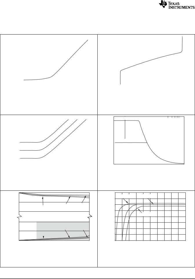
|
Figure 7. Differential Gain and Phase vs Resistive Load |
|
|
Figure 8. Open-Loop Gain vs Temperature |
|
||||||||||||||||||
100 |
|
|
|
|
|
|
|
|
|
110 |
|
|
40 |
|
|
|
|
|
|
|
|
|
|
|
|
|
|
CMRR, VS = 5.5V |
|
|
|
|
|
|
35 |
|
|
|
|
|
|
|
|
|
|||
|
|
|
|
(VCM = −0.1V to +5.6V) |
|
|
|
|
|
|
|
|
|
|
|
|
|
|
|||||
|
|
|
|
|
|
|
|
|
|
|
|
|
|
|
|
|
|
|
|||||
|
90 |
|
|
|
|
|
|
|
|
|
100 |
|
SlewRate (V/µs) |
30 |
Negative Slew Rate |
|
|
|
|
||||
|
|
|
|
|
|
|
|
|
|
|
|
|
|
|
|
|
|
||||||
CMRR(dB) |
|
|
|
|
|
|
|
|
|
|
|
PSRR(dB) |
25 |
|
|
|
|
|
|
|
|
|
|
|
|
|
|
|
|
|
|
|
|
|
|
|
|
|
|
|
Positive Slew Rate |
|
|||||
80 |
|
|
|
CMRR, VS = 2.7V |
|
|
|
90 |
20 |
|
|
|
|
|
|
|
|
|
|||||
|
|
|
(VCM =− 0.1V to +2.8V) |
|
|
|
15 |
|
|
|
|
|
|
|
|
|
|||||||
|
|
|
|
|
|
|
|
|
|
|
|
|
|
|
|
|
|
|
|
||||
|
|
PSRR |
|
|
|
|
|
|
|
|
|
|
|
|
|
|
|
|
|
||||
|
70 |
|
|
|
|
|
|
|
|
|
80 |
|
|
10 |
|
|
|
|
|
|
|
|
|
|
|
|
|
|
|
|
|
|
|
|
|
|
|
5 |
|
|
|
|
|
|
|
|
|
|
60 |
|
|
|
|
|
|
|
|
|
70 |
|
|
0 |
|
|
|
|
|
|
|
|
|
|
−75 |
−50 |
−25 |
0 |
25 |
50 |
|
75 |
100 |
125 |
|
|
−75 |
−50 |
−25 |
|
0 |
25 |
50 |
75 |
100 |
125 |
|
|
|
|
|
Temperature ( °C) |
|
|
|
|
|
|
|
|
|
|
Temperature ( °C) |
|
|
|
|||||
|
Figure 9. Common-Mode and Power-Supply Rejection Ratio |
|
|
Figure 10. Slew Rate vs Temperature |
|
||||||||||||||||||
|
|
|
|
vs Temperature |
|
|
|
|
|
|
|
|
|
|
|
|
|
|
|
||||
|
7.0 |
|
|
|
|
|
|
|
|
|
100 |
|
|
6.0 |
|
|
|
|
|
|
|
|
|
|
|
|
|
|
|
+ISC |
|
|
|
|
|
|
|
|
Per Amplifier |
|
|
|
|
|
|
|
|
|
6.5 |
|
|
|
|
|
|
|
|
|
90 |
Short−CircuitCurrent(mA) |
|
5.5 |
|
|
|
|
|
|
|
|
|
|
|
|
|
|
|
|
|
|
|
|
|
|
|
|
|
|
|
|
|
|
|
||
QuiescentCurrent(mA) |
6.0 |
|
|
−ISC |
|
|
|
|
|
80 |
QuiescentCurrent(mA) |
5.0 |
|
|
|
|
|
|
|
|
|
||
|
|
|
|
|
|
|
|
|
|
|
|
|
|
|
|
|
|
|
|
||||
5.5 |
|
|
|
|
|
|
|
|
|
70 |
|
|
|
|
|
|
|
|
|
|
|||
|
|
|
|
|
IQ |
|
|
|
|
|
4.5 |
|
|
|
|
|
|
|
|
|
|||
5.0 |
|
|
|
|
|
|
|
|
60 |
|
|
|
|
|
|
|
|
|
|
||||
4.5 |
|
|
|
|
|
|
|
|
|
50 |
4.0 |
|
|
|
|
|
|
|
|
|
|||
|
|
|
|
|
|
|
|
|
|
|
|
|
|
|
|
|
|
|
|||||
4.0 |
|
|
|
|
|
|
|
|
|
40 |
3.5 |
|
|
|
|
|
|
|
|
|
|||
|
|
|
|
|
|
|
|
|
|
|
|
|
|
|
|
|
|
|
|
|
|||
|
3.5 |
|
|
|
|
|
|
|
|
|
30 |
|
|
3.0 |
|
|
|
|
|
|
|
|
|
|
−75 |
−50 |
−25 |
0 |
25 |
50 |
|
75 |
100 |
125 |
|
|
|
2.0 |
2.5 |
3.0 |
3.5 |
|
4.0 |
4.5 |
5.0 |
5.5 |
|
|
|
|
|
|
|
|
|
|
|
|
|
|
|
|
|||||||||
|
|
|
|
Temperature ( °C) |
|
|
|
|
|
|
|
|
|
|
Supply Voltage (V) |
|
|
|
|||||
|
|
|
|
|
|
|
|
|
|
|
|
|
|
|
|
|
|
|
|
|
|||
|
Figure 11. Quiescent Current and short circuit Current vs |
|
Figure 12. Quiescent Current vs Supply Voltage |
||||||||||||||||||||
|
|
|
|
|
Temperature |
|
|
|
|
|
|
|
|
|
|
|
|
|
|
|
|
||
Copyright © 2000–2015, Texas Instruments Incorporated |
Submit Documentation Feedback |
9 |
Product Folder Links: OPA350 OPA2350 OPA4350
OPA350, OPA2350, OPA4350
SBOS099D –SEPTEMBER 2000 –REVISED DECEMBER 2015 |
www.ti.com |
Typical Characteristics (continued)
All specifications at TA = 25°C, VS = 5 V, and RL = 1 kΩ connected to VS/2, unless otherwise noted.
Current (pA) |
1k |
|
|
|
|
|
|
|
|
|
|
|
|
|
|
|
|
|
100 |
|
|
|
|
|
|
|
|
|
|
|
|
|
|
|
|
|
|
|
|
|
|
|
|
|
|
|
|
|
|
|
|
|
|
|
||
|
|
|
|
|
|
|
|
|
|
|
|
|
|
|
|
|
||
|
|
|
|
|
|
|
|
|
|
|
|
|
|
|
|
|
||
10 |
|
|
|
|
|
|
|
|
|
|
|
|
|
|
|
|
|
|
|
|
|
|
|
|
|
|
|
|
|
|
|
|
|
|
|
||
|
|
|
|
|
|
|
|
|
|
|
|
|
|
|
|
|
||
|
|
|
|
|
|
|
|
|
|
|
|
|
|
|
|
|
||
|
|
|
|
|
|
|
|
|
|
|
|
|
|
|
|
|
||
|
|
|
|
|
|
|
|
|
|
|
|
|
|
|
|
|
||
|
|
|
|
|
|
|
|
|
|
|
|
|
|
|
|
|
||
|
|
|
|
|
|
|
|
|
|
|
|
|
|
|
|
|
||
|
|
|
|
|
|
|
|
|
|
|
|
|
|
|
|
|
||
|
|
|
|
|
|
|
|
|
|
|
|
|
|
|
|
|
||
Bias |
|
|
|
|
|
|
|
|
|
|
|
|
|
|
|
|
|
|
|
|
|
|
|
|
|
|
|
|
|
|
|
|
|
|
|
|
|
|
|
|
|
|
|
|
|
|
|
|
|
|
|
|
|
|
|
|
|
|
|
|
|
|
|
|
|
|
|
|
|
|
|
|
|
|
|
|
|
|
|
|
|
|
|
|
|
|
|
|
|
|
|
|
|
|
Input |
1 |
|
|
|
|
|
|
|
|
|
|
|
|
|
|
|
|
|
|
|
|
|
|
|
|
|
|
|
|
|
|
|
|
|
|
||
|
|
|
|
|
|
|
|
|
|
|
|
|
|
|
|
|
||
|
|
|
|
|
|
|
|
|
|
|
|
|
|
|
|
|
||
0.1 |
|
|
|
|
|
|
|
|
|
|
|
|
|
|
|
|
|
|
|
|
|
|
|
|
|
|
|
|
|
|
|
|
|
|
|
||
|
|
|
|
|
|
|
|
|
|
|
|
|
|
|
|
|
|
|
|
|
|
|
|
|
|
|
|
|
|
|
|
|
|
|
|
|
|
|
|
|
|
|
|
|
|
|
|
|
|
|
|
|
|
|
|
|
|
|
|
|
|
|
|
|
|
|
|
|
|
|
|
|
|
|
|
|
|
|
|
|
|
|
|
|
|
|
|
|
|
|
|
|
|
|
|
|
|
|
|
|
|
|
|
|
|
|
|
|
|
|
|
|
|
|
−75 |
−50 |
−25 |
0 |
25 |
50 |
75 |
100 |
125 |
|||||||||
Temperature (°C)
Figure 13. Input Bias Current vs Temperature
|
100 |
|
|
|
|
|
|
|
|
|
|
|
|
|
|
|
|
|
|
|
|
|
|
|
|
|
|
|
|
|
|
|
|
|
|
|
|
|
|
(Ω) |
10 |
|
|
|
|
|
|
|
|
|
|
|
|
|
|
|
|
|
|
|
|
|
|
|
|
|
|
|
|
|
|
|
|
|
|
|
|
|
|
|
|
|
|
|
|
|
|
|
|
|
|
|
|
|
|
|
|
|
|
|
|
|
|
|
|
|
|
|
|
|
|
|
|
|
|
|
|
||
|
|
|
|
|
|
|
|
|
|
|
|
|
|
|
|
|
|
|
|
|
|
|
|
|
|
|
|
|
|
|
|
|
|
|
|
|
|
||
|
|
|
|
|
|
|
|
|
|
|
|
|
|
|
|
|
|
|
|
|
|
|
|
|
|
|
|
|
|
|
|
|
|
|
|
|
|
||
1 |
|
|
|
|
|
|
|
|
|
|
|
|
|
|
|
|
|
|
|
|
|
|
|
|
|
|
|
|
|
|
|
|
|
|
|
|
|
|
|
|
|
|
|
|
|
|
|
|
|
|
|
|
|
|
|
|
|
|
|
|
|
|
|
|
|
|
|
|
|
|
|
|
|
|
|
|
|
||
|
|
|
|
|
|
|
|
|
|
|
|
|
|
|
|
|
|
|
|
|
|
|
|
|
|
|
|
|
|
|
|
|
|
|
|
|
|
||
Impedance |
|
|
|
|
|
|
|
|
|
|
|
|
|
|
|
|
|
|
|
|
|
|
|
|
|
|
|
|
|
|
|
|
|
|
|
|
|
|
|
|
|
|
|
|
|
|
|
|
|
|
|
|
|
|
|
|
|
|
|
|
|
|
|
|
|
|
|
|
|
|
|
|
|
|
|
|
|
||
|
|
|
|
|
|
|
|
|
|
|
|
|
|
|
|
|
|
|
|
|
|
|
|
|
|
|
|
|
|
|
|
|
|
|
|
|
|
|
|
|
|
|
|
|
|
|
|
|
|
|
|
|
|
|
|
|
|
|
|
|
|
|
|
|
|
|
|
|
|
|
|
|
|
|
|
|
|
|
|
0.1 |
|
|
G = 100 |
|
|
|
|
|
|
|
|
|
|
|
|
|
|
|
|
|
|
|
|
|
|
|
|
|
|
|
|
|
|||||||
Output |
|
|
|
|
|
|
|
|
|
|
|
|
|
|
|
|
|
|
|
|
|
|
|
|
|
|
|
|
|
|
|
|
|
|
|
|
|
|
|
|
|
|
|
|
|
|
|
|
|
|
|
|
|
|
|
|
|
|
|
|
|
|
|
|
|
|
|
|
|
|
|
|
|
|
|
|
|
|
|
0.01 |
|
|
|
|
G |
= |
10 |
|
|
|
|
|
|
|
|
|
|
|
|
|
|
|
|
|
|
|
|
|
|
|
|
|
|
|
|
|
|
||
|
|
|
|
|
|
|
|
|
|
|
|
|
|
|
|
|
|
|
|
|
|
|
|
|
|
|
|
|
|
|
|
|
|
|
|||||
|
|
|
|
|
|
|
|
|
|
|
|
|
|
|
|
|
|
|
|
|
|
|
|
|
|
|
|
|
|
|
|
|
|
|
|||||
|
|
|
|
|
|
|
|
|
|
|
|
|
|
|
|
|
|
|
|
|
|
|
|
|
|
|
|
|
|
|
|
|
|
|
|
|
|
|
|
|
0.001 |
|
|
|
|
G = 1 |
|
|
|
|
|
|
|
|
|
|
|
|
|
|
|
|
|
|
|
|
|
|
|
|
|
|
|
|
|
|
|
||
|
|
|
|
|
|
|
|
|
|
|
|
|
|
|
|
|
|
|
|
|
|
|
|
|
|
|
|
|
|
|
|
|
|
|
|
||||
|
|
|
|
|
|
|
|
|
|
|
|
|
|
|
|
|
|
|
|
|
|
|
|
|
|
|
|
|
|
|
|
|
|
|
|
|
|
|
|
|
0.0001 |
|
|
|
|
|
|
|
|
|
|
|
|
|
|
|
|
|
|
|
|
|
|
|
|
|
|
|
|
|
|
|
|
|
|
|
|
|
|
|
|
|
|
|
|
|
|
|
|
|
|
|
|
|
|
|
|
|
|
|
|
|
|
|
|
|
|
|
|
|
|
|
|
|
|
|
|
|
|
|
|
|
|
|
|
|
|
|
|
|
|
|
|
|
|
|
|
|
|
|
|
|
|
|
|
|
|
|
|
|
|
|
|
|
|
|
|
|
|
|
|
|
|
|
|
|
|
|
|
|
|
|
|
|
|
|
|
|
|
|
|
|
|
|
|
|
|
|
|
|
|
|
|
|
|
100M |
|||
|
1 |
|
10 |
|
|
|
100 |
|
|
1k |
10k |
100k |
1M |
10M |
|||||||||||||||||||||||||
|
|
|
|
|
|
|
|
|
|
|
|
|
|
|
|
|
|
Frequency (Hz) |
|
|
|
|
|
|
|
|
|
|
|||||||||||
Figure 15. Closed-Loop Output Impedance vs Frequency
Output Voltage (V)
V+
(V+)−1
(V+)−2
(V−)+2
(V−)+1
(V−)
0
|
|
|
|
|
|
|
|
|
|
|
|
|
|
|
|
|
|
|
|
|
−55°C |
|
|
+25°C |
|
|
|||
|
|
+125°C |
|
|
|
|
||||||||
|
|
|
|
|
|
|
|
|
|
|
|
|
||
|
|
|
|
|
|
|
|
|
|
|
|
|
|
|
|
Depending on circuit configuration |
|
|
|||||||||||
|
|
|
|
|||||||||||
|
(including closed−loop gain) performance |
|
|
|||||||||||
|
may be degraded in shaded region. |
|
|
|||||||||||
|
|
|
|
|||||||||||
|
|
|
|
|
|
|
|
|
|
|
|
|
|
|
|
|
+125°C |
|
|
+25°C |
|
|
|
−55 °C |
|
|
|||
|
|
|
|
|
|
|
|
|
|
|
|
|
|
|
|
|
|
|
|
|
|
|
|
|
|
|
|
|
|
±10 |
±20 |
±30 |
±40 |
|||||||||||
|
|
Output Current (mA) |
|
|
|
|
|
|||||||
Figure 17. Output Voltage Swing vs Output Current
Current(pA) |
1.5 |
|
|
|
|
|
|
|
|
|
|
|
|
|
|
|
|
|
|
|
|
|
|
|
|
|
|
|
|
|
|
|
|
|
|
|
|
|
|
|
|
|
|
|
|
|
|
|
|
|
|
||
1.0 |
|
|
|
|
|
|
|
|
|
|
|
|
|
|
|
|
|
|
|
|
|
|
|
|
|
|
|
|
|
|
|
|
|
|
|
|
|
|
|
|
|
|
|
|
|
|
|
|
|
|
|
||
0.5 |
|
|
|
|
|
|
|
|
|
|
|
|
|
|
|
|
|
|
|
|
|
|
|
|
|
|
|
|
|
|
|
|
|
|
|
|
|
|
|
|
|
|
|
|
|
|
|
|
|
|
|
||
Bias |
|
|
|
|
|
|
|
|
|
|
|
|
|
|
|
|
|
|
|
|
|
|
|
|
|
|
Input |
0.0 |
|
|
|
|
|
|
|
|
|
|
|
|
|
|
|
|
|
|
|
|
|
|
|
|
|
|
|
|
|
|
|
|
|
|
|
|
|
|
|
|
|
|
|
|
|
|
|
|
|
|
|
|
|
−0.5 |
|
|
|
|
|
|
|
|
|
|
|
|
|
|
|
|
|
|
|
|
|
|
|
|
|
|
|
|
|
|
|
|
|
|
|
|
|
|
|
|
|
|
|
|
|
|
|
|
|
|
|
|
|
−0.5 |
0.0 |
0.5 |
1.0 |
1.5 |
2.0 |
2.5 |
3.0 |
3.5 |
4.0 |
4.5 |
5.0 |
5.5 |
|||||||||||||
|
|
|
|
|
|
|
|
Common−Mode Voltage (V) |
|
|
|
|
|
|
||||||||||||
Figure 14. Input Bias Current vs Input Common-Mode Voltage
|
6 |
|
|
|
|
|
|
|
|
|
|
|
|
|
|
|
|
|
|
|
|
|
|
|
|
|
|
|
|
|
|
|
|
|
|
|
VS |
= 5.5V |
|
|
|
|
|
|
|
|
|
|
|
|
|
|
|
Maximum output |
|
|
|
|
|
||||||||
|
5 |
|
|
|
|
|
|
|
|
|
|
|
|
|
|
|
|
|
|
|
voltage without |
|
|
|
|
|
|||||||
) |
|
|
|
|
|
|
|
|
|
|
|
|
|
|
|
|
|
|
|
slew rate−induced |
|
|
|
|
|
||||||||
|
|
|
|
|
|
|
|
|
|
|
|
|
|
|
|
|
|
|
|
|
|
|
|
|
|||||||||
|
|
|
|
|
|
|
|
|
|
|
|
|
|
|
|
|
|
|
|
|
|
|
|
|
|
|
|
|
|
|
|
|
|
PP |
|
|
|
|
|
|
|
|
|
|
|
|
|
|
|
|
|
|
|
|
distortion. |
|
|
|
|
|
|||||||
(V |
4 |
|
|
|
|
|
|
|
|
|
|
|
|
|
|
|
|
|
|
|
|
|
|
|
|
|
|
|
|
|
|
|
|
|
|
|
|
|
|
|
|
|
|
|
|
|
|
|
|
|
|
|
|
|
|
|
|
|
|
|
|
|
|
|
|
||
Voltage |
|
|
|
|
|
|
|
|
|
|
|
|
|
|
|
|
|
|
|
|
|
|
|
|
|
|
|
|
|
|
|
|
|
|
|
|
|
|
|
|
|
|
|
|
|
|
|
|
|
|
|
|
|
|
|
|
|
|
|
|
|
|
|
|
|
|
|
3 |
|
VS |
= 2.7V |
|
|
|
|
|
|
|
|
|
|
|
|
|
|
|
|
|
|
|
|
|
|
|
|
|
|
|
|||
Output |
|
|
|
|
|
|
|
|
|
|
|
|
|
|
|
|
|
|
|
|
|
|
|
|
|
|
|
|
|||||
2 |
|
|
|
|
|
|
|
|
|
|
|
|
|
|
|
|
|
|
|
|
|
|
|
|
|
|
|
|
|
|
|
|
|
|
|
|
|
|
|
|
|
|
|
|
|
|
|
|
|
|
|
|
|
|
|
|
|
|
|
|
|
|
|
|
|
||
|
|
|
|
|
|
|
|
|
|
|
|
|
|
|
|
|
|
|
|
|
|
|
|
|
|
|
|
|
|
|
|
|
|
|
1 |
|
|
|
|
|
|
|
|
|
|
|
|
|
|
|
|
|
|
|
|
|
|
|
|
|
|
|
|
|
|
|
|
|
|
|
|
|
|
|
|
|
|
|
|
|
|
|
|
|
|
|
|
|
|
|
|
|
|
|
|
|
|
|
|
|
|
|
|
|
|
|
|
|
|
|
|
|
|
|
|
|
|
|
|
|
|
|
|
|
|
|
|
|
|
|
|
|
|
|
|
|
0 |
|
|
|
|
|
|
|
|
|
|
|
|
|
|
|
|
|
|
|
|
|
|
|
|
|
|
|
|
|
|
|
|
|
|
|
|
|
|
|
|
|
|
|
|
|
|
|
|
|
|
|
|
|
|
|
|
|
|
|
|
|
|
|
|
|
|
|
|
|
|
|
|
|
|
|
|
|
|
|
|
|
|
|
|
|
|
|
|
|
|
|
|
|
|
|
|
|
|
|
|
|
100k |
|
|
|
|
|
|
|
|
1M |
|
|
|
|
|
|
|
10M |
|
100M |
|||||||||||||
|
|
|
|
|
|
|
|
|
|
|
|
|
|
Frequency (Hz) |
|
|
|
|
|
||||||||||||||
Figure 16. Maximum Output Voltage vs Frequency
|
140 |
|
|
|
|
|
|
|
|
|
|
|
130 |
IOUT = 250µA |
|
IOUT = 2.5mA |
|
|
|
|
|
||
|
|
|
|
|
|
|
|
|
|
|
|
(dB) |
120 |
|
|
|
|
|
|
|
|
|
|
|
|
|
|
|
|
|
|
|
|
|
|
Gain |
110 |
|
|
|
|
|
|
|
|
|
|
100 |
|
|
IOUT = 4.2mA |
|
|
|
|
|
|||
Open−Loop |
|
|
|
|
|
|
|
|
|
|
|
90 |
|
|
|
|
|
|
|
|
|
|
|
80 |
|
|
|
|
|
|
|
|
|
|
|
|
70 |
|
|
|
|
|
|
|
|
|
|
|
60 |
|
|
|
|
|
|
|
|
|
|
|
0 |
20 |
40 |
60 |
80 |
100 |
120 |
140 |
160 |
180 |
200 |
|
|
|
Output Voltage Swing from Rails (mV) |
|
|
||||||
Figure 18. Open-Loop Gain vs Output Voltage Swing
10 |
Submit Documentation Feedback |
Copyright © 2000–2015, Texas Instruments Incorporated |
Product Folder Links: OPA350 OPA2350 OPA4350
OPA350, OPA2350, OPA4350
www.ti.com |
SBOS099D –SEPTEMBER 2000–REVISED DECEMBER 2015 |
Typical Characteristics (continued) |
|
|
|
|
|
|
|
|
|
|
|
||||
All specifications at TA = 25°C, VS = 5 V, and RL = 1 kΩ connected to VS/2, unless otherwise noted. |
|
|
|||||||||||||
|
18 |
|
|
Typical distribution of |
|
|
20 |
|
|
|
|
|
|
|
Typical production |
|
16 |
|
|
|
|
18 |
|
|
|
|
|
|
|
||
|
|
|
packaged units. |
|
|
|
|
|
|
|
|
|
distribution of |
||
AmplifiersofPercent(%) |
14 |
|
|
|
|
AmplifiersofPercent(%) |
16 |
|
|
|
|
|
|
|
packaged units. |
12 |
|
|
|
|
14 |
|
|
|
|
|
|
|
|
||
|
10 |
|
|
|
|
|
12 |
|
|
|
|
|
|
|
|
|
8 |
|
|
|
|
|
10 |
|
|
|
|
|
|
|
|
|
|
|
|
|
|
|
|
|
|
|
|
|
|
|
|
|
6 |
|
|
|
|
|
8 |
|
|
|
|
|
|
|
|
|
|
|
|
|
|
|
|
|
|
|
|
|
|
|
|
|
4 |
|
|
|
|
|
6 |
|
|
|
|
|
|
|
|
|
|
|
|
|
|
|
|
|
|
|
|
|
|
|
|
|
2 |
|
|
|
|
|
4 |
|
|
|
|
|
|
|
|
|
|
|
|
|
|
|
|
|
|
|
|
|
|
|
|
|
0 |
|
|
|
|
|
2 |
|
|
|
|
|
|
|
|
|
|
|
|
|
|
|
|
|
|
|
|
|
|
|
|
|
− 500 −450 |
−400 −350 − 300 −250 −200 −150 −100 −50 |
0 50 |
100 150 200 250 300 350 400 450 |
500 |
|
0 |
|
|
|
|
|
|
|
|
|
|
0 |
1 |
2 3 |
4 5 |
6 |
7 |
8 |
9 |
10 11 12 13 14 15 |
|||||
Offset Voltage (µV) |
Offset Voltage Drift (µV/ °C) |
Figure 19. Offset Voltage Production Distribution |
Figure 20. Offset Voltage Drift Production Distribution |
|
80 |
|
|
|
|
|
|
10 |
|
|
|
70 |
|
|
|
|
|
|
|
|
|
|
|
|
G = 1 |
|
|
|
|
|
|
|
|
60 |
|
|
|
|
|
Settling Time(µs) |
|
0.01% |
|
Overshoot(%) |
|
|
|
|
|
|
|
|
||
50 |
|
|
|
|
|
|
|
|
||
|
G= −1 |
|
|
|
|
|
|
|||
40 |
|
|
|
|
|
1 |
|
|
||
30 |
|
|
|
|
|
|
|
|
||
|
|
|
G = ±10 |
|
|
|
|
|
||
|
20 |
|
|
|
|
|
|
|
|
|
|
10 |
|
|
|
|
|
|
|
0.1% |
|
|
|
|
|
|
|
|
|
|
|
|
|
0 |
|
|
|
|
|
|
0.1 |
|
|
|
10 |
100 |
1k |
10k |
100k |
1M |
|
−1 |
−10 |
−100 |
|
|
|
Load Capacitance (pF) |
|
|
|
|
Closed−Loop Gain (V/V) |
|
|
Figure 21. Small-Signal Overshoot vs Load Capacitance |
Figure 22. Settling Time vs Closed-Loop Gain |
50mV/div |
|
1V/div |
|
|
|
100ns/div |
200ns/div |
Figure 23. Small-Signal Step Response |
Figure 24. Large-Signal Step Response |
CL = 100 pF |
CL = 100 pF |
Copyright © 2000–2015, Texas Instruments Incorporated |
Submit Documentation Feedback |
11 |
Product Folder Links: OPA350 OPA2350 OPA4350
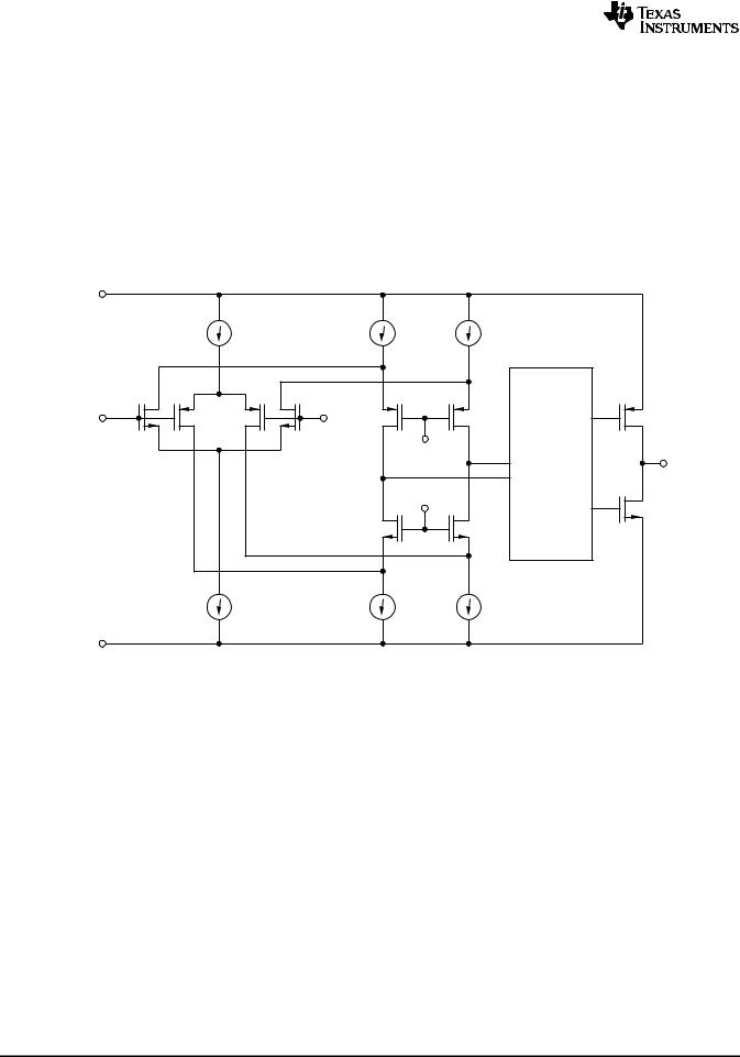
OPA350, OPA2350, OPA4350
SBOS099D –SEPTEMBER 2000 –REVISED DECEMBER 2015 |
www.ti.com |
7 Detailed Description
7.1 Overview
The OPA350 series rail-to-rail CMOS operational amplifiers are optimized for low voltage, single-supply operation. Rail-to-rail input and output, low noise (5 nV/√Hz), and high speed operation (38 MHz, 22 V/μs) make the amplifiers ideal for driving sampling Analog-to-Digital (A/D) converters. They are also suited for cell phone PA control loops and video processing (75-Ω drive capability), as well as audio and general purpose applications. Single, dual, and quad versions have identical specifications for maximum design flexibility.
7.2 Functional Block Diagram
V+ |
|
|
|
|
Reference |
|
|
|
Current |
|
|
VIN+ |
VIN− |
|
|
|
VBIAS1 |
Class AB |
|
|
|
Control |
VO |
|
|
Circuitry |
|
|
VBIAS2 |
|
|
V− |
|
|
|
(Ground) |
|
|
|
7.3 Feature Description
The OPA350 series of operational amplifiers (op amps) are fabricated on a state-of-the-art 0.6 micron CMOS process. They are unity-gain stable and suitable for a wide range of general purpose applications. Rail-to-rail input and output make them ideal for driving sampling A/D converters. They are also suited for controlling the output power in cell phones. These applications often require high speed and low noise. In addition, the OPA350 series offers a low-cost solution for general-purpose and consumer video applications (75-Ω drive capability).
Excellent AC performance makes the OPA350 series suited for audio applications. Their bandwidth, slew rate, low noise (5 nV/√Hz), low THD (0.0006%), and small package options are ideal for these applications. The class AB output stage is capable of driving 600-Ω loads connected to any point between V+ and ground.
Rail-to-rail input and output swing significantly increases dynamic range, especially in low voltage supply applications. Figure 25 shows the input and output waveforms for the OPA350 in unity-gain configuration. Operation is from a single 5-V supply with a 1-kΩ load connected to VS/2. The input is a 5 VPP sinusoid. Output voltage swing is approximately 4.95 VPP.
Power supply pins should be bypassed with 0.01-μF ceramic capacitors.
12 |
Submit Documentation Feedback |
Copyright © 2000–2015, Texas Instruments Incorporated |
Product Folder Links: OPA350 OPA2350 OPA4350

www.ti.com
Feature Description (continued)
5V
VIN
0
5V
VOUT
0
OPA350, OPA2350, OPA4350
SBOS099D –SEPTEMBER 2000–REVISED DECEMBER 2015
VS = +5, G = +1, RL = 1kΩ
1.25V/div
Figure 25. Rail-to-Rail Input and Output
7.3.1 Operating Voltage
OPA350 series operational amplifiers are fully specified from 2.7 V to 5.5 V. Supply voltage may range from 2.5 V to 5.5 V. Parameters are tested over the specified supply range: a feature of the OPA350 series. In addition, many specifications apply from −40°C to 85°C. Most behavior remains virtually unchanged throughout the full operating voltage range. Parameters that vary significantly with operating voltage or temperature are shown in
Typical Characteristics.
7.3.2 Rail-to-Rail Input
The tested input common-mode voltage range of the OPA350 series extends 100 mV beyond the supply rails. This is achieved with a complementary input stage: an N-channel input-differential pair in parallel with a P- channel differential pair, as shown in Figure 26. The N-channel pair is active for input voltages close to the positive rail, typically (V+) – 1.8 V to 100 mV above the positive supply, while the P-channel pair is on for inputs from 100 mV below the negative supply to approximately (V+) – 1.8 V. There is a small transition region, typically (V+) – 2 V to (V+) – 1.6 V, in which both pairs are on. This 400-mV transition region can vary ±400 mV with process variation. Thus, the transition region (both input stages on) can range from (V+) – 2.4 V to (V+) – 2 V on the low end, up to (V+) – 1.6 V to (V+) – 1.2 V on the high end.
Copyright © 2000–2015, Texas Instruments Incorporated |
Submit Documentation Feedback |
13 |
Product Folder Links: OPA350 OPA2350 OPA4350
Loading...