


MAX3221IPWR
MAX3221
3-V TO 5.5-V MULTICHANNEL RS-232 LINE DRIVER/RECEIVER
SLLS348B – JUNE 1999 – REVISED JANUARY 2000
D
Meets or Exceeds the Requirements of
TIA/EIA-232-F and ITU v.28 Standards
D
Operates With 3-V to 5.5-V VCC Supply
D
Operates up to 250 kbit/s
D
Low Standby Current ...1 µA Typical
D
External Capacitors ...4 × 0.1 µF
D
Accepts 5-V Logic Input With 3.3-V Supply
D
Designed to Be Interchangeable With
Maxim MAX3221
D
RS-232 Bus-Pin ESD Protection Exceeds
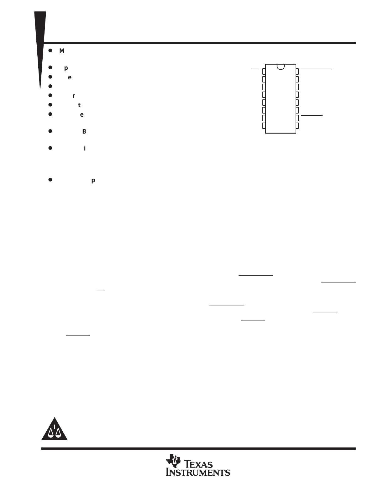
DB OR PW PACKAGE
(TOP VIEW)
EN
C1+
V+
C1–
C2+
C2–
V–
RIN
1
2
3
4
5
6
7
8
16
15
14
13
12
11
10
FORCEOFF
V
CC
GND
DOUT
FORCEON
DIN
INVALID
9
ROUT
±15-kV Using Human-Body Model (HBM)
D
Applications
– Battery-Powered Systems, PDAs,
Notebooks, Laptops, Palmtop PCs, and
Hand-Held Equipment
D
Package Options Include Plastic Shrink
Small-Outline (DB) and Thin Shrink
Small-Outline (PW) Packages
description
The MAX3221 device consists of one line driver , one line receiver , and a dual charge-pump circuit with ±15-kV
ESD protection pin to pin (serial-port connection pins, including GND). The device meets the requirements of
TIA/EIA-232-F and provides the electrical interface between an asynchronous communication controller and
the serial-port connector. The charge pump and four small external capacitors allow operation from a single 3-V
to 5.5-V supply . These devices operate at data signaling rates up to 250 kbit/s, and at a maximum of 30-V/µs
driver output slew rate.
Flexible control options for power management are available when the serial port is inactive. The
auto-powerdown feature functions when FORCEON is low and FORCEOFF
is high. During this mode of
operation, if the device does not sense a valid RS-232 signal, the driver outputs are disabled. If FORCEOFF
is set low and EN is high, both drivers and receivers are shut off, and the supply current is reduced to 1 µA.
Disconnecting the serial port or turning off the peripheral drivers causes the auto-powerdown condition to occur .
Auto-powerdown can be disabled when FORCEON and FORCEOFF are high. With auto-powerdown enabled,
the device is activated automatically when a valid signal is applied to any receiver input. The INVALID output
notifies the user if an RS-232 signal is present at any receiver input. INV ALID
is high (valid data) if any receiver
input voltage is greater than 2.7 V or less than –2.7 V, or has been between –0.3 V and 0.3 V for less than 30
µs. INV ALID is low (invalid data) if the receiver input voltage is between –0.3 V and 0.3 V for more than 30 µs.
Refer to Figure 5 for receiver input levels.
The MAX3221C is characterized for operation from 0°C to 70°C. The MAX3221I is characterized for operation
from –40°C to 85°C.
Please be aware that an important notice concerning availability, standard warranty, and use in critical applications of
Texas Instruments semiconductor products and disclaimers thereto appears at the end of this data sheet.
PRODUCT PREVIEW information concerns products in the formative or
design phase of development. Characteristic data and other
specifications are design goals. Texas Instruments reserves the right to
change or discontinue these products without notice.
Copyright 2000, Texas Instruments Incorporated
PRODUCT PREVIEW
POST OFFICE BOX 655303 • DALLAS, TEXAS 75265
1
MAX3221
OUTPUT
y
OUTPUT
3-V TO 5.5-V MULTICHANNEL RS-232 LINE DRIVER/RECEIVER
SLLS348B – JUNE 1999 – REVISED JANUARY 2000
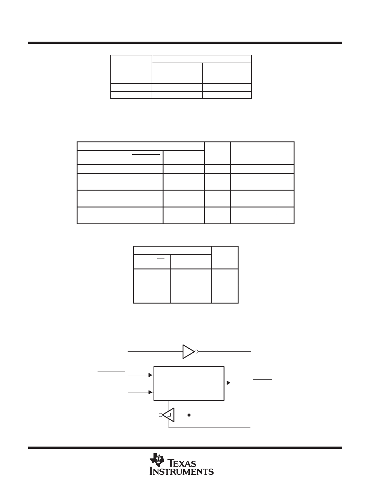
AVAILABLE OPTIONS
PACKAGED DEVICES
T
A
0°C to 70°C MAX3221CDB MAX3221CPW
–40°C to 85°C MAX3221IDB MAX3221IPW
The DB and PW packages are available taped and reeled. Add
the suffix R to device type (e.g., MAX3221CDBR).
SHRINK
SMALL OUTLINE
(DB)
Function Tables
EACH DRIVER
INPUTS
DIN FORCEON
X X L X Z Powered off
L H H X H
H HH XL
L L H Yes H
H LHYesL
L L H No Z
H L H No Z
H = high level, L = low level, X = irrelevant, Z = high impedance
FORCEOFF
VALID RIN
RS-232 LEVEL
THIN SHRINK
SMALL OUTLINE
(PW)
DOUT
auto-powerdown disabled
auto-powerdown enabled
auto-powerdown feature
DRIVER STATUS
Normal operation with
Normal operation with
Powered off by
PRODUCT PREVIEW
logic diagram (positive logic)
DIN
FORCEOFF
FORCEON
ROUT
EACH RECEIVER
INPUTS
RIN EN
L L X H
H LX L
X HX Z
Open L No H
H = high level, L = low level, X = irrelevant,
Z = high impedance (off), Open = disconnected
input or connected driver off
11
16
12
9
VALID RIN
RS-232 LEVEL
Auto-powerdown
ROUT
13
10
8
1
DOUT
INVALID
RIN
EN
2
POST OFFICE BOX 655303 • DALLAS, TEXAS 75265
MAX3221
Suppl
oltage
V
VIHDriver and control high-level input voltage
,,,
V
TAO erating free-air tem erature
°C
ICCSu ly current
3-V TO 5.5-V MULTICHANNEL RS-232 LINE DRIVER/RECEIVER
SLLS348B – JUNE 1999 – REVISED JANUARY 2000
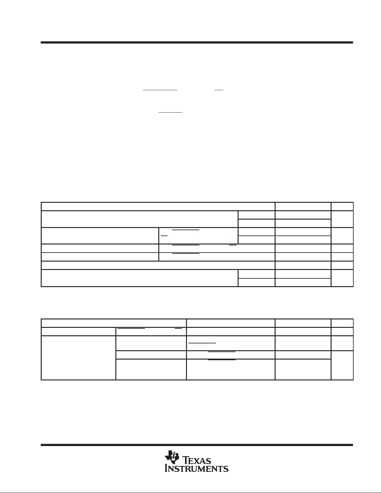
absolute maximum ratings over operating free-air temperature range (unless otherwise noted)
†
Supply voltage range, VCC (see Note 1) –0.3 V to 6 V. . . . . . . . . . . . . . . . . . . . . . . . . . . . . . . . . . . . . . . . . . . . . .
Positive output supply voltage range, V+ (see Note 1) –0.3 V to 7 V. . . . . . . . . . . . . . . . . . . . . . . . . . . . . . . . . .
Negative output supply voltage range, V– (see Note 1) 0.3 V to –7 V. . . . . . . . . . . . . . . . . . . . . . . . . . . . . . . . .
Supply voltage difference, V+
– V– (see Note 1) 13 V. . . . . . . . . . . . . . . . . . . . . . . . . . . . . . . . . . . . . . . . . . . . . . .
Input voltage range, VI: Driver (FORCEOFF, FORCEON, EN) –0.3 V to 6 V. . . . . . . . . . . . . . . . . . . . . . . . . . .
Receiver –25 V to 25 V. . . . . . . . . . . . . . . . . . . . . . . . . . . . . . . . . . . . . . . . . . . . . . . . . . . .
Output voltage range, VO: Driver –13.2 V to 13.2 V. . . . . . . . . . . . . . . . . . . . . . . . . . . . . . . . . . . . . . . . . . . . . . . . .
Receiver (INVALID) –0.3 V to VCC + 0.3 V. . . . . . . . . . . . . . . . . . . . . . . . . . . . . . . .
Package thermal impedance, θJA (see Note 2): DB package 82°C/W. . . . . . . . . . . . . . . . . . . . . . . . . . . . . . . . .
PW package 108°C/W. . . . . . . . . . . . . . . . . . . . . . . . . . . . . . . .
Lead temperature 1,6 mm (1/16 inch) from case for 10 seconds 260°C. . . . . . . . . . . . . . . . . . . . . . . . . . . . . . .
Storage temperature range, T
†
Stresses beyond those listed under “absolute maximum ratings” may cause permanent damage to the device. These are stress ratings only, and
functional operation of the device at these or any other conditions beyond those indicated under “recommended operating conditions” is not
implied. Exposure to absolute-maximum-rated conditions for extended periods may affect device reliability.
NOTES: 1. All voltages are with respect to network GND.
2. The package thermal impedance is calculated in accordance with JESD 51.
–65°C to 150°C. . . . . . . . . . . . . . . . . . . . . . . . . . . . . . . . . . . . . . . . . . . . . . . . . . .
stg
recommended operating conditions (see Note 3 and Figure 6)
MIN NOM MAX UNIT
pp
y v
p
V
V
V
NOTE 3: Test conditions are C1–C4 = 0.1 µF at VCC = 3.3 V ± 0.3 V; C1 = 0.047 µF, C2–C4 = 0.33 µF at VCC = 5 V ± 0.5 V.
Driver and control low-level input voltage DIN, FORCEOFF, FORCEON, EN 0.8 V
IL
Driver and control input voltage DIN, FORCEOFF, FORCEON 0 5.5 V
I
Receiver input voltage –25 25 V
I
p
p
DIN, FORCEOFF, FORCEON,
EN
VCC = 3.3 V 3 3.3 3.6
VCC = 5 V 4.5 5 5.5
VCC = 3.3 V 2
VCC = 5 V 2.4
MAX3221C 0 70
MAX3221I –40 85
°
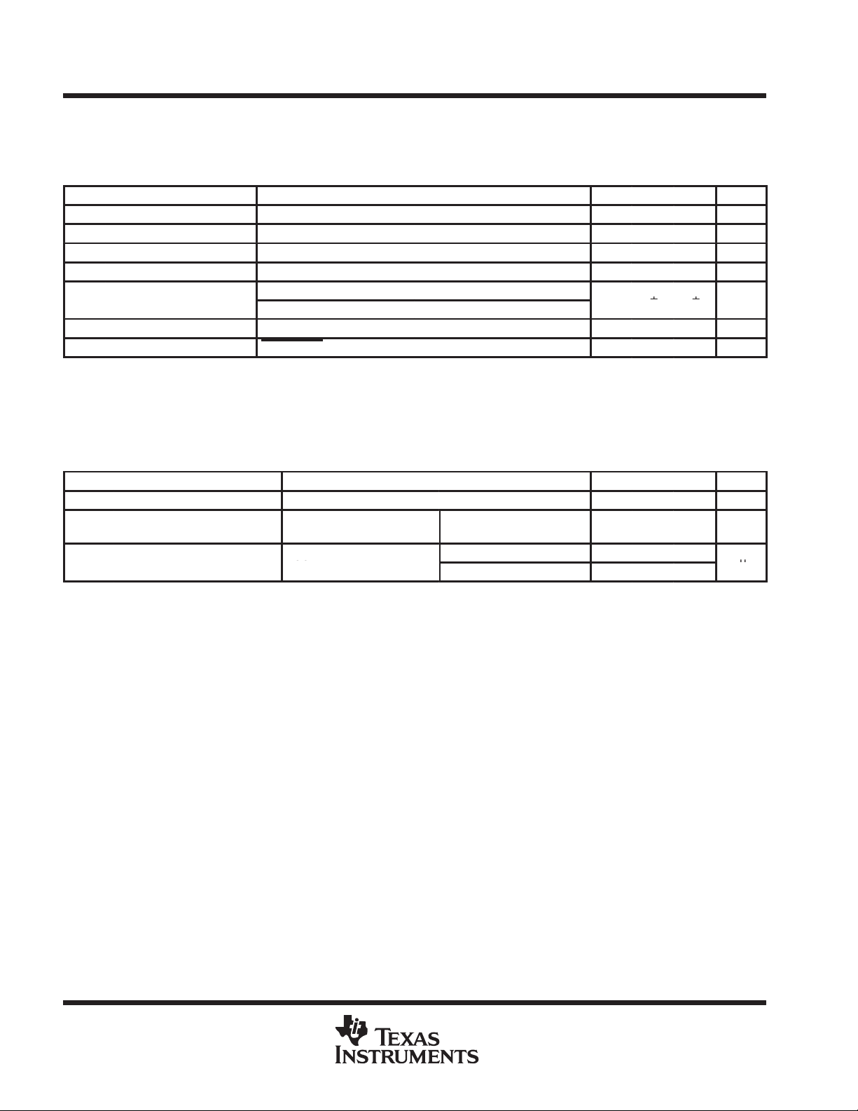
electrical characteristics over recommended ranges of supply voltage and operating free-air
temperature (unless otherwise noted) (see Note 3 and Figure 6)
PARAMETER TEST CONDITIONS MIN TYP‡MAX UNIT
I
Input leakage current FORCEOFF, FORCEON, EN ±0.01 ±1 µA
I
Auto-powerdown disabled
pp
‡
All typical values are at VCC = 3.3 V or VCC = 5 V, and TA = 25°C.
NOTE 3: Test conditions are C1–C4 = 0.1 µF at VCC = 3.3 V ± 0.3 V; C1 = 0.047 µF, C2–C4 = 0.33 µF at VCC = 5 V ± 0.5 V.
Powered off No load, FORCEOFF at GND 1 10
Auto-powerdown enabled
No load,
FORCEOFF
No load, FORCEOFF at VCC,
FORCEON at GND,
All RIN are open or grounded
and FORCEON at V
CC
0.3 1 mA
1 10
µA
PRODUCT PREVIEW
POST OFFICE BOX 655303 • DALLAS, TEXAS 75265
3
MAX3221
I
Sh
‡
±35
±60
mA
SR(tr)
g
CC
V/µs
3-V TO 5.5-V MULTICHANNEL RS-232 LINE DRIVER/RECEIVER
SLLS348B – JUNE 1999 – REVISED JANUARY 2000
DRIVER SECTION
electrical characteristics over recommended ranges of supply voltage and operating free-air
temperature (unless otherwise noted) (see Note 3 and Figure 6)
PARAMETER TEST CONDITIONS MIN TYP†MAX UNIT
V
High-level output voltage DOUT at RL = 3 kΩ to GND, DIN = GND 5 5.4 V
OH
V
Low-level output voltage DOUT at RL = 3 kΩ to GND, DIN = V
OL
I
High-level input current VI = V
IH
I
Low-level input current VI at GND ±0.01 ±1 µA
IL
OS
r
o
I
off
†
All typical values are at VCC = 3.3 V or VCC = 5 V, and TA = 25°C.
‡
Short-circuit durations should be controlled to prevent exceeding the device absolute power dissipation ratings, and not more than one output
should be shorted at a time.
NOTE 3: Test conditions are C1–C4 = 0.1 µF at VCC = 3.3 V ± 0.3 V; C1 = 0.047 µF, C2–C4 = 0.33 µF at VCC = 5 V ± 0.5 V.
ort-circuit output current
Output resistance VCC, V+, and V– = 0 V, VO = ±2 V 300 10M Ω
Output leakage current FORCEOFF = GND, VO = ±12 V, VCC = 0 to 5.5 V ±25 µA
CC
VCC = 3.6 V, VO = 0 V
VCC = 5.5 V, VO = 0 V
CC
–5 –5.4 V
±0.01 ±1 µA
switching characteristics over recommended ranges of supply voltage and operating free-air
temperature (unless otherwise noted) (see Note 3 and Figure 6)
PARAMETER TEST CONDITIONS MIN TYP†MAX UNIT
Maximum data rate CL = 1000 pF, RL = 3 kΩ, See Figure 1 250 kbit/s
t
sk(p)
†
All typical values are at VCC = 3.3 V or VCC = 5 V, and TA = 25°C.
§
Pulse skew is defined as |t
NOTE 3: Test conditions are C1–C4 = 0.1 µF at VCC = 3.3 V ± 0.3 V; C1 = 0.047 µF, C2–C4 = 0.33 µF at VCC = 5 V ± 0.5 V.
Pulse skew
Slew rate, transition region VCC = 3.3 V,
(see Figure 1)
§
– t
PLH
PHL
CL = 150 pF to 2500 pF
RL = 3 kΩ to 7 kΩ
| of each channel of the same device.
RL = 3 kΩ to 7 kΩ
See Figure 2
CL = 150 pF to 1000 pF 6 30
CL = 150 pF to 2500 pF 4 30
100 ns
PRODUCT PREVIEW
4
POST OFFICE BOX 655303 • DALLAS, TEXAS 75265
 Loading...