


Texas Instruments DV2002TL2, BQ2002TSNTR, BQ2002TSN, BQ2002TPN, BQ2002DSNTR Datasheet
...bq2002D/T
NiCd/NiMH Fast-Charge Management ICs
Features
Fast charge of nickel cadmium or nickel-metal hydride batteries
Direct LED output displays charge status
Fast-charge termination by rate of rise of temperature, maximum voltage, maximum temperature, and maximum time
Internal band-gap voltage reference
Optional top-off charge (bq2002T only)
Selectable pulse-trickle charge rates (bq2002T only)
Low-power mode
8-pin 300-mil DIP or 150-mil SOIC
General Description
The bq2002D/T Fast-Charge IC are low-cost CMOS battery-charge controllers able to provide reliable charge termination for both NiCd and NiMH battery applications. Controlling a current-limited or constant-current supply allows the bq2002D/T to be the basis for a cost-effective stand-alone or system-integrated charger. The bq2002D/T integrates fast charge with optional top-off and pulsed-trickle control in a single IC for charging one or more NiCd or NiMH battery cells.
Fast charge is initiated on application of the charging supply or battery replacement. For safety, fast charge is inhibited if the battery temperature and voltage are outside configured limits.
Fast charge is terminated by any of the following:
Rate of temperature rise
Maximum voltage
Maximum temperature
Maximum time
After fast charge, the bq2002T optionally tops-off and pulse-trickles the battery per the pre-configured limits. Fast charge may be inhibited using the INH pin. The bq2002D/T may be placed in low-standby-power mode to reduce system power consumption.
Pin Connections |
|
|
|
Pin Names |
|
|
|
|
||||||||||
|
|
|
|
|
|
|
|
|
|
TM |
Timer mode select input |
TS |
Temperature sense input |
|||||
|
TM |
1 |
8 |
|
CC |
|
||||||||||||
|
|
|
|
|
|
|
|
|
|
|
|
|||||||
|
|
|
|
|
|
|
|
|
|
|
|
|
|
|
VCC |
Supply voltage input |
||
|
|
|
2 |
7 |
|
|
|
|
LED |
Charging status output |
||||||||
|
LED |
|
INH |
|
||||||||||||||
|
|
|
|
|
|
|
|
|
|
|
|
|||||||
|
BAT |
3 |
6 |
|
VCC |
|
BAT |
Battery voltage input |
INH |
Charge inhibit input |
||||||||
|
|
|
|
|
|
|
|
|
|
|
|
|||||||
VSS |
4 |
5 |
|
TS |
|
VSS |
System ground |
CC |
Charge control output |
|||||||||
|
|
|
|
8-Pin DIP or |
|
|
|
|
|
|
|
|
|
|
|
|
||
|
|
|
|
Narrow SOIC |
|
|
|
|
|
|
|
|
|
|
|
|
||
|
|
|
|
|
PN-200201.eps |
|
|
|
|
|
|
|
|
|
|
|||
|
|
|
|
|
|
|
|
|
|
|
||||||||
|
|
|
|
|
|
|
|
|
|
|||||||||
bq2002D/T Selection Guide |
|
|
|
|
|
|
||||||||||||
|
|
|
|
|
|
|
|
|
|
|
|
|
|
|
||||
Part No. |
|
|
TCO |
|
HTF |
|
|
|
LTF |
|
Fast Charge |
Time-Out |
Top-Off |
Maintenance |
||||
|
|
|
|
|
0.225 VCC |
|
0.25 VCC |
|
0.4 VCC |
|
C/4 |
320 min |
C/64 |
C/256 |
||||
bq2002D |
|
|
|
|
|
1C |
80 min |
C/16 |
C/256 |
|||||||||
|
|
|
|
|
|
|
|
|
|
|
|
|
|
|
2C |
40 min |
None |
C/128 |
|
|
|
|
|
0.225 VCC |
|
0.25 VCC |
|
|
|
|
|
C/4 |
440 min |
None |
None |
||
bq2002T |
|
|
|
|
|
|
None |
|
1C |
110 min |
None |
None |
||||||
|
|
|
|
|
|
|
|
|
|
|
|
|
|
|
2C |
55 min |
None |
None |
SLUS133–JANUARY 2000 E
1
bq2002D/T
Pin Descriptions
TM |
Timer mode input |
|
A three-level input that controls the settings |
|
for the fast charge safety timer, voltage ter- |
|
mination mode, top-off, pulse-trickle, and |
|
voltage hold-off time. |
LED |
Charging output status |
|
Open-drain output that indicates the charging |
|
status. |
BAT |
Battery input voltage |
|
The battery voltage sense input. The input to |
|
this pin is created by a high-impedance re- |
|
sistor divider network connected between |
|
the positive and negative terminals of the |
|
battery. |
VSS |
System ground |
TS |
Temperature sense input |
|
Input for an external battery temperature |
|
monitoring thermistor. |
VCC |
Supply voltage input |
|
5.0V ±20% power input. |
INH |
Charge inhibit input |
|
When high, INH suspends the fast charge in |
|
progress. When returned low, the IC re- |
sumes operation at the point where initially suspended.
CCCharge control output
An open-drain output used to control the charging current to the battery. CC switching to high impedance (Z) enables charging current to flow, and low to inhibit charging current. CC is modulated to provide top-off, if enabled, and pulse trickle.
Functional Description
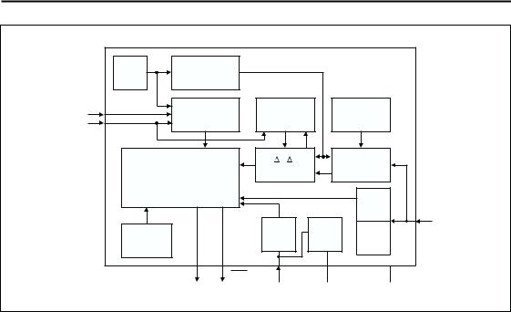
Figures 2 and 3 show state diagrams of bq2002D/T and Figure 4 shows the block diagram of the bq2002D/T
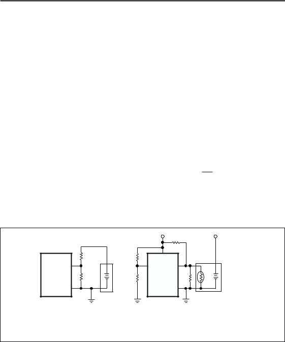
Battery Voltage and Temperature
Measurements
Battery voltage and temperature are monitored for maximum allowable values. The voltage presented on the battery sense input, BAT, should represent a single-cell potential for the battery under charge. A resistor-divider ratio of:
RB1 = N - 1
RB2
is recommended to maintain the battery voltage within the valid range, where N is the number of cells, RB1 is the resistor connected to the positive battery terminal, and RB2 is the resistor connected to the negative battery terminal. See Figure 1.
|
|
|
VCC |
|
PACK + |
|
|
|
|
RT1 |
|
|
RB1 |
R3 |
VCC |
|
|
BAT |
|
|
TM |
TS |
|
bq2002D/T |
|
|
bq2002D/T RT2 |
N |
|
RB2 |
R4 |
T |
|||
|
|
|
|
|
C |
VSS |
|
|
|
VSS |
|
BAT pin connection |
Mid-level |
Thermistor connection |
|||
|
|
setting for TM |
|
|
|
NTC = negative temperature coefficient thermistor.
F2002DT1.eps
Figure 1. Voltage and Temperature Monitoring and TM Pin Configuration
2

|
|
|
|
|
|
|
|
|
|
|
bq2002D/T |
|
Chip on |
|
Battery Voltage |
|
|
|
|
|
|
||
V |
CC |
4.0V |
|
|
too High? |
V |
|
|
|
|
|
|
|
|
|
|
|
|
|
|
|
||
|
|
|
|
|
|
BAT > 2V |
|
|
|
|
|
|
|
V |
BAT |
< 2V |
|
|
|
|
|
|
|
|
|
|
|
|
|
|
|
|
|
||
VTS > 0.25V VCC |
|
|
Battery |
|
|
|
|
|
|
||
|
|
|
|
|
Temperature? |
VTS < 0.25V |
VCC |
|
|
||
|
|
|
|
|
|
Charge |
|
||||
|
|
|
|
|
|
|
|
|
|
|
|
|
|
|
|
|
|
|
|
|
|
Pending |
|
|
|
Fast Charge, |
|
|
|
|
|
|
|
Off, |
|
|
|
|
|
|
|
|
|
CC = Low |
|
||
|
|
CC = Z |
|
|
|
|
|
|
|
||
|
|
|
|
|
|
|
|
LED = Low |
|
||
|
|
LED = Low |
|
|
V |
BAT |
< 2V and |
|
|
||
|
|
|
|
|
|
|
|
||||
|
|
|
|
|
|
|
|
|
|||
|
|
|
|
|
VTS > 0.25V VCC |
|
VBAT > 2V |
|
|||
|
|
|
|
|
|
|
|
|
|
|
|
|
|
T/ |
t or |
|
|
|
|
|
|
|
|
|
|
VBAT > 2V or |
|
|
|
|
VBAT |
2V |
|||
|
|
VTS < 0.25V VCC or |
|
|
|
|
|||||
|
|
Maximum Time Out |
|
|
|
|
Off, |
|
|||
|
|
|
|
|
CC = Low |
|
|||||
|
|
|
|
|
|
|
|
|
|
||
|
|
|
|
|
|
|
|
|
LED = Z |
|
|
SD2002D.eps
Figure 2. bq2002D State Diagram
|
Chip on |
|
|
Battery Voltage |
|
|
|
|
|
|||
V |
CC |
4.0V |
|
|
too High? |
V |
|
|
|
|
||
|
|
|
|
|
|
|
|
|
|
|
||
|
|
|
|
|
|
|
|
BAT > 2V |
|
|
|
|
|
|
|
V |
BAT |
< 2V |
|
|
|
|
|
|
|
|
|
|
|
|
|
|
|
|
|
|
||
0.25 VCC < VTS < 0.6 |
VCC |
|
|
Battery |
|
|
|
|
|
|||
|
|
|
|
|
|
|
|
|
|
|
||
|
|
|
|
|
|
Temperature? |
VTS > 0.6 |
VCC or |
|
|
||
|
|
|
|
|
|
|
|
|
|
|||
|
|
|
|
|
|
|
|
VTS < 0.25 |
VCC |
Charge |
|
|
( T/ t or |
|
|
|
|
|
|
|
|
|
|
Pending |
|
|
|
|
|
|
|
|
|
|
|
|
|
|
Maximum Time Out) |
|
Fast |
|
|
|
|
|
|
Trickle |
|
||
and TM = High |
|
LED = |
|
|
|
|
|
|
LED = |
|
||
|
|
|
Low |
|
|
|
|
|
|
Low |
|
|
|
|
|
|
|
|
|
|
VBAT < 2V and |
|
|
||
|
|
|
VBAT > 2V or |
|
VTS < 0.6 |
VCC and |
VBAT > 2V |
|
||||
Top-off |
|
VCC or |
VTS > 0.25 |
VCC |
|
|
||||||
LED = Z |
|
VTS < 0.225 |
|
|
|
|
|
|||||
|
(( T/ |
t or |
|
|
|
|
|
|
||||
|
|
|
|
|
|
|
|
|
||||
|
|
|
Maximum Time Out) |
|
|
|
VBAT |
2V |
||||
|
|
|
and TM = High) |
|
|
|
||||||
|
|
|
|
|
Trickle |
|
||||||
VBAT > 2V or |
|
|
|
|
|
|
|
|
|
|
||
|
|
|
|
|
|
|
|
|
LED = Z |
|
||
VTS < 0.225 VCC or |
|
|
|
|
|
|
|
|
|
|
|
|
Maximum Time Out |
|
|
|
|
|
|
|
|
|
|
SD2002T.eps |
|
Figure 3. bq2002T State Diagram
3
bq2002D/T
|
Clock |
|
|
|
|
|
OSC |
Phase |
|
|
|
|
|
|
Generator |
|
|
|
|
|
TM |
Timing |
|
Sample |
Voltage |
|
|
|
|
|
||||
|
Control |
|
History |
Reference |
|
|
INH |
|
|
|
|
|
|
|
|
|
T/ t |
A to D |
|
|
|
Charge-Control |
|
ALU |
Converter |
|
|
|
State Machine |
|
|
|
|
|
|
|
|
|
|
HTF/ |
|
|
|
|
|
|
LTF |
|
|
|
|
|
|
Check |
|
Power-On |
|
MCV |
Power |
TCO |
TS |
|
|
Check |
Down |
|
|||
Reset |
|
Check |
|
|||
|
|
|
|
|||
|
CC |
LED |
BAT |
VCC |
VSS |
|
|
|
|
|
|
|
Bd2002TD.eps |
Figure 4. Block Diagram
Note: This resistor-divider network input impedance to end-to-end should be at least 200kΩ and less than 1 MΩ.
A ground-referenced negative temperature coefficient thermistor placed in proximity to the battery may be used as a low-cost temperature-to-voltage transducer. The temperature sense voltage input at TS is developed using a resistor-thermistor network between VCC and VSS. See Figure 1.
Starting A Charge Cycle
Either of two events starts a charge cycle (see Figure 5):
1.Application of power to VCC or
2.Voltage at the BAT pin falling through the maximum cell voltage where:
VMCV = 2V ±5%.
If the battery is within the configured temperature and voltage limits, the IC begins fast charge. The valid battery voltage range is VBAT < VMCV. The valid temperature range is VHTF < VTS < VLTF for the bq2002T and VHTF < VTS for the bq2002D where:
VLTF = 0.4 VCC ±5%.
VHTF = 0.25 VCC ±5% (bq2002T only).
If the battery voltage or temperature is outside of these limits, the IC pulse-trickle charges until the temperature falls within the allowed fast charge range or a new charge cycle is started.
Fast charge continues until termination by one or more of the four possible termination conditions:
Rate of temperature rise
Maximum voltage
Maximum temperature
Maximum time
∆T/∆t Termination
The bq2002D/T samples at the voltage at the TS pin every 19s and compares it to the value measured three samples earlier. If the voltage has fallen 25.6mV or more, fast charge is terminated. The ∆T/∆t termination test is valid only when VTCO < VTS < VLTF for the bq2002T and VTCO < VTS for the bq2002D.
Temperature Sampling
A sample is taken by averaging together 16 measurements taken 57µs apart. The resulting sample period (18.18ms) filters out harmonics around 55Hz. This tech-
4
 Loading...