


|
|
|
|
|
|
A741, A741Y |
|
|
|
GENERAL-PURPOSE OPERATIONAL AMPLIFIERS |
|||||
|
|
SLOS094B ± NOVEMBER 1970 ± REVISED SEPTEMBER 2000 |
|||||
|
|
|
|
|
|
|
|
D |
Short-Circuit Protection |
A741M . . . J PACKAGE |
|||||
D Offset-Voltage Null Capability |
|
(TOP VIEW) |
|
|
|||
|
|
|
|
|
|
||
D Large Common-Mode and Differential |
NC |
|
|
|
NC |
||
1 |
14 |
|
|||||
|
Voltage Ranges |
|
|||||
|
NC |
2 |
13 |
|
NC |
||
D No Frequency Compensation Required |
|
||||||
OFFSET N1 |
3 |
12 |
|
NC |
|||
|
Low Power Consumption |
|
|||||
D |
IN± |
4 |
11 |
|
VCC + |
||
D |
No Latch-Up |
IN+ |
5 |
10 |
|
OUT |
|
D Designed to Be Interchangeable With |
VCC ± |
6 |
9 |
|
OFFSET N2 |
||
|
Fairchild A741 |
NC |
7 |
8 |
|
NC |
|
description |
|
|
|
||||
A741M . . . JG PACKAGE |
|||||||
|
|
A741C, A741I . . . D, P, OR PW PACKAGE |
|||||
The A741 is a general-purpose operational amplifier featuring offset-voltage null capability.
The high common-mode input voltage range and the absence of latch-up make the amplifier ideal for voltage-follower applications. The device is short-circuit protected and the internal frequency compensation ensures stability without external components. A low value potentiometer may be connected between the offset null inputs to null out the offset voltage as shown in Figure 2.
(TOP VIEW)
OFFSET N1 |
1 |
8 |
NC |
IN± |
2 |
7 |
VCC+ |
IN+ |
3 |
6 |
OUT |
VCC ± |
4 |
5 |
OFFSET N2 |
A741M . . . U PACKAGE
(TOP VIEW)
The A741C is characterized for operation from |
NC |
|
|
1 |
10 |
|
NC |
|
|
|
|
|
|||
0°C to 70°C. The A741I is characterized for |
OFFSET N1 |
|
|
2 |
9 |
|
NC |
operation from ±40°C to 85°C.The A741M is |
IN± |
|
|
3 |
8 |
|
VCC + |
characterized for operation over the full military |
IN+ |
|
|
4 |
7 |
|
OUT |
temperature range of ±55°C to 125°C. |
VCC ± |
|
|
5 |
6 |
|
OFFSET N2 |
|
|
|
|
|
|
|
|
symbol |
|
A741M . . . FK PACKAGE |
||||
|
|
|||||
OFFSET N1 |
|
|
(TOP VIEW) |
|
||
IN + |
+ |
NC |
N1 |
|
|
|
|
OUT |
OFFSET NC NC NC |
|
|||
|
|
|
|
|
|
|
IN ± |
± |
|
|
|
|
|
OFFSET N2 |
|
|
|
|
|
|
|
NC |
3 |
2 |
1 |
20 19 |
NC |
|
4 |
|
|
18 |
||
|
IN± |
5 |
|
|
17 |
VCC + |
|
NC |
6 |
|
|
16 |
NC |
|
IN+ |
7 |
|
|
15 |
OUT |
|
NC |
8 |
|
|
14 |
NC |
|
|
9 |
10 11 12 13 |
|
||
|
|
NC |
CC± |
NC |
N2 NC |
|
|
|
|
V |
|
OFFSET |
|
|
NC ± No internal connection |
|
||||
PRODUCTION DATA information is current as of publication date. Products conform to specifications per the terms of Texas Instruments standard warranty. Production processing does not necessarily include testing of all parameters.
Copyright 2000, Texas Instruments Incorporated
POST OFFICE BOX 655303 •DALLAS, TEXAS 75265 |
1 |
A741, A741Y
GENERAL-PURPOSE OPERATIONAL AMPLIFIERS
SLOS094B ± NOVEMBER 1970 ± REVISED SEPTEMBER 2000
AVAILABLE OPTIONS
|
|
|
PACKAGED DEVICES |
|
|
CHIP |
|||
|
|
|
|
|
|
|
|
||
|
SMALL |
CHIP |
CERAMIC |
CERAMIC |
PLASTIC |
|
FLAT |
||
TA |
TSSOP |
FORM |
|||||||
OUTLINE |
CARRIER |
DIP |
DIP |
DIP |
PACK |
||||
|
(PW) |
(Y) |
|||||||
|
(D) |
(FK) |
(J) |
(JG) |
(P) |
(U) |
|||
|
|
|
|||||||
|
|
|
|
|
|
|
|
|
|
0°C to 70°C |
A741CD |
|
|
|
A741CP |
A741CPW |
|
A741Y |
|
|
|
|
|
|
|
|
|
|
|
± 40°C to 85°C |
A741ID |
|
|
|
A741IP |
|
|
|
|
|
|
|
|
|
|
|
|
|
|
± 55°C to 125°C |
|
A741MFK |
A741MJ |
A741MJG |
|
|
A741MU |
|
|
|
|
|
|
|
|
|
|
|
|
The D package is available taped and reeled. Add the suffix R (e.g., A741CDR).
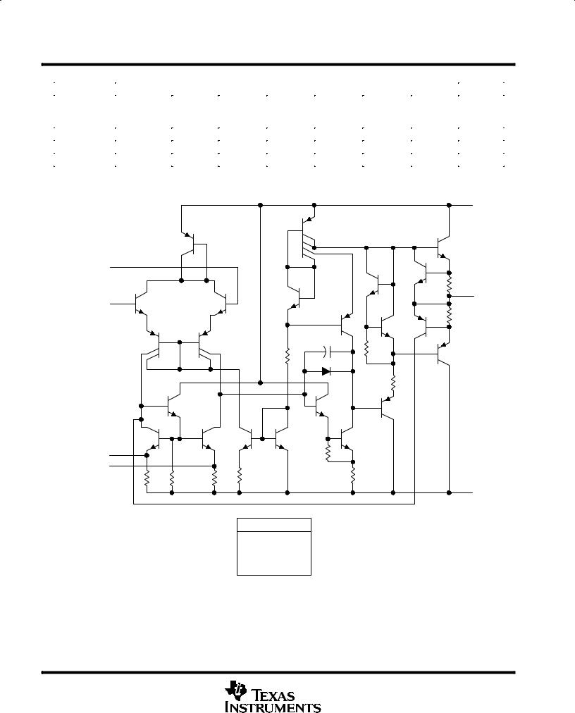
schematic
VCC+
IN ±
OUT
IN+
OFFSET N1
OFFSET N2
VCC ±
Component Count
Transistors 22
Resistors 11
Diode 1
Capacitor 1
2 |
POST OFFICE BOX 655303 •DALLAS, TEXAS 75265 |

A741, A741Y
GENERAL-PURPOSE OPERATIONAL AMPLIFIERS
SLOS094B ± NOVEMBER 1970 ± REVISED SEPTEMBER 2000
A741Y chip information
This chip, when properly assembled, displays characteristics similar to the A741C. Thermal compression or ultrasonic bonding may be used on the doped-aluminum bonding pads. Chips may be mounted with conductive epoxy or a gold-silicon preform.
BONDING PAD ASSIGNMENTS
(7) (6)
(8)
45
(5)
(1)
(4)
(2) |
(3) |
36
|
|
|
|
|
VCC+ |
||||
IN + |
(3) |
+ |
|
|
(7) |
|
|||
|
|
||||||||
|
|
|
|
|
|||||
|
|
|
|
(6) |
|||||
|
|
|
|
||||||
|
|
|
|
|
|
|
|||
IN ± |
(2) |
± |
|
|
|
|
OUT |
||
|
|
|
|
||||||
|
|
|
|
|
|||||
OFFSET N1 |
|
(1) |
|
|
|
|
(4) |
|
|
OFFSET N2 |
|
(5) |
|
|
VCC ± |
||||
CHIP THICKNESS: 15 TYPICAL BONDING PADS: 4 × 4 MINIMUM TJmax = 150°C.
TOLERANCES ARE ± 10%.
ALL DIMENSIONS ARE IN MILS.
POST OFFICE BOX 655303 •DALLAS, TEXAS 75265 |
3 |
A741, A741Y
GENERAL-PURPOSE OPERATIONAL AMPLIFIERS
SLOS094B ± NOVEMBER 1970 ± REVISED SEPTEMBER 2000
absolute maximum ratings over operating free-air temperature range (unless otherwise noted)²
|
|
A741C |
A741I |
A741M |
UNIT |
|
|
|
|
|
|
Supply voltage, VCC+ (see Note 1) |
|
18 |
22 |
22 |
V |
Supply voltage, VCC ± (see Note 1) |
|
±18 |
± 22 |
± 22 |
V |
Differential input voltage, VID (see Note 2) |
|
±15 |
±30 |
±30 |
V |
Input voltage, VI any input (see Notes 1 and 3) |
|
±15 |
±15 |
±15 |
V |
Voltage between offset null (either OFFSET N1 or OFFSET N2) and VCC ± |
±15 |
±0.5 |
±0.5 |
V |
|
Duration of output short circuit (see Note 4) |
|
unlimited |
unlimited |
unlimited |
|
|
|
|
|
|
|
Continuous total power dissipation |
|
See Dissipation Rating Table |
|
||
|
|
|
|
|
|
Operating free-air temperature range, TA |
|
0 to 70 |
± 40 to 85 |
± 55 to 125 |
°C |
Storage temperature range |
|
± 65 to 150 |
± 65 to 150 |
± 65 to 150 |
°C |
|
|
|
|
|
|
Case temperature for 60 seconds |
FK package |
|
|
260 |
°C |
|
|
|
|
|
|
Lead temperature 1,6 mm (1/16 inch) from case for 60 seconds |
J, JG, or U package |
|
|
300 |
°C |
|
|
|
|
|
|
Lead temperature 1,6 mm (1/16 inch) from case for 10 seconds |
D, P, or PW package |
260 |
260 |
|
°C |
|
|
|
|
|
|
²Stresses beyond those listed under ªabsolute maximum ratingsº may cause permanent damage to the device. These are stress ratings only, and functional operation of the device at these or any other conditions beyond those indicated under ªrecommended operating conditionsº is not implied. Exposure to absolute-maximum-rated conditions for extended periods may affect device reliability.
NOTES: 1. All voltage values, unless otherwise noted, are with respect to the midpoint between VCC+ and VCC ±.
2.Differential voltages are at IN+ with respect to IN ±.
3.The magnitude of the input voltage must never exceed the magnitude of the supply voltage or 15 V, whichever is less.
4.The output may be shorted to ground or either power supply. For the A741M only, the unlimited duration of the short circuit applies at (or below) 125°C case temperature or 75°C free-air temperature.
DISSIPATION RATING TABLE
PACKAGE |
TA ≤ 25°C |
DERATING |
DERATE |
TA = 70°C |
TA = 85°C |
TA = 125°C |
|
POWER RATING |
FACTOR |
ABOVE TA |
POWER RATING |
POWER RATING |
POWER RATING |
||
|
|||||||
D |
500 mW |
5.8 mW/°C |
64°C |
464 mW |
377 mW |
N/A |
|
FK |
500 mW |
11.0 mW/°C |
105°C |
500 mW |
500 mW |
275 mW |
|
J |
500 mW |
11.0 mW/°C |
105°C |
500 mW |
500 mW |
275 mW |
|
JG |
500 mW |
8.4 mW/°C |
90°C |
500 mW |
500 mW |
210 mW |
|
P |
500 mW |
N/A |
N/A |
500 mW |
500 mW |
N/A |
|
PW |
525 mW |
4.2 mW/°C |
25°C |
336 mW |
N/A |
N/A |
|
U |
500 mW |
5.4 mW/°C |
57°C |
432 mW |
351 mW |
135 mW |
|
|
|
|
|
|
|
|
4 |
POST OFFICE BOX 655303 •DALLAS, TEXAS 75265 |
A741, A741Y
GENERAL-PURPOSE OPERATIONAL AMPLIFIERS
SLOS094B ± NOVEMBER 1970 ± REVISED SEPTEMBER 2000
electrical characteristics at specified free-air temperature, VCC± = ±15 V (unless otherwise noted)
|
PARAMETER |
TEST |
T ² |
|
µA741C |
|
µA741I, µA741M |
UNIT |
|||
|
|
|
|
|
|
|
|
|
|||
|
|
CONDITIONS |
A |
MIN |
TYP |
MAX |
MIN |
TYP |
MAX |
|
|
|
|
|
|
||||||||
VIO |
Input offset voltage |
VO = 0 |
|
25°C |
|
1 |
6 |
|
1 |
5 |
mV |
|
|
|
|
|
|
|
|
||||
|
Full range |
|
|
7.5 |
|
|
6 |
||||
|
|
|
|
|
|
|
|
|
|||
|
|
|
|
|
|
|
|
|
|
|
|
VIO(adj) |
Offset voltage adjust range |
VO = 0 |
|
25°C |
|
± 15 |
|
|
± 15 |
|
mV |
IIO |
Input offset current |
VO = 0 |
|
25°C |
|
20 |
200 |
|
20 |
200 |
nA |
|
Full range |
|
|
300 |
|
|
500 |
||||
|
|
|
|
|
|
|
|
|
|||
|
|
|
|
|
|
|
|
|
|
|
|
IIB |
Input bias current |
VO = 0 |
|
25°C |
|
80 |
500 |
|
80 |
500 |
nA |
|
Full range |
|
|
800 |
|
|
1500 |
||||
|
|
|
|
|
|
|
|
|
|||
|
|
|
|
|
|
|
|
|
|
|
|
VICR |
Common-mode input |
|
|
25°C |
± 12 |
± 13 |
|
± 12 |
± 13 |
|
V |
voltage range |
|
|
Full range |
± 12 |
|
|
± 12 |
|
|
||
|
|
|
|
|
|
|
|
||||
|
|
|
|
|
|
|
|
|
|
|
|
|
|
RL = 10 kΩ |
25°C |
± 12 |
± 14 |
|
± 12 |
± 14 |
|
|
|
VOM |
Maximum peak output |
RL ≥ 10 kΩ |
Full range |
± 12 |
|
|
± 12 |
|
|
V |
|
voltage swing |
RL = 2 kΩ |
25°C |
± 10 |
± 13 |
|
± 10 |
± 13 |
|
|||
|
|
|
|
||||||||
|
|
RL ≥ 2 kΩ |
|
Full range |
± 10 |
|
|
± 10 |
|
|
|
AVD |
Large-signal differential |
RL ≥ 2 kΩ |
|
25°C |
20 |
200 |
|
50 |
200 |
|
V/mV |
voltage amplification |
VO = ±10 V |
Full range |
15 |
|
|
25 |
|
|
|||
|
|
|
|
|
|
||||||
ri |
Input resistance |
|
|
25°C |
0.3 |
2 |
|
0.3 |
2 |
|
MΩ |
ro |
Output resistance |
VO = 0, See Note 5 |
25°C |
|
75 |
|
|
75 |
|
Ω |
|
Ci |
Input capacitance |
|
|
25°C |
|
1.4 |
|
|
1.4 |
|
pF |
CMRR |
Common-mode rejection |
VIC = VICRmin |
25°C |
70 |
90 |
|
70 |
90 |
|
dB |
|
ratio |
Full range |
70 |
|
|
70 |
|
|
||||
|
|
|
|
|
|
|
|
||||
|
|
|
|
|
|
|
|
|
|
|
|
kSVS |
Supply voltage sensitivity |
VCC = ± 9 V to ± 15 V |
25°C |
|
30 |
150 |
|
30 |
150 |
µV/V |
|
( VIO / VCC) |
Full range |
|
|
150 |
|
|
150 |
||||
|
|
|
|
|
|
|
|
||||
IOS |
Short-circuit output current |
|
|
25°C |
|
± 25 |
± 40 |
|
± 25 |
± 40 |
mA |
ICC |
Supply current |
VO = 0, |
No load |
25°C |
|
1.7 |
2.8 |
|
1.7 |
2.8 |
mA |
|
|
|
|
|
|
|
|||||
Full range |
|
|
3.3 |
|
|
3.3 |
|||||
|
|
|
|
|
|
|
|
|
|||
|
|
|
|
|
|
|
|
|
|
|
|
PD |
Total power dissipation |
VO = 0, |
No load |
25°C |
|
50 |
85 |
|
50 |
85 |
mW |
Full range |
|
|
100 |
|
|
100 |
|||||
|
|
|
|
|
|
|
|
|
|||
|
|
|
|
|
|
|
|
|
|
|
|
²All characteristics are measured under open-loop conditions with zero common-mode input voltage unless otherwise specified. Full range for the µA741C is 0°C to 70°C, the µA741I is ± 40°C to 85°C, and the µA741M is ± 55°C to 125°C.
NOTE 5: This typical value applies only at frequencies above a few hundred hertz because of the effects of drift and thermal feedback.
operating characteristics, VCC± = ±15 V, TA = 25°C
|
PARAMETER |
TEST CONDITIONS |
|
µA741C |
µA741I, µA741M |
UNIT |
||||
|
MIN |
TYP MAX |
MIN TYP |
MAX |
||||||
|
|
|
|
|
|
|
||||
|
|
|
|
|
|
|
|
|
|
|
tr |
Rise time |
V = 20 mV, |
R |
|
= 2 kΩ, |
|
0.3 |
0.3 |
|
µs |
|
|
I |
|
L |
|
|
|
|
|
|
|
Overshoot factor |
CL = 100 pF, |
See Figure 1 |
|
5% |
5% |
|
|
||
SR |
Slew rate at unity gain |
VI = 10 V, |
RL = 2 kΩ, |
|
0.5 |
0.5 |
|
V/µs |
||
CL = 100 pF, |
See Figure 1 |
|
|
|||||||
|
|
|
|
|
|
|
||||
POST OFFICE BOX 655303 •DALLAS, TEXAS 75265 |
5 |
A741, A741Y
GENERAL-PURPOSE OPERATIONAL AMPLIFIERS
SLOS094B ± NOVEMBER 1970 ± REVISED SEPTEMBER 2000
electrical characteristics at specified free-air temperature, VCC ± = ±15 V, TA = 25°C (unless otherwise noted)
|
PARAMETER |
TEST CONDITIONS |
|
µA741Y |
|
UNIT |
|
|
|
|
|
||||
|
MIN |
TYP |
MAX |
||||
|
|
|
|
|
|||
|
|
|
|
|
|
|
|
VIO |
Input offset voltage |
VO = 0 |
|
|
1 |
6 |
mV |
VIO(adj) |
Offset voltage adjust range |
VO = 0 |
|
|
± 15 |
|
mV |
IIO |
Input offset current |
VO = 0 |
|
|
20 |
200 |
nA |
IIB |
Input bias current |
VO = 0 |
|
|
80 |
500 |
nA |
VICR |
Common-mode input voltage range |
|
|
± 12 |
± 13 |
|
V |
VOM |
Maximum peak output voltage swing |
RL = 10 kΩ |
|
± 12 |
± 14 |
|
V |
RL = 2 kΩ |
|
± 10 |
± 13 |
|
|||
|
|
|
|
|
|||
AVD |
Large-signal differential voltage amplification |
RL ≥ 2 kΩ |
|
20 |
200 |
|
V/mV |
ri |
Input resistance |
|
|
0.3 |
2 |
|
MΩ |
ro |
Output resistance |
VO = 0, |
See Note 5 |
|
75 |
|
Ω |
Ci |
Input capacitance |
|
|
|
1.4 |
|
pF |
CMRR |
Common-mode rejection ratio |
VIC = VICRmin |
70 |
90 |
|
dB |
|
kSVS |
Supply voltage sensitivity ( VIO / VCC) |
VCC = ± 9 V to ± 15 V |
|
30 |
150 |
µV/V |
|
IOS |
Short-circuit output current |
|
|
|
± 25 |
± 40 |
mA |
ICC |
Supply current |
VO = 0, |
No load |
|
1.7 |
2.8 |
mA |
PD |
Total power dissipation |
VO = 0, |
No load |
|
50 |
85 |
mW |
² All characteristics are measured under open-loop conditions with zero common-mode voltage unless otherwise specified.
NOTE 5: This typical value applies only at frequencies above a few hundred hertz because of the effects of drift and thermal feedback.
operating characteristics, VCC ± = ±15 V, TA = 25°C
|
PARAMETER |
TEST CONDITIONS |
|
µA741Y |
|
UNIT |
|||
|
|
|
|
||||||
|
MIN |
TYP |
MAX |
||||||
|
|
|
|
|
|
|
|||
|
|
|
|
|
|
|
|
|
|
tr |
Rise time |
V = 20 mV, |
R |
|
= 2 kΩ, |
|
0.3 |
|
µs |
|
|
I |
|
L |
|
|
|
|
|
|
Overshoot factor |
CL = 100 pF, |
See Figure 1 |
|
5% |
|
|
||
SR |
Slew rate at unity gain |
VI = 10 V, |
RL = 2 kΩ, |
|
0.5 |
|
V/µs |
||
CL = 100 pF, |
See Figure 1 |
|
|
||||||
|
|
|
|
|
|
||||
6 |
POST OFFICE BOX 655303 •DALLAS, TEXAS 75265 |
A741, A741Y
GENERAL-PURPOSE OPERATIONAL AMPLIFIERS
SLOS094B ± NOVEMBER 1970 ± REVISED SEPTEMBER 2000
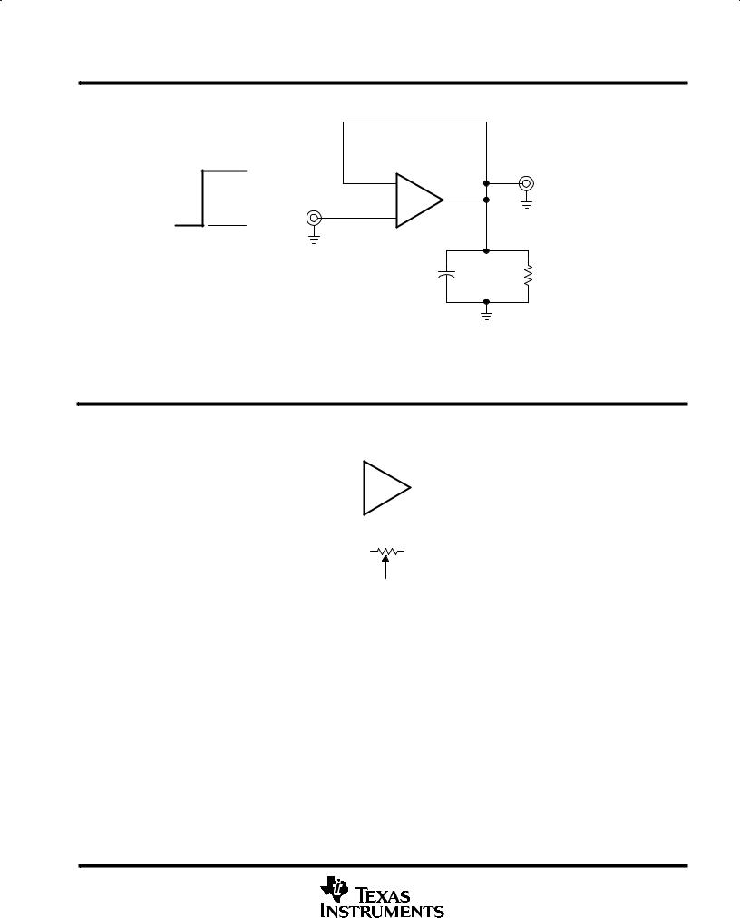
PARAMETER MEASUREMENT INFORMATION
VI
± |
OUT |
IN
+
0 V
INPUT VOLTAGE
WAVEFDORM
CL = 100 pF |
RL = 2 kΩ |
|
TEST CIRCUIT |
Figure 1. Rise Time, Overshoot, and Slew Rate
APPLICATION INFORMATION
Figure 2 shows a diagram for an input offset voltage null circuit.
IN + |
|
+ |
|
|
|
|
|
OUT |
|
|
|
|
|
|
|
||||
|
|
|
|
|
|
|
|
|
|
|
|
|
|
|
|
|
|
|
|
IN ± |
|
± |
|
|
|
OFFSET N2 |
|||
|
|
|
|
||||||
OFFSET N1 |
|
|
|
|
|
|
|
|
|
|
|
|
|
10 kΩ |
|
|
|
||
|
|
|
|
|
|
|
|
|
|
To VCC ±
Figure 2. Input Offset Voltage Null Circuit
POST OFFICE BOX 655303 •DALLAS, TEXAS 75265 |
7 |
 Loading...