


Texas Instruments THS1408CPFB, THS1403IPFB, THS1403QPFB, THS1403CPFB, THS1401QPFB Datasheet
...THS1401, THS1403, THS1408 14-BIT, 1/3/8 MSPS DSP COMPATIBLE ANALOG-TO-DIGITAL CONVERTERS WITH INTERNAL REFERENCE AND PGA
SLAS248 ± DECEMBER 1999
features |
applications |
D D D D D D
D D
D D D D
14-Bit Resolution |
D |
xDSL Front Ends |
1, 3, and 8 MSPS Speed Grades Available |
D |
Communication |
Differential Nonlinearity (DNL) ±0.6 LSB Typ |
D |
Industrial Control |
Integral Nonlinearity (INL) ±1.5 LSB Typ |
D |
Instrumentation |
Internal Reference |
|
|
Differential Inputs |
|
|
Programmable Gain Amplifier |
|
|
P Compatible Parallel Interface |
|
|
Timing Compatible With TMS320C6000 DSP |
|
|
3.3-V Single Supply |
|
|
Power-Down Mode |
|
|
Monolithic CMOS Design |
|
|
PFB PACKAGE (TOP VIEW)
|
|
|
|
|
IN+ |
|
AV |
AGND |
AGND AGND |
AV |
DV |
A0 |
A1 NC |
NC |
CS |
|
|
|
||||||||||||||||
|
|
|
|
|
|
|
DD |
|
|
|
|
|
|
DD |
DD |
|
|
|
|
|
|
|
|
|
|
|
|
|
|
|
|
|||
|
|
|
|
|
|
|
|
|
|
|
|
|
|
|
|
|
|
|
|
|
|
|
|
|
|
|
|
|
|
|
|
|
|
|
|
|
|
|
|
|
|
|
|
|
|
|
|
|
|
|
|
|
|
|
|
|
|
|
|
|
|
|
|
|
|
|
|
|
|
|
|
|
|
|
|
|
|
|
|
|
|
|
|
|
|
|
|
|
|
|
|
|
|
|
|
|
|
|
|
|
|
|
|
|
|
|
48 47 46 45 44 43 42 41 40 39 38 37 |
|
|
|
|
|
|
|
|
||||||||||||||||||||||||
|
|
|
|
|
|
|
|
|
||||||||||||||||||||||||||
|
|
|
|
|
|
|
|
|
|
|
|
|
|
|
|
|
|
|
|
|
|
|
|
|
|
|
|
|
|
|
|
|
|
|
IN± |
|
1 |
|
|
|
|
|
|
|
|
|
|
|
|
|
|
|
|
|
|
|
|
|
36 |
|
|
WR |
|
||||||
|
|
|
|
|
|
|
|
|
|
|
|
|
|
|
|
|
|
|
|
|
|
|
|
|
||||||||||
|
|
|
|
|
|
|
|
|
|
|
|
|
|
|
|
|
|
|
|
|
|
|
|
|
|
|
|
|
|
|
|
|
|
|
AVDD |
|
2 |
|
|
|
|
|
|
|
|
|
|
|
|
|
|
|
|
|
|
|
|
|
35 |
|
|
OE |
|
|
|||||
|
|
|
|
|
|
|
|
|
|
|
|
|
|
|
|
|
|
|
|
|
|
|
|
|
|
|
|
DGND |
||||||
VBG |
|
3 |
|
|
|
|
|
|
|
|
|
|
|
|
|
|
|
|
|
|
|
|
|
34 |
|
|
||||||||
|
|
|
|
|
|
|
|
|
|
|
|
|
|
|
|
|
|
|
|
|
|
|
|
|
|
|
DGND |
|||||||
CML |
|
4 |
|
|
|
|
|
|
|
|
|
|
|
|
|
|
|
|
|
|
|
|
|
33 |
|
|
||||||||
|
|
|
|
|
|
|
|
|
|
|
|
|
|
|
|
|
|
|
|
|
|
|
|
|
|
|
CLK |
|||||||
REF+ |
|
5 |
|
|
|
|
|
|
|
|
|
|
|
|
|
|
|
|
|
|
|
|
|
32 |
|
|
||||||||
|
|
|
|
|
|
|
|
|
|
|
|
|
|
|
|
|
|
|
|
|
|
|
|
|
|
|
DVDD |
|||||||
REF± |
|
6 |
|
|
|
|
|
|
|
|
|
|
|
|
|
|
|
|
|
|
|
|
|
31 |
|
|
||||||||
|
|
|
|
|
|
|
|
|
|
|
|
|
|
|
|
|
|
|
|
|
|
|
|
|
|
|
DVDD |
|||||||
AGND |
|
7 |
|
|
|
|
|
|
|
|
|
|
|
|
|
|
|
|
|
|
|
|
|
30 |
|
|
||||||||
|
|
|
|
|
|
|
|
|
|
|
|
|
|
|
|
|
|
|
|
|
|
|
|
|
|
|
D0 |
|||||||
AGND |
|
8 |
|
|
|
|
|
|
|
|
|
|
|
|
|
|
|
|
|
|
|
|
|
29 |
|
|
||||||||
|
|
|
|
|
|
|
|
|
|
|
|
|
|
|
|
|
|
|
|
|
|
|
|
|
|
|
D1 |
|||||||
DGND |
|
9 |
|
|
|
|
|
|
|
|
|
|
|
|
|
|
|
|
|
|
|
|
|
28 |
|
|
||||||||
|
|
|
|
|
|
|
|
|
|
|
|
|
|
|
|
|
|
|
|
|
|
|
|
|
|
|
D2 |
|||||||
OV |
|
10 |
|
|
|
|
|
|
|
|
|
|
|
|
|
|
|
|
|
|
|
|
|
27 |
|
|
||||||||
D13 |
|
11 |
|
|
|
|
|
|
|
|
|
|
|
|
|
|
|
|
|
|
|
|
|
26 |
|
|
DVDD |
|||||||
|
|
|
|
|
|
|
|
|
|
|
|
|
|
|
|
|
|
|
|
|
|
|
|
|||||||||||
D12 |
|
12 |
|
|
|
|
|
|
|
|
|
|
|
|
|
|
|
|
|
|
|
|
|
25 |
|
|
DGND |
|||||||
|
|
|
|
|
|
|
|
|
|
|
|
|
|
|
|
|
|
|
|
|
|
|
|
|||||||||||
|
|
|
13 |
14 15 16 17 18 19 |
|
20 21 22 23 24 |
|
|
|
|
|
|
|
|
||||||||||||||||||||
|
|
|
|
|
|
|
|
|
||||||||||||||||||||||||||
|
|
|
|
|
|
|
|
|
|
|
|
|
|
|
|
|
|
|
|
|
|
|
|
|
|
|
|
|
|
|
|
|
||
|
|
|
|
|
D11 |
|
DV |
DGND |
D10 D9 |
D8 |
D7 |
DV |
D6 D5 |
D4 |
D3 |
|
|
|
||||||||||||||||
|
|
|
|
|
|
|
DD |
|
|
|
|
|
|
|
|
|
|
DD |
|
|
|
|
|
|
|
|
|
|
|
|
|
|
||
NC ± No internal connection
Please be aware that an important notice concerning availability, standard warranty, and use in critical applications of Texas Instruments semiconductor products and disclaimers thereto appears at the end of this data sheet.
PRODUCTION DATA information is current as of publication date. Products conform to specifications per the terms of Texas Instruments standard warranty. Production processing does not necessarily include testing of all parameters.
Copyright 1999, Texas Instruments Incorporated
POST OFFICE BOX 655303 •DALLAS, TEXAS 75265 |
1 |

THS1401, THS1403, THS1408
14-BIT, 1/3/8 MSPS DSP COMPATIBLE ANALOG-TO-DIGITAL CONVERTERS WITH INTERNAL REFERENCE AND PGA
SLAS248 ± DECEMBER 1999
description
The THS1401, THS1403, and THS1408 are 14-bit, 1/3/8 MSPS, single supply analog-to-digital converters with an internal reference, differential inputs, programmable input gain, and an on-chip sample and hold amplifier.
Implemented with a CMOS process, the device has outstanding price/performance and power/speed ratios. The THS1401, THS1403, and THS1408 are designed for use with 3.3-V systems, and with a high-speed P compatible parallel interface, making them the first choice for solutions based on high-performance DSPs like the TI TMS320C6000 series.
The THS1401, THS1403, and THS1408 are available in a TQFP-48 package in standard commercial and industrial temperature ranges.
functional block diagram
VBG |
|
|
|
REF+ |
|
REF |
|
|
|
1.5 V |
|
|
|
REF± |
|
|
|
|
|
BG |
|
|
|
|
IN+ |
|
14 |
|
15 |
PGA |
14-Bit |
|
||
|
Buffer |
D[13:0] + OV bit |
||
0..7 dB |
ADC |
|
||
|
|
|||
|
|
|
||
IN± |
|
|
|
|
6 |
|
|
|
|
|
|
A[1:0] |
CLK |
CONTROL |
CS |
|
LOGIC |
WR |
|
|
OE |
AVAILABLE OPTIONS
|
PACKAGED DEVICE |
TA |
|
TQFP |
|
|
(PFB) |
|
|
|
THS1401CPFB, |
0°C to 70°C |
THS1403CPFB, |
|
THS1408CPFB, |
|
|
|
THS1401IPFB, |
±40°C to 85°C |
THS1403IPFB, |
|
THS1408IPFB |
2 |
POST OFFICE BOX 655303 •DALLAS, TEXAS 75265 |

THS1401, THS1403, THS1408 14-BIT, 1/3/8 MSPS DSP COMPATIBLE ANALOG-TO-DIGITAL CONVERTERS WITH INTERNAL REFERENCE AND PGA
SLAS248 ± DECEMBER 1999
|
|
|
|
|
|
|
Terminal Functions |
|
|
|
|
|
|
|
|
|
|
|
|
TERMINAL |
I/O |
DESCRIPTION |
|
|
NAME |
NO. |
|||||
|
|
|
|||||
|
|
|
|
|
|
|
|
|
A[1:0] |
40, 41 |
I |
Address input |
|||
|
|
|
|
|
|
|
|
|
AGND |
7,8, 44, |
P |
Analog ground |
|||
|
|
|
|
|
45, 46 |
|
|
|
|
|
|
|
|
|
|
|
AVDD |
2, 43, 47 |
P |
Analog power supply |
|||
|
CLK |
32 |
I |
Clock input |
|||
|
|
|
|
|
|
|
|
|
CML |
4 |
|
Reference midpoint. This pin requires a 0.1- F capacitor to AGND. |
|||
|
|
|
|
|
|
|
|
|
|
|
|
|
37 |
I |
Chip select input. Active low |
|
CS |
|
|
|
|||
|
|
|
|
|
|
|
|
|
DGND |
9, 15, 25, |
P |
Digital ground |
|||
|
|
|
|
|
33, 34 |
|
|
|
|
|
|
|
|
|
|
|
DVDD |
14, 20, 26, |
P |
Digital power supply |
|||
|
|
|
|
|
30, 31, 42 |
|
|
|
|
|
|
|
|
|
|
|
D[13:0] |
11, 12, 13, |
I/O |
Data inputs/outputs |
|||
|
|
|
|
|
16, 17, 18, |
|
|
|
|
|
|
|
19,21, 22, |
|
|
|
|
|
|
|
23, 24, 27, |
|
|
|
|
|
|
|
28, 29 |
|
|
|
|
|
|
|
|
|
|
|
NC |
38, 39 |
|
No connection, do not use. Reserved |
|||
|
|
|
|
|
|
|
|
|
IN+ |
48 |
I |
Positive differential analog input |
|||
|
|
|
|
|
|
|
|
|
IN± |
1 |
I |
Negative differential analog input |
|||
|
|
|
|
|
|
||
|
|
|
|
|
35 |
I |
Output enable. Active low |
|
OE |
|
|
||||
|
|
|
|
|
|
||
|
OV |
10 |
O |
Out of range output |
|||
|
|
|
|
|
|
||
|
REF+ |
5 |
O |
Positive reference output. This pin requires a 0.1- F capacitor to AGND. |
|||
|
|
|
|
|
|
||
|
REF± |
6 |
O |
Negative reference output. This pin requires a 0.1- F capacitor to AGND. |
|||
|
|
|
|
|
|
||
|
VBG |
3 |
I |
Reference input. This pin requires a 1- F capacitor to AGND. |
|||
|
|
|
|
|
|||
|
|
|
|
|
36 |
I |
Write signal. Active low |
|
WR |
|
|||||
|
|
|
|
|
|
|
|
absolute maximum ratings over operating free-air temperature (unless otherwise noted)²
Supply voltage, (AVDD to AGND) . . . . . . . . . . . . . . . . . . . . . . . . . . . . . . . . . . . . . . . . . . . |
. . . . . . . . . . . . . . . . . . 4V |
|
Supply voltage, (DVDD to DGND) . . . . . . . . . . . . . . . . . . . . . . . . . . . . . . . . . . . . . . . . . . . . |
. . . . . . . . . . . . . . . . . 4V |
|
Reference input voltage range, VBG . . . . . . . . . . . . . . . . . . . . . . . . . . . . . . . . . . . . . . . |
± 0.3 V to AVDD + 0.3 |
V |
Analog input voltage range . . . . . . . . . . . . . . . . . . . . . . . . . . . . . . . . . . . . . . . . . . . . . . . . . |
± 0.3 V to AVDD + 0.3 |
V |
Digital input voltage range . . . . . . . . . . . . . . . . . . . . . . . . . . . . . . . . . . . . . . . . . . . . . . . . . |
± 0.3 V to DVDD + 0.3 |
V |
Operating free-air temperature range, TA: C suffix . . . . . . . . . . . . . . . . . . . . . . . . . . . . . |
. . . . . . . . . 0°C to 70°C |
|
I suffix . . . . . . . . . . . . . . . . . . . . . . . . . . . . . . |
. . . . . . . ±40°C to 85°C |
|
Storage temperature range, Tstg . . . . . . . . . . . . . . . . . . . . . . . . . . . . . . . . . . . . . . . . . . . . . |
. . . . . ±65°C to 150°C |
|
Lead temperature 1.6 mm (1/16 inch) from case for 10 seconds . . . . . . . . . . . . . . . . . . |
. . . . . . . . . . . . . . 260°C |
|
²Stresses beyond those listed under ªabsolute maximum ratingsº may cause permanent damage to the device. These are stress ratings only, and functional operation of the device at these or any other conditions beyond those indicated under ªrecommended operating conditionsº is not implied. Exposure to absolute-maximum-rated conditions for extended periods may affect device reliability.
POST OFFICE BOX 655303 •DALLAS, TEXAS 75265 |
3 |

THS1401, THS1403, THS1408
14-BIT, 1/3/8 MSPS DSP COMPATIBLE ANALOG-TO-DIGITAL CONVERTERS WITH INTERNAL REFERENCE AND PGA
SLAS248 ± DECEMBER 1999
recommended operating conditions
|
PARAMETER |
MIN |
NOM |
MAX |
UNIT |
|
|
|
|
|
|
|
|
Supply voltage, AVDD, DVDD |
|
|
3 |
3.3 |
3.6 |
V |
High level digital input, VIH |
|
|
2 |
3.3 |
|
V |
Low level digital input, VIL |
|
|
|
0 |
0.8 |
V |
Load capacitance, CL |
|
|
|
5 |
15 |
pF |
|
|
THS1401 |
0.1 |
1 |
1 |
MHz |
Clock frequency, fCLK |
|
|
|
|
|
|
|
THS1403 |
0.1 |
3 |
3 |
MHz |
|
|
|
THS1408 |
0.1 |
8 |
8 |
MHz |
|
|
|
|
|
|
|
Clock duty cycle |
|
|
40% |
50% |
60% |
|
|
|
|
|
|
|
|
Operating free-air temperature |
|
C suffix |
0 |
25 |
70 |
°C |
|
|
|
|
|
|
|
|
I suffix |
±40 |
25 |
85 |
°C |
|
|
|
|||||
electrical characteristics over recommended operating conditions
|
PARAMETER |
|
TEST CONDITIONS |
MIN |
TYP |
MAX |
UNIT |
|
|
|
|
|
|
|
|
Power Supply |
|
|
|
|
|
|
|
|
|
|
|
|
|
|
|
IDDA |
Analog supply current |
|
|
|
81 |
90 |
mA |
IDDD |
Digital supply current |
|
|
|
5 |
10 |
mA |
|
Power |
|
|
|
270 |
360 |
mW |
|
|
|
|
|
|
|
|
|
Power down current |
|
|
|
20 |
|
A |
|
|
|
|
|
|
|
|
DC Characteristics |
|
|
|
|
|
|
|
|
|
|
|
|
|
|
|
|
Resolution |
|
|
|
14 |
|
Bits |
|
|
|
|
|
|
|
|
DNL |
Differential nonlinearity |
|
|
|
±0.6 |
±1 |
LSB |
|
|
|
|
|
|
|
|
|
|
THS1401 |
|
|
±1.5 |
±2.5 |
LSB |
|
|
|
|
|
|
|
|
INL |
Integral nonlinearity |
THS1403 |
Best fit |
|
±1.5 |
±2.5 |
LSB |
|
|
|
|
|
|
|
|
|
|
THS1408 |
|
|
±3 |
±5 |
LSB |
|
|
|
|
|
|
|
|
|
Offset error |
|
IN+ = IN±, PGA = 0 dB |
|
|
0.3 |
%FSR |
|
|
|
|
|
|
|
|
|
Gain error |
|
PGA = 0 dB |
|
|
1 |
%FSR |
|
|
|
|
|
|
|
|
AC Characteristics |
|
|
|
|
|
|
|
|
|
|
|
|
|
|
|
ENOB |
Effective number of bits |
|
|
11.2 |
11.5 |
|
Bits |
|
|
|
|
|
|
|
|
|
|
THS1401/3/8 |
fi = 100 kHz |
|
±81 |
|
|
THD |
Total harmonic distortion |
THS1403/8 |
fi = 1 MHz |
|
±78 |
|
dB |
|
|
THS1408 |
fi = 4 MHz |
|
±77 |
|
|
|
|
THS1401/3/8 |
fi = 100 kHz |
|
72 |
|
|
SNR |
Signal-to-noise ratio |
THS1403/8 |
fi = 1 MHz |
70 |
72 |
|
dB |
|
|
THS1408 |
fi = 4 MHz |
|
71 |
|
|
|
|
THS1401/3/8 |
fi = 100 kHz |
|
70 |
|
|
SINAD |
Signal-to-noise ratio + distortion |
THS1403/8 |
fi = 1 MHz |
69 |
70 |
|
dB |
|
|
THS1408 |
fi = 4 MHz |
|
70 |
|
|
|
|
THS1401/3/8 |
fi = 100 kHz |
|
80 |
|
|
SFDR |
Spurious free dynamic range |
THS1403/8 |
fi = 1 MHz |
73 |
80 |
|
dB |
|
|
THS1408 |
fi = 4 MHz |
|
80 |
|
|
|
Analog input bandwidth |
|
|
|
140 |
|
MHz |
4 |
POST OFFICE BOX 655303 •DALLAS, TEXAS 75265 |

THS1401, THS1403, THS1408 14-BIT, 1/3/8 MSPS DSP COMPATIBLE ANALOG-TO-DIGITAL CONVERTERS WITH INTERNAL REFERENCE AND PGA
SLAS248 ± DECEMBER 1999
electrical characteristics (continued)
|
|
PARAMETER |
TEST CONDITIONS |
MIN |
TYP |
MAX |
UNIT |
|
|
|
|
|
|
|
|
Reference Voltage |
|
|
|
|
|
||
|
|
|
|
|
|
|
|
VBG |
|
Bandgap voltage, internal mode |
|
1.425 |
1.5 |
1.575 |
V |
|
|
|
|
|
|
|
|
|
Input impedance |
|
|
40 |
|
kΩ |
|
|
|
|
|
|
|||
|
|
|
|
|
|
|
|
|
|
Positive reference voltage, REF+ |
|
|
2.5 |
|
V |
|
|
|
|
|
|
|
|
|
|
Negative reference voltage, REF± |
|
|
0.5 |
|
V |
|
|
|
|
|
|
|
|
|
|
Reference difference, REF, REF+ ± REF± |
|
|
2 |
|
V |
|
|
|
|
|
|
|
|
|
|
Accuracy, internal reference |
|
|
5% |
|
|
|
|
|
|
|
|
|
|
|
|
Temperature coefficient |
|
|
40 |
|
ppm/°C |
|
|
|
|
|
|
|
|
|
|
Voltage coefficient |
|
|
200 |
|
ppm/V |
|
|
|
|
|
|
|
|
Analog Inputs |
|
|
|
|
|
|
|
|
|
|
|
|
|
|
|
|
|
Positive analog input, IN+ |
|
0 |
|
AVDD |
V |
|
|
Negative analog input, IN± |
|
0 |
|
AVDD |
V |
|
|
Analog input voltage difference |
Ain = IN+ ± IN±, Vref = REF+ ± REF± |
±Vref |
|
Vref |
V |
|
|
Input impedance |
|
|
25 |
|
kΩ |
|
|
PGA range |
|
0 |
|
7 |
dB |
|
|
|
|
|
|
|
|
|
|
PGA step size |
|
|
1 |
|
dB |
|
|
|
|
|
|
|
|
|
|
PGA gain error |
|
|
|
±0.25 |
dB |
|
|
|
|
|
|
|
|
Digital Inputs |
|
|
|
|
|
|
|
|
|
|
|
|
|
|
|
VIH |
High-level digital input |
|
2 |
|
|
V |
|
VIL |
Low-level digital input |
|
|
|
0.8 |
V |
|
|
|
Input capacitance |
|
|
5 |
|
pF |
|
|
|
|
|
|
|
|
|
|
Input current |
|
|
|
±1 |
µA |
|
|
|
|
|
|
|
|
Digital Outputs |
|
|
|
|
|
|
|
|
|
|
|
|
|
|
|
VOH |
High-level digital output |
IOH = 50 µA |
2.6 |
|
|
V |
|
VOL |
Low-level digital output |
IOL = 50 µA |
|
|
0.4 |
V |
|
IOZ |
Output current, high impedance |
|
|
|
±10 |
µA |
|
Clock Timing (CS low) |
|
|
|
|
|
||
|
|
|
|
|
|
|
|
|
|
|
THS1401 |
0.1 |
1 |
1 |
MHz |
fCLK |
Clock frequency |
|
|
|
|
|
|
THS1403 |
0.1 |
3 |
3 |
MHz |
|||
|
|
|
THS1408 |
0.1 |
8 |
8 |
MHz |
|
|
|
|
|
|
|
|
td |
Output delay time |
|
|
|
25 |
ns |
|
|
|
Latency |
|
|
9.5 |
|
Cycles |
POST OFFICE BOX 655303 •DALLAS, TEXAS 75265 |
5 |
THS1401, THS1403, THS1408
14-BIT, 1/3/8 MSPS DSP COMPATIBLE ANALOG-TO-DIGITAL CONVERTERS WITH INTERNAL REFERENCE AND PGA
SLAS248 ± DECEMBER 1999
PARAMETER MEASUREMENT INFORMATION
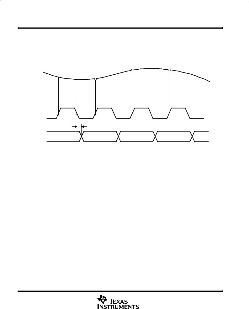
sample timing
The THS1401/3/8 core is based on a pipeline architecture with a latency of 9.5 samples. The conversion results appear on the digital output 9.5 clock cycles after the input signal was sampled.
S11 |
S12 |
|
S9
Analog  S10
S10
Input
tw(CLK)  tw(CLK)
CLK |
|
|
|
|
td |
|
|
Data |
C1 |
C2 |
C3 |
|
Out
Figure 1. Sample Timing
The parallel interface of the THS1401/3/8 ADC features 3-state buffers making it possible to directly connect it to a data bus. The output buffers are enabled by driving the OE input low.
Besides the sample results, it is also possible to read back the values of the control register, the PGA register, and the control register. Which register is read is determined by the address inputs A[1,0]. The ADC results are available at address 0.
The timing of the control signals is described in the following sections.
6 |
POST OFFICE BOX 655303 •DALLAS, TEXAS 75265 |
THS1401, THS1403, THS1408 14-BIT, 1/3/8 MSPS DSP COMPATIBLE ANALOG-TO-DIGITAL CONVERTERS WITH INTERNAL REFERENCE AND PGA
SLAS248 ± DECEMBER 1999
PARAMETER MEASUREMENT INFORMATION
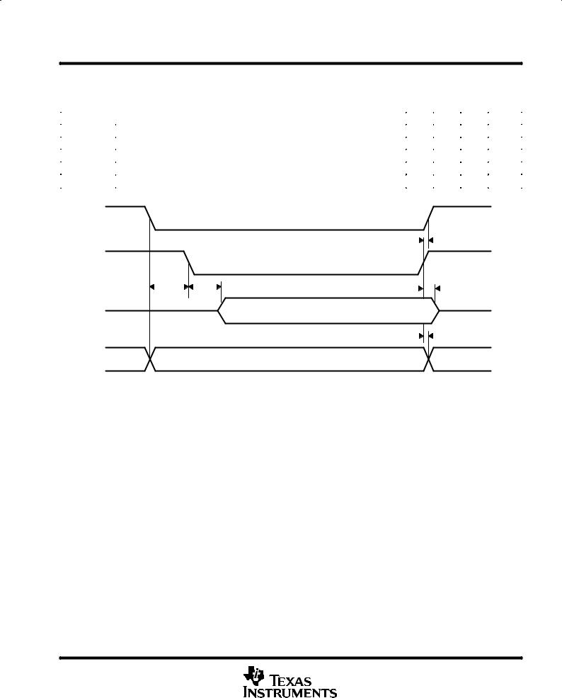
read timing (15-pF load)
|
|
|
|
|
|
|
|
|
|
|
|
PARAMETER |
|
|
MIN |
TYP MAX |
UNIT |
|||||||||||||||||
|
|
|
|
|
|
|
|
|
|
|
|
|
|
|
|
|
|
|
|
|
|
|
|
|
|
|
|
|
|
|
|
|
|
|
tsu(OE±ACS) |
Address and chip select setup time |
|
4 |
|
|
|
|
|
|
ns |
||||||||||||||||||||||||
ten |
Output enable |
|
|
|
|
|
|
|
|
|
|
|
|
|
|
|
|
|
|
|
|
15 |
ns |
|||||||||||
tdis |
Output disable |
|
|
|
|
|
|
|
|
|
|
|
|
|
|
|
|
|
|
|
|
10 |
ns |
|||||||||||
th(A) |
Address hold time |
|
|
|
|
|
|
|
1 |
|
|
|
|
15 |
ns |
|||||||||||||||||||
th(CS) |
Chip select hold time |
|
|
|
|
|
|
|
0 |
|
|
|
|
|
|
ns |
||||||||||||||||||
NOTE: All timing parameters refer to a 50% level. |
|
|
|
|
|
|
|
|
|
|
|
|
|
|
|
|
|
|||||||||||||||||
|
|
|
|
|
|
|
|
|
|
|
|
|
|
|
|
|
|
|
|
|
|
|
|
|
|
|
|
|
|
|
|
|
|
|
|
CS |
|
|
|
|
|
|
|
|
|
|
|
|
|
|
|
|
|
|
|
|
|
|
|
|
|
|
|
|
|
|
th(CS) |
|
|
|
|
|
|
|
|
|
|
|
|
|
|
|
|
|
|
|
|
|
|
|
|
|
|
|
|
|
|
|
|
|
|
|
||
|
|
|
|
|
|
|
|
|
|
|
|
|
|
|
|
|
|
|
|
|
|
|
|
|
|
|
|
|
|
|
|
|
||
|
|
|
|
|
|
|
|
|
|
|
|
|
|
|
|
|
|
|
|
|
|
|
|
|
|
|
|
|
|
|
|
|
|
|
|
OE |
|
|
|
|
|
|
|
|
|
|
|
|
|
|
|
|
|
|
|
|
|
|
|
|
|
|
|
|
|
|
|
|
|
|
tsu(OE±ACS) |
|
|
|
|
|
|
|
|
|
|
|
|
|
ten |
|
|
|
|
|
|
|
|
|
|
|
|
|
|
|
tdis |
|
||
|
|
|
|
|
|
|
|
|
|
|
|
|
|
|
|
|
|
|
|
|
|
|
|
|
|
|
|
|||||||
|
|
|
|
|
|
|
|
|
|
|
|
|
|
|
|
|
|
|
|
|
|
|
|
|
|
|
|
|
|
|||||
|
|
|
|
|
|
|
|
|
|
|
|
|
|
|
|
|
|
|
|
|
|
|
|
|
|
|
|
|
|
|
|
|||
D[13:0] |
|
|
|
|
|
|
|
|
|
|
|
|
|
|
|
DATA |
|
|
|
|
|
|||||||||||||
O V |
|
|
|
|
|
|
|
|
|
|
|
|
|
|
|
|
|
|
|
|
|
|
|
|
|
|
|
|
|
|
|
|
||
A[1:0] |
|
|
|
|
|
|
|
|
|
|
|
|
|
|
|
|
|
|
|
|
|
|
|
|
|
|
|
|
|
th(A) |
|
|||
|
|
|
|
|
|
|
|
|
|
|
|
|
|
|
|
|
|
|
|
|
|
|
|
|
|
|
|
|
|
|||||
X |
|
|
|
|
|
|
|
|
|
|
|
|
|
ADDRESS |
|
|
|
|
|
|
|
X |
|
|||||||||||
|
|
|
|
|
|
|
|
|
|
|
|
|
|
|
|
|
|
|||||||||||||||||
Figure 2. Read Timing
POST OFFICE BOX 655303 •DALLAS, TEXAS 75265 |
7 |
 Loading...