


 Loading...
Texas Instruments TMS320F28016, TMS320C2802, TMS320F2808, TMS320F2809, TMS320F28015 User Manual
...TMS320F2809, TMS320F2808, TMS320F2806 TMS320F2802, TMS320F2801, TMS320C2802 TMS320C2801, TMS320F28016, TMS320F28015
Digital Signal Processors
Data Manual
PRODUCTION DATA information is current as of publication date. Products conform to specifications per the terms of the Texas Instruments standard warranty. Production processing does not necessarily include testing of all parameters.
Literature Number: SPRS230L
October 2003–Revised December 2009

TMS320F2809, TMS320F2808, TMS320F2806
TMS320F2802, TMS320F2801, TMS320C2802
TMS320C2801, TMS320F28016, TMS320F28015
SPRS230L –OCTOBER 2003 –REVISED DECEMBER 2009 www.ti.com
|
|
|
Contents |
|
1 |
F280x, F2801x, C280x DSPs .................................................................................................. |
9 |
||
|
1.1 |
Features |
...................................................................................................................... |
9 |
|
1.2 |
Getting Started ............................................................................................................. |
10 |
|
2 |
Introduction ...................................................................................................................... |
|
11 |
|
|
2.1 |
Pin Assignments ........................................................................................................... |
14 |
|
|
2.2 |
Signal Descriptions ........................................................................................................ |
19 |
|
3 |
Functional Overview .......................................................................................................... |
25 |
||
|
3.1 |
Memory Maps .............................................................................................................. |
26 |
|
|
3.2 |
Brief Descriptions .......................................................................................................... |
34 |
|
|
|
3.2.1 |
C28x CPU ....................................................................................................... |
34 |
|
|
3.2.2 |
Memory Bus (Harvard Bus Architecture) .................................................................... |
34 |
|
|
3.2.3 |
Peripheral Bus .................................................................................................. |
34 |
|
|
3.2.4 |
Real-Time JTAG and Analysis ................................................................................ |
35 |
|
|
3.2.5 |
Flash ............................................................................................................. |
35 |
|
|
3.2.6 |
ROM .............................................................................................................. |
35 |
|
|
3.2.7 |
M0, M1 SARAMs ............................................................................................... |
35 |
|
|
3.2.8 |
L0, L1, H0 SARAMs ............................................................................................ |
36 |
|
|
3.2.9 |
Boot ROM ....................................................................................................... |
36 |
|
|
3.2.10 |
Security .......................................................................................................... |
37 |
|
|
3.2.11 |
Peripheral Interrupt Expansion (PIE) Block ................................................................. |
38 |
|
|
3.2.12 |
External Interrupts (XINT1, XINT2, XNMI) .................................................................. |
38 |
|
|
3.2.13 |
Oscillator and PLL .............................................................................................. |
38 |
|
|
3.2.14 |
Watchdog ........................................................................................................ |
38 |
|
|
3.2.15 |
Peripheral Clocking ............................................................................................. |
38 |
|
|
3.2.16 |
Low-Power Modes .............................................................................................. |
38 |
|
|
3.2.17 |
Peripheral Frames 0, 1, 2 (PFn) .............................................................................. |
39 |
|
|
3.2.18 |
General-Purpose Input/Output (GPIO) Multiplexer ......................................................... |
39 |
|
|
3.2.19 |
32-Bit CPU-Timers (0, 1, 2) ................................................................................... |
39 |
|
|
3.2.20 |
Control Peripherals ............................................................................................. |
39 |
|
|
3.2.21 |
Serial Port Peripherals ......................................................................................... |
40 |
|
3.3 |
Register Map ............................................................................................................... |
40 |
|
|
3.4 |
Device Emulation Registers .............................................................................................. |
42 |
|
|
3.5 |
Interrupts .................................................................................................................... |
42 |
|
|
|
3.5.1 |
External Interrupts .............................................................................................. |
45 |
|
3.6 |
System Control ............................................................................................................ |
46 |
|
|
|
3.6.1 |
OSC and PLL Block ............................................................................................ |
47 |
|
|
|
3.6.1.1 External Reference Oscillator Clock Option .................................................... |
48 |
|
|
|
3.6.1.2 PLL-Based Clock Module ......................................................................... |
49 |
|
|
|
3.6.1.3 Loss of Input Clock ................................................................................ |
50 |
|
|
3.6.2 |
Watchdog Block ................................................................................................. |
51 |
|
3.7 |
Low-Power Modes Block ................................................................................................. |
52 |
|
4 |
Peripherals ....................................................................................................................... |
|
53 |
|
|
4.1 |
32-Bit CPU-Timers 0/1/2 ................................................................................................. |
53 |
|
|
4.2 |
Enhanced PWM Modules (ePWM1/2/3/4/5/6) ......................................................................... |
55 |
|
|
4.3 |
Hi-Resolution PWM (HRPWM) .......................................................................................... |
58 |
|
2 |
Contents |
Copyright © 2003–2009, Texas Instruments Incorporated |

TMS320F2809, TMS320F2808, TMS320F2806
TMS320F2802, TMS320F2801, TMS320C2802
TMS320C2801, TMS320F28016, TMS320F28015
www.ti.com |
|
SPRS230L –OCTOBER 2003 –REVISED DECEMBER 2009 |
||
|
4.4 |
Enhanced CAP Modules (eCAP1/2/3/4) ................................................................................ |
58 |
|
|
4.5 |
Enhanced QEP Modules (eQEP1/2) .................................................................................... |
61 |
|
|
4.6 |
Enhanced Analog-to-Digital Converter (ADC) Module ............................................................... |
63 |
|
|
|
4.6.1 |
ADC Connections if the ADC Is Not Used .................................................................. |
66 |
|
|
4.6.2 |
ADC Registers .................................................................................................. |
67 |
|
4.7 |
Enhanced Controller Area Network (eCAN) Modules (eCAN-A and eCAN-B) .................................... |
68 |
|
|
4.8 |
Serial Communications Interface (SCI) Modules (SCI-A, SCI-B) ................................................... |
73 |
|
|
4.9 |
Serial Peripheral Interface (SPI) Modules (SPI-A, SPI-B, SPI-C, SPI-D) .......................................... |
76 |
|
|
4.10 |
Inter-Integrated Circuit (I2C) ............................................................................................. |
80 |
|
|
4.11 |
GPIO MUX ................................................................................................................. |
82 |
|
5 |
Device Support ................................................................................................................. |
86 |
||
|
5.1 |
Device and Development Support Tool Nomenclature ............................................................... |
86 |
|
|
5.2 |
Documentation Support ................................................................................................... |
88 |
|
6 |
Electrical Specifications ..................................................................................................... |
93 |
||
|
6.1 |
Absolute Maximum Ratings .............................................................................................. |
93 |
|
|
6.2 |
Recommended Operating Conditions .................................................................................. |
94 |
|
|
6.3 |
Electrical Characteristics ................................................................................................. |
94 |
|
|
6.4 |
Current Consumption ..................................................................................................... |
95 |
|
|
|
6.4.1 |
Reducing Current Consumption .............................................................................. |
99 |
|
|
6.4.2 |
Current Consumption Graphs ............................................................................... |
100 |
|
6.5 |
Emulator Connection Without Signal Buffering for the DSP ....................................................... |
102 |
|
|
6.6 |
Timing Parameter Symbology .......................................................................................... |
103 |
|
|
|
6.6.1 |
General Notes on Timing Parameters ...................................................................... |
103 |
|
|
6.6.2 |
Test Load Circuit .............................................................................................. |
103 |
|
|
6.6.3 |
Device Clock Table ........................................................................................... |
104 |
|
6.7 |
Clock Requirements and Characteristics ............................................................................. |
105 |
|
|
6.8 |
Power Sequencing ....................................................................................................... |
106 |
|
|
|
6.8.1 |
Power Management and Supervisory Circuit Solutions .................................................. |
106 |
|
6.9 |
General-Purpose Input/Output (GPIO) ................................................................................ |
109 |
|
|
|
6.9.1 |
GPIO - Output Timing ........................................................................................ |
109 |
|
|
6.9.2 |
GPIO - Input Timing .......................................................................................... |
110 |
|
|
6.9.3 |
Sampling Window Width for Input Signals ................................................................. |
111 |
|
|
6.9.4 |
Low-Power Mode Wakeup Timing .......................................................................... |
112 |
|
6.10 |
Enhanced Control Peripherals ......................................................................................... |
115 |
|
|
|
6.10.1 |
Enhanced Pulse Width Modulator (ePWM) Timing ....................................................... |
115 |
|
|
6.10.2 |
Trip-Zone Input Timing ....................................................................................... |
115 |
|
|
6.10.3 |
External Interrupt Timing ..................................................................................... |
117 |
|
|
6.10.4 |
I2C Electrical Specification and Timing .................................................................... |
118 |
|
|
6.10.5 |
Serial Peripheral Interface (SPI) Master Mode Timing ................................................... |
118 |
|
|
6.10.6 |
SPI Slave Mode Timing ...................................................................................... |
123 |
|
|
6.10.7 |
On-Chip Analog-to-Digital Converter ....................................................................... |
125 |
|
|
|
6.10.7.1 ADC Power-Up Control Bit Timing ............................................................. |
126 |
|
|
|
6.10.7.2 Definitions ......................................................................................... |
127 |
|
|
|
6.10.7.3 Sequential Sampling Mode (Single-Channel) (SMODE = 0) ............................... |
128 |
|
|
|
6.10.7.4 Simultaneous Sampling Mode (Dual-Channel) (SMODE = 1) .............................. |
129 |
|
6.11 |
Detailed Descriptions .................................................................................................... |
130 |
|
|
6.12 |
Flash Timing .............................................................................................................. |
131 |
|
Copyright © 2003–2009, Texas Instruments Incorporated |
Contents |
3 |

TMS320F2809, TMS320F2808, TMS320F2806
TMS320F2802, TMS320F2801, TMS320C2802
TMS320C2801, TMS320F28016, TMS320F28015
SPRS230L –OCTOBER 2003 –REVISED DECEMBER 2009 |
www.ti.com |
||
|
6.13 ROM Timing (C280x only) .............................................................................................. |
132 |
|
7 |
Migrating From F280x Devices to C280x Devices ................................................................. |
133 |
|
|
7.1 |
Migration Issues .......................................................................................................... |
133 |
8 |
Revision History .............................................................................................................. |
134 |
|
9 |
Mechanical Data .............................................................................................................. |
135 |
|
4 |
Contents |
Copyright © 2003–2009, Texas Instruments Incorporated |

TMS320F2809, TMS320F2808, TMS320F2806
TMS320F2802, TMS320F2801, TMS320C2802
TMS320C2801, TMS320F28016, TMS320F28015
www.ti.com SPRS230L –OCTOBER 2003 –REVISED DECEMBER 2009
List of Figures
2-1 |
TMS320F2809, TMS320F2808 100-Pin PZ LQFP (Top View) ............................................................ |
15 |
2-2 |
TMS320F2806 100-Pin PZ LQFP (Top View)................................................................................ |
16 |
2-3 |
TMS320F2802, TMS320F2801, TMS320C2802, TMS320C2801 100-Pin PZ LQFP (Top View) ..................... |
17 |
2-4 |
TMS320F2801x 100-Pin PZ LQFP (Top View) .............................................................................. |
18 |
2-5 |
TMS320F2809, TMS320F2808, TMS320F2806,TMS320F2802, TMS320F2801, |
|
|
TMS320F28016, TMS320F28015, TMS320C2802, TMS320C2801 |
|
|
100-Ball GGM and ZGM MicroStar BGA™ (Bottom View) ................................................................. |
18 |
3-1 |
Functional Block Diagram ....................................................................................................... |
26 |
3-2 |
F2809 Memory Map.............................................................................................................. |
27 |
3-3 |
F2808 Memory Map.............................................................................................................. |
28 |
3-4 |
F2806 Memory Map.............................................................................................................. |
29 |
3-5 |
F2802, C2802 Memory Map .................................................................................................... |
30 |
3-6 |
F2801, F28015, F28016, C2801 Memory Map............................................................................... |
30 |
3-7 |
External and PIE Interrupt Sources ............................................................................................ |
44 |
3-8 |
Multiplexing of Interrupts Using the PIE Block ............................................................................... |
44 |
3-9 |
Clock and Reset Domains ...................................................................................................... |
46 |
3-10 |
OSC and PLL Block Diagram................................................................................................... |
47 |
3-11 |
Using a 3.3-V External Oscillator............................................................................................... |
48 |
3-12 |
Using a 1.8-V External Oscillator............................................................................................... |
48 |
3-13 |
Using the Internal Oscillator .................................................................................................... |
48 |
3-14 |
Watchdog Module ................................................................................................................ |
51 |
4-1 |
CPU-Timers ....................................................................................................................... |
53 |
4-2 |
CPU-Timer Interrupt Signals and Output Signal ............................................................................. |
54 |
4-3 |
Multiple PWM Modules in a 280x System .................................................................................... |
55 |
4-4 |
ePWM Sub-Modules Showing Critical Internal Signal Interconnections .................................................. |
57 |
4-5 |
eCAP Functional Block Diagram ............................................................................................... |
59 |
4-6 |
eQEP Functional Block Diagram ............................................................................................... |
61 |
4-7 |
Block Diagram of the ADC Module ............................................................................................ |
64 |
4-8 |
ADC Pin Connections With Internal Reference .............................................................................. |
65 |
4-9 |
ADC Pin Connections With External Reference ............................................................................. |
66 |
4-10 |
eCAN Block Diagram and Interface Circuit ................................................................................... |
69 |
4-11 |
eCAN-A Memory Map ........................................................................................................... |
70 |
4-12 |
eCAN-B Memory Map ........................................................................................................... |
71 |
4-13 |
Serial Communications Interface (SCI) Module Block Diagram............................................................ |
75 |
4-14 |
SPI Module Block Diagram (Slave Mode) .................................................................................... |
79 |
4-15 |
I2C Peripheral Module Interfaces .............................................................................................. |
81 |
4-16 |
GPIO MUX Block Diagram ...................................................................................................... |
82 |
4-17 |
Qualification Using Sampling Window......................................................................................... |
85 |
5-1 |
Example of TMS320x280x/2801x Device Nomenclature ................................................................... |
87 |
6-1 |
Typical Operational Current Versus Frequency (F2808) .................................................................. |
100 |
6-2 |
Typical Operational Power Versus Frequency (F2808).................................................................... |
100 |
6-3 |
Typical Operational Current Versus Frequency (C280x) .................................................................. |
101 |
6-4 |
Typical Operational Power Versus Frequency (C280x) ................................................................... |
101 |
6-5 |
Emulator Connection Without Signal Buffering for the DSP .............................................................. |
102 |
6-6 |
3.3-V Test Load Circuit......................................................................................................... |
103 |
6-7 |
Clock Timing..................................................................................................................... |
106 |
6-8 |
Power-on Reset ................................................................................................................. |
107 |
Copyright © 2003–2009, Texas Instruments Incorporated |
List of Figures |
5 |

TMS320F2809, TMS320F2808, TMS320F2806
TMS320F2802, TMS320F2801, TMS320C2802
TMS320C2801, TMS320F28016, TMS320F28015
SPRS230L –OCTOBER 2003 –REVISED DECEMBER 2009 |
www.ti.com |
||||
6-9 |
Warm Reset ..................................................................................................................... |
108 |
|||
6-10 |
Example of Effect of Writing Into PLLCR Register ......................................................................... |
109 |
|||
6-11 |
General-Purpose Output Timing .............................................................................................. |
110 |
|||
6-12 |
Sampling Mode ................................................................................................................. |
110 |
|||
6-13 |
General-Purpose Input Timing ................................................................................................ |
111 |
|||
6-14 |
IDLE Entry and Exit Timing.................................................................................................... |
112 |
|||
6-15 |
STANDBY Entry and Exit Timing Diagram .................................................................................. |
113 |
|||
6-16 |
HALT Wake-Up Using GPIOn................................................................................................. |
114 |
|||
6-17 |
PWM Hi-Z Characteristics ..................................................................................................... |
115 |
|||
6-18 |
|
or |
|
Timing |
117 |
ADCSOCAO |
ADCSOCBO |
||||
6-19 |
External Interrupt Timing....................................................................................................... |
117 |
|||
6-20 |
SPI Master Mode External Timing (Clock Phase = 0) ..................................................................... |
120 |
|||
6-21 |
SPI Master Mode External Timing (Clock Phase = 1) ..................................................................... |
122 |
|||
6-22 |
SPI Slave Mode External Timing (Clock Phase = 0)....................................................................... |
124 |
|||
6-23 |
SPI Slave Mode External Timing (Clock Phase = 1)....................................................................... |
125 |
|||
6-24 |
ADC Power-Up Control Bit Timing ........................................................................................... |
126 |
|||
6-25 |
ADC Analog Input Impedance Model ........................................................................................ |
127 |
|||
6-26 |
Sequential Sampling Mode (Single-Channel) Timing ...................................................................... |
128 |
|||
6-27 |
Simultaneous Sampling Mode Timing ....................................................................................... |
129 |
|||
6 |
List of Figures |
Copyright © 2003–2009, Texas Instruments Incorporated |

|
TMS320F2809, TMS320F2808, TMS320F2806 |
||
|
TMS320F2802, TMS320F2801, TMS320C2802 |
||
|
TMS320C2801, TMS320F28016, TMS320F28015 |
||
www.ti.com |
SPRS230L –OCTOBER 2003 –REVISED DECEMBER 2009 |
||
|
List of Tables |
|
|
2-1 |
Hardware Features (100-MHz Devices)....................................................................................... |
|
12 |
2-2 |
Hardware Features (60-MHz Devices) ........................................................................................ |
|
13 |
2-3 |
Signal Descriptions............................................................................................................... |
|
19 |
3-1 |
Addresses of Flash Sectors in F2809 ......................................................................................... |
|
31 |
3-2 |
Addresses of Flash Sectors in F2808 ......................................................................................... |
|
31 |
3-3 |
Addresses of Flash Sectors in F2806, F2802 ................................................................................ |
|
31 |
3-4 |
Addresses of Flash Sectors in F2801, F28015, F28016 .................................................................... |
|
32 |
3-5 |
Impact of Using the Code Security Module ................................................................................... |
|
32 |
3-6 |
Wait-states ........................................................................................................................ |
|
33 |
3-7 |
Boot Mode Selection............................................................................................................. |
|
36 |
3-8 |
Peripheral Frame 0 Registers .................................................................................................. |
|
41 |
3-9 |
Peripheral Frame 1 Registers .................................................................................................. |
|
41 |
3-10 |
Peripheral Frame 2 Registers .................................................................................................. |
|
42 |
3-11 |
Device Emulation Registers..................................................................................................... |
|
42 |
3-12 |
PIE Peripheral Interrupts ....................................................................................................... |
|
44 |
3-13 |
PIE Configuration and Control Registers...................................................................................... |
|
45 |
3-14 |
External Interrupt Registers ..................................................................................................... |
|
45 |
3-15 |
PLL, Clocking, Watchdog, and Low-Power Mode Registers .............................................................. |
|
47 |
3-16 |
PLLCR Register Bit Definitions ................................................................................................. |
|
49 |
3-17 |
Possible PLL Configuration Modes ............................................................................................ |
|
49 |
3-18 |
Low-Power Modes ............................................................................................................... |
|
52 |
4-1 |
CPU-Timers 0, 1, 2 Configuration and Control Registers................................................................... |
|
54 |
4-2 |
ePWM Control and Status Registers .......................................................................................... |
|
56 |
4-3 |
eCAP Control and Status Registers ........................................................................................... |
|
60 |
4-4 |
eQEP Control and Status Registers ........................................................................................... |
|
62 |
4-5 |
ADC Registers ................................................................................................................... |
|
67 |
4-6 |
3.3-V eCAN Transceivers ...................................................................................................... |
|
69 |
4-7 |
CAN Register Map .............................................................................................................. |
|
72 |
4-8 |
SCI-A Registers .................................................................................................................. |
|
74 |
4-9 |
SCI-B Registers .................................................................................................................. |
|
74 |
4-10 |
SPI-A Registers................................................................................................................... |
|
77 |
4-11 |
SPI-B Registers................................................................................................................... |
|
77 |
4-12 |
SPI-C Registers .................................................................................................................. |
|
78 |
4-13 |
SPI-D Registers .................................................................................................................. |
|
78 |
4-14 |
I2C-A Registers................................................................................................................... |
|
81 |
4-15 |
GPIO Registers .................................................................................................................. |
|
83 |
4-16 |
F2808 GPIO MUX Table ........................................................................................................ |
|
84 |
5-1 |
TMS320x280x, 2801x Peripheral Selection Guide .......................................................................... |
|
88 |
6-1 |
TMS320F2809, TMS320F2808 Current Consumption by Power-Supply Pins at 100-MHz SYSCLKOUT........... |
95 |
|
6-2 |
TMS320F2806 Current Consumption by Power-Supply Pins at 100-MHz SYSCLKOUT ............................. |
96 |
|
6-3 |
TMS320F2802, TMS320F2801 Current Consumption by Power-Supply Pins at 100-MHz SYSCLKOUT........... |
97 |
|
6-4 |
TMS320C2802, TMS320C2801 Current Consumption by Power-Supply Pins at 100-MHz SYSCLKOUT .......... |
98 |
|
6-5 |
Typical Current Consumption by Various Peripherals (at 100 MHz) ..................................................... |
|
99 |
6-6 |
TMS320x280x Clock Table and Nomenclature (100-MHz Devices) ..................................................... |
|
104 |
6-7 |
TMS320x280x/2801x Clock Table and Nomenclature (60-MHz Devices) .............................................. |
104 |
|
6-8 |
Input Clock Frequency ......................................................................................................... |
|
105 |
Copyright © 2003–2009, Texas Instruments Incorporated |
List of Tables |
7 |

TMS320F2809, TMS320F2808, TMS320F2806
TMS320F2802, TMS320F2801, TMS320C2802
TMS320C2801, TMS320F28016, TMS320F28015
SPRS230L –OCTOBER 2003 –REVISED DECEMBER 2009 |
www.ti.com |
|||
6-9 |
XCLKIN Timing Requirements - PLL Enabled ............................................................................. |
105 |
||
6-10 |
XCLKIN Timing Requirements - PLL Disabled ............................................................................. |
105 |
||
6-11 |
XCLKOUT Switching Characteristics (PLL Bypassed or Enabled) ...................................................... |
105 |
||
6-12 |
Power Management and Supervisory Circuit Solutions ................................................................... |
106 |
||
6-13 |
Reset |
|
Timing Requirements |
108 |
(XRS) |
||||
6-14 |
General-Purpose Output Switching Characteristics ........................................................................ |
109 |
||
6-15 |
General-Purpose Input Timing Requirements .............................................................................. |
110 |
||
6-16 |
IDLE Mode Timing Requirements ........................................................................................... |
112 |
||
6-17 |
IDLE Mode Switching Characteristics ....................................................................................... |
112 |
||
6-18 |
STANDBY Mode Timing Requirements ..................................................................................... |
113 |
||
6-19 |
STANDBY Mode Switching Characteristics ................................................................................ |
113 |
||
6-20 |
HALT Mode Timing Requirements ........................................................................................... |
114 |
||
6-21 |
HALT Mode Switching Characteristics ...................................................................................... |
114 |
||
6-22 |
ePWM Timing Requirements ................................................................................................. |
115 |
||
6-23 |
ePWM Switching Characteristics ............................................................................................ |
115 |
||
6-24 |
Trip-Zone input Timing Requirements ....................................................................................... |
115 |
||
6-25 |
High-Resolution PWM Characteristics at SYSCLKOUT = (60–100 MHz) .............................................. |
116 |
||
6-26 |
Enhanced Capture (eCAP) Timing Requirement .......................................................................... |
116 |
||
6-27 |
eCAP Switching Characteristics ............................................................................................. |
116 |
||
6-28 |
Enhanced Quadrature Encoder Pulse (eQEP) Timing Requirements .................................................. |
116 |
||
6-29 |
eQEP Switching Characteristics ............................................................................................. |
116 |
||
6-30 |
External ADC Start-of-Conversion Switching Characteristics............................................................. |
117 |
||
6-31 |
External Interrupt Timing Requirements .................................................................................... |
117 |
||
6-32 |
External Interrupt Switching Characteristics ................................................................................ |
117 |
||
6-33 |
I2C Timing ...................................................................................................................... |
118 |
||
6-34 |
SPI Master Mode External Timing (Clock Phase = 0) .................................................................... |
119 |
||
6-35 |
SPI Master Mode External Timing (Clock Phase = 1) .................................................................... |
121 |
||
6-36 |
SPI Slave Mode External Timing (Clock Phase = 0) ...................................................................... |
123 |
||
6-37 |
SPI Slave Mode External Timing (Clock Phase = 1) ...................................................................... |
124 |
||
6-38 |
ADC Electrical Characteristics (over recommended operating conditions) ............................................ |
125 |
||
6-39 |
ADC Power-Up Delays......................................................................................................... |
126 |
||
6-40 |
Current Consumption for Different ADC Configurations (at 12.5-MHz ADCCLK) ..................................... |
126 |
||
6-41 |
Sequential Sampling Mode Timing ........................................................................................... |
128 |
||
6-42 |
Simultaneous Sampling Mode Timing ....................................................................................... |
129 |
||
6-43 |
Flash Endurance for A and S Temperature Material ...................................................................... |
131 |
||
6-44 |
Flash Endurance for Q Temperature Material .............................................................................. |
131 |
||
6-45 |
Flash Parameters at 100-MHz SYSCLKOUT ............................................................................... |
131 |
||
6-46 |
Flash/OTP Access Timing .................................................................................................... |
131 |
||
6-47 |
Minimum Required Flash/OTP Wait-States at Different Frequencies ................................................... |
132 |
||
6-48 |
ROM/OTP Access Timing .................................................................................................... |
132 |
||
6-49 |
ROM/ROM (OTP area) Minimum Required Wait-States at Different Frequencies..................................... |
132 |
||
9-1 |
F280x Thermal Model 100-pin GGM Results ............................................................................... |
135 |
||
9-2 |
F280x Thermal Model 100-pin PZ Results .................................................................................. |
135 |
||
9-3 |
C280x Thermal Model 100-pin GGM Results............................................................................... |
135 |
||
9-4 |
C280x Thermal Model 100-pin PZ Results.................................................................................. |
135 |
||
9-5 |
F2809 Thermal Model 100-pin GGM Results .............................................................................. |
135 |
||
9-6 |
F2809 Thermal Model 100-pin PZ Results ................................................................................. |
136 |
||
8 |
List of Tables |
Copyright © 2003–2009, Texas Instruments Incorporated |

TMS320F2809, TMS320F2808, TMS320F2806
TMS320F2802, TMS320F2801, TMS320C2802
TMS320C2801, TMS320F28016, TMS320F28015
www.ti.com |
SPRS230L –OCTOBER 2003 –REVISED DECEMBER 2009 |
Digital Signal Processors
Check for
Samples: TMS320F2809, TMS320F2808, TMS320F2806, TMS320F2802, TMS320F2801, TMS320C2802, TMS320C2801, TMS320F28016,
TMS320F28015
1 F280x, F2801x, C280x DSPs
1.1Features
•High-Performance Static CMOS Technology
–100 MHz (10-ns Cycle Time)
–60 MHz (16.67-ns Cycle Time)
–Low-Power (1.8-V Core, 3.3-V I/O) Design
•JTAG Boundary Scan Support (1)
•High-Performance 32-Bit CPU (TMS320C28x)
–16 x 16 and 32 x 32 MAC Operations
–16 x 16 Dual MAC
–Harvard Bus Architecture
–Atomic Operations
–Fast Interrupt Response and Processing
–Unified Memory Programming Model
–Code-Efficient (in C/C++ and Assembly)
•On-Chip Memory
–F2809: 128K x 16 Flash, 18K x 16 SARAM F2808: 64K x 16 Flash, 18K x 16 SARAM F2806: 32K x 16 Flash, 10K x 16 SARAM F2802: 32K x 16 Flash, 6K x 16 SARAM F2801: 16K x 16 Flash, 6K x 16 SARAM F2801x: 16K x 16 Flash, 6K x 16 SARAM
–1K x 16 OTP ROM (Flash Devices Only)
–C2802: 32K x 16 ROM, 6K x 16 SARAM C2801: 16K x 16 ROM, 6K x 16 SARAM
•Boot ROM (4K x 16)
–With Software Boot Modes (via SCI, SPI, CAN, I2C, and Parallel I/O)
–Standard Math Tables
•Clock and System Control
–Dynamic PLL Ratio Changes Supported
–On-Chip Oscillator
–Watchdog Timer Module
•Any GPIO A Pin Can Be Connected to One of the Three External Core Interrupts
•Peripheral Interrupt Expansion (PIE) Block That Supports All 43 Peripheral Interrupts
•128-Bit Security Key/Lock
–Protects Flash/OTP/L0/L1 Blocks
(1)IEEE Standard 1149.1-1990 Standard Test Access Port and
Boundary Scan Architecture
–Prevents Firmware Reverse Engineering
•Three 32-Bit CPU Timers
•Enhanced Control Peripherals
–Up to 16 PWM Outputs
–Up to 6 HRPWM Outputs With 150 ps MEP Resolution
–Up to Four Capture Inputs
–Up to Two Quadrature Encoder Interfaces
–Up to Six 32-bit/Six 16-bit Timers
•Serial Port Peripherals
–Up to 4 SPI Modules
–Up to 2 SCI (UART) Modules
–Up to 2 CAN Modules
–One Inter-Integrated-Circuit (I2C) Bus
•12-Bit ADC, 16 Channels
–2 x 8 Channel Input Multiplexer
–Two Sample-and-Hold
–Single/Simultaneous Conversions
–Fast Conversion Rate:
80 ns - 12.5 MSPS (F2809 only)
160 ns - 6.25 MSPS (280x)
267 ns - 3.75 MSPS (F2801x)
–Internal or External Reference
•Up to 35 Individually Programmable, Multiplexed GPIO Pins With Input Filtering
•Advanced Emulation Features
–Analysis and Breakpoint Functions
–Real-Time Debug via Hardware
•Development Support Includes
–ANSI C/C++ Compiler/Assembler/Linker
–Code Composer Studio™ IDE
–DSP/BIOS™
–Digital Motor Control and Digital Power Software Libraries
•Low-Power Modes and Power Savings
–IDLE, STANDBY, HALT Modes Supported
–Disable Individual Peripheral Clocks
Please be aware that an important notice concerning availability, standard warranty, and use in critical applications of Texas Instruments semiconductor products and disclaimers thereto appears at the end of this data sheet.
Code Composer Studio, DSP/BIOS, MicroStar BGA, TMS320C28x, C28x, TMS320C2000 are trademarks of Texas Instruments. eZdsp is a trademark of Spectrum Digital.
All other trademarks are the property of their respective owners.
PRODUCTION DATA information is |
current as of publication date. |
Copyright © 2003–2009, Texas Instruments Incorporated |
Products conform to specifications |
per the terms of the Texas |
|
Instruments standard warranty. Production processing does not necessarily include testing of all parameters.

TMS320F2809, TMS320F2808, TMS320F2806
TMS320F2802, TMS320F2801, TMS320C2802
TMS320C2801, TMS320F28016, TMS320F28015
SPRS230L –OCTOBER 2003 –REVISED DECEMBER 2009 |
|
www.ti.com |
|
• Package Options |
• Temperature Options: |
||
– |
Thin Quad Flatpack (PZ) |
– |
A: –40°C to 85°C (PZ, GGM, ZGM) |
– |
MicroStar BGA™ (GGM, ZGM) |
– |
S: –40°C to 125°C (PZ, GGM, ZGM) |
|
|
– |
Q: –40°C to 125°C (PZ) |
1.2Getting Started
This section gives a brief overview of the steps to take when first developing for a C28x device. For more detail on each of these steps, see the following:
•Getting Started With TMS320C28x Digital Signal Controllers (literature number SPRAAM0).
•C2000 Getting Started Website (http://www.ti.com/c2000getstarted)
Step 1. Acquire the appropriate development tools
The quickest way to begin working with a C28x device is to acquire an eZdsp™ kit for initial development, which, in one package, includes:
•On-board JTAG emulation via USB or parallel port
•Appropriate emulation driver
•Code Composer Studio™ IDE for eZdsp
Once you have become familiar with the device and begin developing on your own hardware, purchase Code Composer Studio™ IDE separately for software development and a JTAG emulation tool to get started on your project.
Step 2. Download starter software
To simplify programming for C28x devices, it is recommended that users download and use the C/C++ Header Files and Example(s) to begin developing software for the C28x devices and their various peripherals.
After downloading the appropriate header file package for your device, refer to the following resources for step-by-step instructions on how to run the peripheral examples and use the header file structure for your own software
•The Quick Start Readme in the /doc directory to run your first application.
•Programming TMS320x28xx and 28xxx Peripherals in C/C++ Application Report
(literature number SPRAA85)
Step 3. Download flash programming software
Many C28x devices include on-chip flash memory and tools that allow you to program the flash with your software IP.
•Flash Tools: C28x Flash Tools
• TMS320F281x™ Flash Programming Solutions (literature number SPRB169)
•Running an Application from Internal Flash Memory on the TMS320F28xxx DSP
(literature number SPRA958)
Step 4. Move on to more advanced topics
For more application software and other advanced topics, visit the TI website at http://www.ti.com or http://www.ti.com/c2000getstarted.
10 |
F280x, F2801x, C280x DSPs |
Copyright © 2003–2009, Texas Instruments Incorporated |
Submit Documentation Feedback
Product Folder Link(s): TMS320F2809 TMS320F2808 TMS320F2806 TMS320F2802 TMS320F2801 TMS320C2802
TMS320C2801 TMS320F28016 TMS320F28015
TMS320F2809, TMS320F2808, TMS320F2806
TMS320F2802, TMS320F2801, TMS320C2802
TMS320C2801, TMS320F28016, TMS320F28015
www.ti.com |
SPRS230L –OCTOBER 2003 –REVISED DECEMBER 2009 |
2 Introduction
The TMS320F2809, TMS320F2808, TMS320F2806, TMS320F2802, TMS320F2801, TMS320F28015, TMS320F28016, TMS320C2802, and TMS320C2801 devices, members of the TMS320C28x™ DSP generation, are highly integrated, high-performance solutions for demanding control applications.
Throughout this document, TMS320F2809, TMS320F2808, TMS320F2806, TMS320F2802, TMS320F2801, TMS320C2802, TMS320C2801, TMS320F28015, and TMS320F28016 are abbreviated as F2809, F2808, F2806, F2802, F2801, C2802, C2801, F28015, and F28016, respectively. TMS320F28015 and TMS320F28016 are abbreviated as F2801x. Table 2-1 provides a summary of features for each device.
Copyright © 2003–2009, Texas Instruments Incorporated |
Introduction |
11 |
Submit Documentation Feedback
Product Folder Link(s): TMS320F2809 TMS320F2808 TMS320F2806 TMS320F2802 TMS320F2801 TMS320C2802
TMS320C2801 TMS320F28016 TMS320F28015

TMS320F2809, TMS320F2808, TMS320F2806
TMS320F2802, TMS320F2801, TMS320C2802
TMS320C2801, TMS320F28016, TMS320F28015
SPRS230L –OCTOBER 2003 –REVISED DECEMBER 2009 www.ti.com
Table 2-1. Hardware Features (100-MHz Devices)
FEATURE |
TYPE(1) |
F2809 |
F2808 |
F2806 |
F2802 |
F2801 |
C2802 |
C2801 |
||
Instruction cycle (at 100 MHz) |
– |
10 ns |
10 ns |
10 ns |
10 ns |
10 ns |
10 ns |
10 ns |
||
|
|
|
|
|
|
|
|
|
|
|
|
|
|
18K |
18K |
10K |
6K |
6K |
6K |
6K |
|
Single-access RAM (SARAM) (16-bit word) |
– |
(L0, L1, M0, M1, |
(L0, L1, M0, M1, |
|||||||
(L0, L1, M0, M1) |
(L0, M0, M1) |
(L0, M0, M1) |
(L0, M0, M1) |
(L0, M0, M1) |
||||||
|
|
|
H0) |
H0) |
||||||
|
|
|
|
|
|
|
|
|||
|
|
|
|
|
|
|
|
|
||
3.3-V on-chip flash (16-bit word) |
– |
128K |
64K |
32K |
32K |
16K |
– |
– |
||
|
|
|
|
|
|
|
|
|
|
|
On-chip ROM (16-bit word) |
|
– |
– |
– |
– |
– |
– |
32K |
16K |
|
|
|
|
|
|
|
|
|
|
||
Code security for on-chip flash/SARAM/OTP blocks |
– |
Yes |
Yes |
Yes |
Yes |
Yes |
Yes |
Yes |
||
|
|
|
|
|
|
|
|
|
|
|
Boot ROM (4K x 16) |
|
– |
Yes |
Yes |
Yes |
Yes |
Yes |
Yes |
Yes |
|
|
|
|
|
|
|
|
|
|
||
One-time programmable (OTP) ROM |
– |
1K |
1K |
1K |
1K |
1K |
– |
– |
||
(16-bit word) |
|
|||||||||
|
|
|
|
|
|
|
|
|
||
|
|
|
|
|
|
|
|
|
|
|
PWM outputs |
|
0 |
ePWM1/2/3/4/5/6 |
ePWM1/2/3/4/5/6 |
ePWM1/2/3/4/5/6 |
ePWM1/2/3 |
ePWM1/2/3 |
ePWM1/2/3 |
ePWM1/2/3 |
|
|
|
|
|
|
|
|
|
|
|
|
HRPWM channels |
|
0 |
ePWM1A/2A/3A/ |
ePWM1A/2A/ |
ePWM1A/2A/ |
ePWM1A/2A/3A |
ePWM1A/2A/3A |
ePWM1A/2A/3A |
ePWM1A/2A/3A |
|
|
4A/5A/6A |
3A/4A |
3A/4A |
|||||||
|
|
|
|
|
|
|
||||
|
|
|
|
|
|
|
|
|
||
32-bit CAPTURE inputs or auxiliary PWM outputs |
0 |
eCAP1/2/3/4 |
eCAP1/2/3/4 |
eCAP1/2/3/4 |
eCAP1/2 |
eCAP1/2 |
eCAP1/2 |
eCAP1/2 |
||
|
|
|
|
|
|
|
|
|
||
32-bit QEP channels (four inputs/channel) |
0 |
eQEP1/2 |
eQEP1/2 |
eQEP1/2 |
eQEP1 |
eQEP1 |
eQEP1 |
eQEP1 |
||
|
|
|
|
|
|
|
|
|
|
|
Watchdog timer |
|
– |
Yes |
Yes |
Yes |
Yes |
Yes |
Yes |
Yes |
|
|
|
|
|
|
|
|
|
|
||
12-Bit, 16-channel ADC conversion time |
1 |
80 ns |
160 ns |
160 ns |
160 ns |
160 ns |
160 ns |
160 ns |
||
|
|
|
|
|
|
|
|
|
|
|
32-Bit CPU timers |
|
– |
3 |
3 |
3 |
3 |
3 |
3 |
3 |
|
|
|
|
|
|
|
|
|
|
||
Serial Peripheral Interface (SPI) |
0 |
SPI-A/B/C/D |
SPI-A/B/C/D |
SPI-A/B/C/D |
SPI-A/B |
SPI-A/B |
SPI-A/B |
SPI-A/B |
||
|
|
|
|
|
|
|
|
|
||
Serial Communications Interface (SCI) |
0 |
SCI-A/B |
SCI-A/B |
SCI-A/B |
SCI-A |
SCI-A |
SCI-A |
SCI-A |
||
|
|
|
|
|
|
|
|
|
||
Enhanced Controller Area Network (eCAN) |
0 |
eCAN-A/B |
eCAN-A/B |
eCAN-A |
eCAN-A |
eCAN-A |
eCAN-A |
eCAN-A |
||
|
|
|
|
|
|
|
|
|
|
|
Inter-Integrated Circuit (I2C) |
|
0 |
I2C-A |
I2C-A |
I2C-A |
I2C-A |
I2C-A |
I2C-A |
I2C-A |
|
|
|
|
|
|
|
|
|
|
|
|
Digital I/O pins (shared) |
|
– |
35 |
35 |
35 |
35 |
35 |
35 |
35 |
|
|
|
|
|
|
|
|
|
|
|
|
External interrupts |
|
– |
3 |
3 |
3 |
3 |
3 |
3 |
3 |
|
|
|
|
|
|
|
|
|
|
|
|
Supply voltage |
1.8-V Core, 3.3-V I/O |
– |
Yes |
Yes |
Yes |
Yes |
Yes |
Yes |
Yes |
|
|
|
|
|
|
|
|
|
|
|
|
Packaging |
100-Pin PZ |
– |
Yes |
Yes |
Yes |
Yes |
Yes |
Yes |
Yes |
|
|
|
|
|
|
|
|
|
|
||
100-Ball GGM, ZGM |
– |
Yes |
Yes |
Yes |
Yes |
Yes |
Yes |
Yes |
||
|
||||||||||
|
|
|
|
|
|
|
|
|
|
|
|
A: –40°C to 85°C |
– |
(PZ, GGM, ZGM) |
(PZ, GGM, ZGM) |
(PZ, GGM, ZGM) |
(PZ, GGM, ZGM) |
(PZ, GGM, ZGM) |
(PZ, GGM, ZGM) |
(PZ, GGM, ZGM) |
|
|
|
|
|
|
|
|
|
|
|
|
Temperature options |
S: –40°C to 125°C |
– |
(PZ, GGM, ZGM) |
(PZ, GGM, ZGM) |
(PZ, GGM, ZGM) |
(PZ, GGM, ZGM) |
(PZ, GGM, ZGM) |
(PZ, GGM, ZGM) |
(PZ, GGM, ZGM) |
|
|
|
|
|
|
|
|
|
|
|
|
|
Q: –40°C to 125°C |
– |
(PZ) |
(PZ) |
(PZ) |
(PZ) |
(PZ) |
(PZ) |
(PZ) |
|
|
|
|
|
|
|
|
|
|
|
|
Product status(2) |
|
– |
TMS |
TMS |
TMS |
TMS |
TMS |
TMS |
TMS |
|
(1)A type change represents a major functional feature difference in a peripheral module. Within a peripheral type, there may be minor differences between devices that do not affect the basic functionality of the module. These device-specific differences are listed in the TMS320x28xx, 28xxx DSP Peripheral Reference Guide (literature number SPRU566) and in the peripheral reference guides.
(2)See Section 5.1 , Device and Development Support Tool Nomenclature, for descriptions of device stages.
12 Introduction Copyright © 2003–2009, Texas Instruments Incorporated
Submit Documentation Feedback
Product Folder Link(s): TMS320F2809 TMS320F2808 TMS320F2806 TMS320F2802 TMS320F2801 TMS320C2802
TMS320C2801 TMS320F28016 TMS320F28015

TMS320F2809, TMS320F2808, TMS320F2806
TMS320F2802, TMS320F2801, TMS320C2802
TMS320C2801, TMS320F28016, TMS320F28015
www.ti.com SPRS230L –OCTOBER 2003 –REVISED DECEMBER 2009
Table 2-2. Hardware Features (60-MHz Devices)
FEATURE |
TYPE(1) |
F2802-60 |
F2801-60 |
F28016 |
F28015 |
||
Instruction cycle (at 60 MHz) |
|
– |
16.67 ns |
16.67 ns |
16.67 ns |
16.67 ns |
|
|
|
|
|
|
|
|
|
Single-access RAM (SARAM) (16-bit word) |
– |
6K |
6K |
6K |
6K |
||
(L0, M0, M1) |
(L0, M0, M1) |
(L0, M0, M1) |
(L0, M0, M1) |
||||
|
|
|
|||||
|
|
|
|
|
|
|
|
3.3-V on-chip flash (16-bit word) |
|
– |
32K |
16K |
16K |
16K |
|
|
|
|
|
|
|
|
|
On-chip ROM (16-bit word) |
|
– |
– |
– |
– |
– |
|
|
|
|
|
|
|
||
Code security for on-chip flash/SARAM/OTP blocks |
– |
Yes |
Yes |
Yes |
Yes |
||
|
|
|
|
|
|
|
|
Boot ROM (4K x 16) |
|
– |
Yes |
Yes |
Yes |
Yes |
|
|
|
|
|
|
|
||
One-time programmable (OTP) ROM |
– |
1K |
1K |
1K |
1K |
||
(16-bit word) |
|
||||||
|
|
|
|
|
|
||
|
|
|
|
|
|
|
|
PWM outputs |
|
0 |
ePWM1/2/3 |
ePWM1/2/3 |
ePWM1/2/3/4 |
ePWM1/2/3/4 |
|
|
|
|
|
|
|
|
|
HRPWM channels |
|
0 |
ePWM1A/2A/3A |
ePWM1A/2A/3A |
ePWM1A/2A/3A/4A |
ePWM1A/2A/3A/4A |
|
|
|
|
|
|
|
||
32-bit CAPTURE inputs or auxiliary PWM outputs |
0 |
eCAP1/2 |
eCAP1/2 |
eCAP1/2 |
eCAP1/2 |
||
|
|
|
|
|
|
||
32-bit QEP channels (four inputs/channel) |
0 |
eQEP1 |
eQEP1 |
- |
- |
||
|
|
|
|
|
|
|
|
Watchdog timer |
|
– |
Yes |
Yes |
Yes |
Yes |
|
|
|
|
|
|
|
|
|
|
No. of channels |
|
16 |
16 |
16 |
16 |
|
|
|
|
|
|
|
|
|
12-Bit ADC |
MSPS |
1 |
3.75 |
3.75 |
3.75 |
3.75 |
|
|
|
|
|
|
|
|
|
|
Conversion time |
|
267 ns |
267 ns |
267 ns |
267 ns |
|
|
|
|
|
|
|
|
|
32-Bit CPU timers |
|
– |
3 |
3 |
3 |
3 |
|
|
|
|
|
|
|
|
|
Serial Peripheral Interface (SPI) |
|
0 |
SPI-A/B |
SPI-A/B |
SPI-A |
SPI-A |
|
|
|
|
|
|
|
||
Serial Communications Interface (SCI) |
0 |
SCI-A |
SCI-A |
SCI-A |
SCI-A |
||
|
|
|
|
|
|
||
Enhanced Controller Area Network (eCAN) |
0 |
eCAN-A |
eCAN-A |
eCAN-A |
- |
||
|
|
|
|
|
|
|
|
Inter-Integrated Circuit (I2C) |
|
0 |
I2C-A |
I2C-A |
I2C-A |
I2C-A |
|
|
|
|
|
|
|
|
|
Digital I/O pins (shared) |
|
– |
35 |
35 |
35 |
35 |
|
|
|
|
|
|
|
|
|
External interrupts |
|
– |
3 |
3 |
3 |
3 |
|
|
|
|
|
|
|
|
|
Supply voltage |
|
– |
1.8-V Core, |
1.8-V Core, |
1.8-V Core, |
1.8-V Core, |
|
|
3.3-V I/O |
3.3-V I/O |
3.3-V I/O |
3.3-V I/O |
|||
|
|
|
|||||
|
|
|
|
|
|
|
|
Packaging |
100-Pin PZ |
– |
Yes |
Yes |
Yes |
Yes |
|
|
|
|
|
|
|
||
100-Ball GGM, ZGM |
– |
Yes |
Yes |
Yes |
Yes |
||
|
|||||||
|
|
|
|
|
|
|
|
|
A: –40°C to 85°C |
– |
(PZ, GGM, ZGM) |
(PZ, GGM, ZGM) |
(PZ, GGM, ZGM) |
(PZ, GGM, ZGM) |
|
|
|
|
|
|
|
|
|
Temperature options |
S: –40°C to 125°C |
– |
(PZ GGM, ZGM) |
(PZ, GGM, ZGM) |
(PZ, GGM, ZGM) |
(PZ, GGM, ZGM) |
|
|
|
|
|
|
|
|
|
|
Q: –40°C to 125°C |
– |
(PZ) |
(PZ) |
(PZ) |
(PZ) |
|
|
|
|
|
|
|
|
|
Product status(2) |
|
– |
TMS |
TMS |
TMS |
TMS |
|
(1)A type change represents a major functional feature difference in a peripheral module. Within a peripheral type, there may be minor differences between devices that do not affect the basic functionality of the module. These device-specific differences are listed in the TMS320x28xx, 28xxx DSP Peripheral Reference Guide (literature number SPRU566) and in the peripheral reference guides.
(2)See Section 5.1 , Device and Development Support Tool Nomenclature, for descriptions of device stages.
Copyright © 2003–2009, Texas Instruments Incorporated Introduction 13
Submit Documentation Feedback
Product Folder Link(s): TMS320F2809 TMS320F2808 TMS320F2806 TMS320F2802 TMS320F2801 TMS320C2802
TMS320C2801 TMS320F28016 TMS320F28015
TMS320F2809, TMS320F2808, TMS320F2806
TMS320F2802, TMS320F2801, TMS320C2802
TMS320C2801, TMS320F28016, TMS320F28015
SPRS230L –OCTOBER 2003 –REVISED DECEMBER 2009 |
www.ti.com |
2.1Pin Assignments
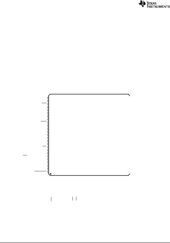
The TMS320F2809, TMS320F2808, TMS320F2806, TMS320F2802, TMS320F2801, TMS320C2802, TMS320C2801, TMS320F28015, and TMS320F28016 100-pin PZ low-profile quad flatpack (LQFP) pin assignments are shown in Figure 2-1, Figure 2-2, Figure 2-3, and Figure 2-4. The 100-ball GGM and ZGM ball grid array (BGA) terminal assignments are shown in Figure 2-5. Table 2-3 describes the function(s) of each pin.
TDO
VSS
XRS
GPIO27/ECAP4/EQEP2S/SPISTEB
EMU0
EMU1
VDDIO
GPIO24/ECAP1/EQEP2A/SPISIMOB
TRST
VDD
X2
VSS
X1
VSS
XCLKIN
GPIO25/ECAP2/EQEP2B/SPISOMIB
GPIO28/SCIRXDA/TZ5
VDD
VSS
GPIO13/TZ2/CANRXB/SPISOMIB
VDD3VFL
TEST1
TEST2
GPIO26/ECAP3/EQEP2I/SPICLKB
GPIO32/SDAA/EPWMSYNCI/ADCSOCAO
|
TCK |
TMS |
|
TDI |
|
GPIO23/EQEP1I/SPISTEC/SCIRXDB |
GPIO22/EQEP1S/SPICLKC/SCITXDB |
GPIO11/EPWM6B/SCIRXDB/ECAP4 |
V |
V |
GPIO21/EQEP1B/SPISOMIC/CANRXB |
XCLKOUT |
V |
|
GPIO10/EPWM6A/CANRXB/ADCSOCBO |
|
GPIO20/EQEP1A/SPISIMOC/CANTXB |
V |
|
GPIO9/EPWM5B/SCITXDB/ECAP3 |
|
GPIO8/EPWM5A/CANTXB/ADCSOCAO |
V |
|
GPIO7/EPWM4B/SPISTED/ECAP2 |
GPIO19/SPISTEA/SCIRXDB |
GPIO6/EPWM4A/EPWMSYNCI/EPWMSYNCO |
|
V |
|
GPIO18/SPICLKA/SCITXDB |
|
GPIO5/EPWM3B/SPICLKD/ECAP1 |
|
GPIO17/SPISOMIA/CANRXB/TZ6 |
|||||||||||||||||||||
|
|
|
|
|
|
|
|
|
|
|
|
|||||||||||||||||||||||||||||||||||||||||||||
|
|
|
|
|
|
|
|
|
|
|
|
|||||||||||||||||||||||||||||||||||||||||||||
|
|
|
|
|
|
|
|
|
|
|
|
|||||||||||||||||||||||||||||||||||||||||||||
|
|
|
|
|
|
|
|
|
|
|
|
|||||||||||||||||||||||||||||||||||||||||||||
|
|
|
|
|
|
|
|
|
|
|
|
|||||||||||||||||||||||||||||||||||||||||||||
|
|
|
|
|
|
|
|
|
|
|
|
|||||||||||||||||||||||||||||||||||||||||||||
|
|
|
|
|
|
|
|
|
|
|
|
|
SS |
DD |
|
|
|
|
DDIO |
|
|
|
|
|
|
SS |
|
|
|
|
|
|
DD |
|
|
|
|
|
|
|
|
SS |
|
|
|
|
|
|
|
|
||||||
|
|
|
|
|
|
|
|
|
|
|
|
|
|
|
|
|
|
|
|
|
|
|
|
|
|
|
|
|
|
|
|
|
|
|
|
|
|
|
|
|
|
|
|
|
|
|
|
|
|
|
|
|
|
|
|
|
|
|
|
|
|
|
|
|
|
|
|
|
|
|
|
|
|
|
|
|
|
|
|
|
|
|
|
|
|
|
|
|
|
|
|
|
|
|
|
|
|
|
|
|
|
|
|
|
|
|
|
|
|
|
|
|
|
75 |
74 |
73 |
72 |
71 |
70 |
69 |
68 |
67 |
66 |
65 |
64 |
63 |
62 |
61 |
60 |
59 |
58 |
57 |
56 |
55 |
54 |
|
53 |
|
52 |
|||||||||||||||||||||||||||||||
76 |
|
|
|
|
|
|
|
|
|
|
|
|
|
|
|
|
|
|
|
|
|
|
|
|
|
|
|
|
|
|
|
|
|
|
|
|
|
|
|
|
|
|
|
|
|
|
|
|
|
|
|
|
|
|
|
|
77 |
|
|
|
|
|
|
|
|
|
|
|
|
|
|
|
|
|
|
|
|
|
|
|
|
|
|
|
|
|
|
|
|
|
|
|
|
|
|
|
|
|
|
|
|
|
|
|
|
|
|
|
|
|
|
|
|
78 |
|
|
|
|
|
|
|
|
|
|
|
|
|
|
|
|
|
|
|
|
|
|
|
|
|
|
|
|
|
|
|
|
|
|
|
|
|
|
|
|
|
|
|
|
|
|
|
|
|
|
|
|
|
|
|
|
79 |
|
|
|
|
|
|
|
|
|
|
|
|
|
|
|
|
|
|
|
|
|
|
|
|
|
|
|
|
|
|
|
|
|
|
|
|
|
|
|
|
|
|
|
|
|
|
|
|
|
|
|
|
|
|
|
|
80 |
|
|
|
|
|
|
|
|
|
|
|
|
|
|
|
|
|
|
|
|
|
|
|
|
|
|
|
|
|
|
|
|
|
|
|
|
|
|
|
|
|
|
|
|
|
|
|
|
|
|
|
|
|
|
|
|
81 |
|
|
|
|
|
|
|
|
|
|
|
|
|
|
|
|
|
|
|
|
|
|
|
|
|
|
|
|
|
|
|
|
|
|
|
|
|
|
|
|
|
|
|
|
|
|
|
|
|
|
|
|
|
|
|
|
82 |
|
|
|
|
|
|
|
|
|
|
|
|
|
|
|
|
|
|
|
|
|
|
|
|
|
|
|
|
|
|
|
|
|
|
|
|
|
|
|
|
|
|
|
|
|
|
|
|
|
|
|
|
|
|
|
|
83 |
|
|
|
|
|
|
|
|
|
|
|
|
|
|
|
|
|
|
|
|
|
|
|
|
|
|
|
|
|
|
|
|
|
|
|
|
|
|
|
|
|
|
|
|
|
|
|
|
|
|
|
|
|
|
|
|
84 |
|
|
|
|
|
|
|
|
|
|
|
|
|
|
|
|
|
|
|
|
|
|
|
|
|
|
|
|
|
|
|
|
|
|
|
|
|
|
|
|
|
|
|
|
|
|
|
|
|
|
|
|
|
|
|
|
85 |
|
|
|
|
|
|
|
|
|
|
|
|
|
|
|
|
|
|
|
|
|
|
|
|
|
|
|
|
|
|
|
|
|
|
|
|
|
|
|
|
|
|
|
|
|
|
|
|
|
|
|
|
|
|
|
|
86 |
|
|
|
|
|
|
|
|
|
|
|
|
|
|
|
|
|
|
|
|
|
|
|
|
|
|
|
|
|
|
|
|
|
|
|
|
|
|
|
|
|
|
|
|
|
|
|
|
|
|
|
|
|
|
|
|
87 |
|
|
|
|
|
|
|
|
|
|
|
|
|
|
|
|
|
|
|
|
|
|
|
|
|
|
|
|
|
|
|
|
|
|
|
|
|
|
|
|
|
|
|
|
|
|
|
|
|
|
|
|
|
|
|
|
88 |
|
|
|
|
|
|
|
|
|
|
|
|
|
|
|
|
|
|
|
|
|
|
|
|
|
|
|
|
|
|
|
|
|
|
|
|
|
|
|
|
|
|
|
|
|
|
|
|
|
|
|
|
|
|
|
|
89 |
|
|
|
|
|
|
|
|
|
|
|
|
|
|
|
|
|
|
|
|
|
|
|
|
|
|
|
|
|
|
|
|
|
|
|
|
|
|
|
|
|
|
|
|
|
|
|
|
|
|
|
|
|
|
|
|
90 |
|
|
|
|
|
|
|
|
|
|
|
|
|
|
|
|
|
|
|
|
|
|
|
|
|
|
|
|
|
|
|
|
|
|
|
|
|
|
|
|
|
|
|
|
|
|
|
|
|
|
|
|
|
|
|
|
91 |
|
|
|
|
|
|
|
|
|
|
|
|
|
|
|
|
|
|
|
|
|
|
|
|
|
|
|
|
|
|
|
|
|
|
|
|
|
|
|
|
|
|
|
|
|
|
|
|
|
|
|
|
|
|
|
|
92 |
|
|
|
|
|
|
|
|
|
|
|
|
|
|
|
|
|
|
|
|
|
|
|
|
|
|
|
|
|
|
|
|
|
|
|
|
|
|
|
|
|
|
|
|
|
|
|
|
|
|
|
|
|
|
|
|
93 |
|
|
|
|
|
|
|
|
|
|
|
|
|
|
|
|
|
|
|
|
|
|
|
|
|
|
|
|
|
|
|
|
|
|
|
|
|
|
|
|
|
|
|
|
|
|
|
|
|
|
|
|
|
|
|
|
94 |
|
|
|
|
|
|
|
|
|
|
|
|
|
|
|
|
|
|
|
|
|
|
|
|
|
|
|
|
|
|
|
|
|
|
|
|
|
|
|
|
|
|
|
|
|
|
|
|
|
|
|
|
|
|
|
|
95 |
|
|
|
|
|
|
|
|
|
|
|
|
|
|
|
|
|
|
|
|
|
|
|
|
|
|
|
|
|
|
|
|
|
|
|
|
|
|
|
|
|
|
|
|
|
|
|
|
|
|
|
|
|
|
|
|
96 |
|
|
|
|
|
|
|
|
|
|
|
|
|
|
|
|
|
|
|
|
|
|
|
|
|
|
|
|
|
|
|
|
|
|
|
|
|
|
|
|
|
|
|
|
|
|
|
|
|
|
|
|
|
|
|
|
97 |
|
|
|
|
|
|
|
|
|
|
|
|
|
|
|
|
|
|
|
|
|
|
|
|
|
|
|
|
|
|
|
|
|
|
|
|
|
|
|
|
|
|
|
|
|
|
|
|
|
|
|
|
|
|
|
|
98 |
|
|
|
|
|
|
|
|
|
|
|
|
|
|
|
|
|
|
|
|
|
|
|
|
|
|
|
|
|
|
|
|
|
|
|
|
|
|
|
|
|
|
|
|
|
|
|
|
|
|
|
|
|
|
|
|
99 |
|
|
|
|
|
|
|
|
|
|
|
|
|
|
|
|
|
|
|
|
|
|
|
|
|
|
|
|
|
|
|
|
|
|
|
|
|
|
|
|
|
|
|
|
|
|
|
|
|
|
|
|
|
|
|
|
100 |
|
|
|
|
|
|
|
|
|
|
|
|
|
|
|
|
|
10 |
|
|
12 |
13 |
14 |
15 |
|
16 |
17 |
|
18 |
19 |
|
20 |
|
21 |
|
22 |
|
23 |
|
24 |
||||||||||||||||
1 |
2 |
3 |
4 |
5 |
6 |
7 |
8 |
9 |
11 |
|
|
|
|
|
|
|
||||||||||||||||||||||||||||||||||||||||
|
|
|
|
|
|
|
|
|
|
|
|
|
|
|
|
|
|
|
|
|
|
|
|
|
||||||||||||||||||||||||||||||||
|
|
|
|
|
|
|
|
|
|
|
|
|
|
|
|
|
|
|
|
|
|
|
|
|
|
|
|
|
|
|
|
|
|
|
|
|
|
|
|
|
|
|
|
|
|
|
|
|
|
|
|
|
|
|
|
|
GPIO12/TZ1/CANTXB/SPISIMOB |
V |
V |
GPIO29/SCITXDA/TZ6 |
GPIO33/SCLA/EPWMSYNCO/ADCSOCBO |
GPIO30/CANRXA |
GPIO31/CANTXA |
GPIO14/TZ3/SCITXDB/SPICLKB |
GPIO15/TZ4/SCIRXDB/SPISTEB |
V |
V |
V |
V |
V |
V |
ADCINA7 |
ADCINA6 |
ADCINA5 |
ADCINA4 |
ADCINA3 |
ADCINA2 |
ADCINA1 |
ADCINA0 |
ADCLO |
|||||||||||||||||||||||||||||||||
|
|
|
SS |
DDIO |
|
|
|
|
|
|
|
|
|
|
|
|
|
DD |
SS |
|
DD1A18 |
|
SS1AGND |
SSA2 |
|
DDA2 |
|
|
|
|
|
|
|
|
|
|
|
|
|
|
|
|
|
|
|
|
|
|
|
|||||||
GPIO4/EPWM3A |
|
|
|
||
|
|
|
|
|
|
51 |
|
|
|
||
|
|
|
|||
|
GPIO16/SPISIMOA/CANTXB/TZ5 |
||||
50 |
|
||||
49 |
|
VSS |
|||
|
|||||
|
|||||
48 |
|
GPIO3/EPWM2B/SPISOMID |
|||
47 |
|
||||
|
GPIO0/EPWM1A |
||||
|
|||||
46 |
|
VDDIO |
|||
|
|||||
|
|||||
45 |
|
GPIO2/EPWM2A |
|||
|
|||||
44 |
|
GPIO1/EPWM1B/SPISIMOD |
|||
|
|||||
|
|||||
43 |
|
GPIO34 |
|||
|
|||||
42 |
|
VDD |
|||
|
|||||
|
|||||
41 |
|
VSS |
|||
|
|
|
|
||
40 |
|
VDD2A18 |
|||
|
|
|
|
||
39 |
|
VSS2AGND |
|||
|
|||||
38 |
|
ADCRESEXT |
|||
|
|||||
37 |
|
ADCREFP |
|||
|
|||||
|
|||||
36 |
|
ADCREFM |
|||
|
|||||
35 |
|
ADCREFIN |
|||
|
|||||
|
|||||
34 |
|
ADCINB7 |
|||
|
|||||
33 |
|
ADCINB6 |
|||
|
|||||
|
|||||
32 |
|
ADCINB5 |
|||
|
|||||
|
|||||
31 |
|
ADCINB4 |
|||
|
|||||
30 |
|
ADCINB3 |
|||
|
|||||
|
|
|
|
||
29 |
|
ADCINB2 |
|||
|
|||||
28 |
|
ADCINB1 |
|||
|
|||||
27 |
|
ADCINB0 |
|||
|
|||||
|
|||||
26 |
|
VDDAIO |
|||
|
|||||
25 |
|
|
|||
|
|
|
|
||
|
|
|
|
|
|
|
|
|
|
|
|
|
SSAIO |
|
|
|
|
V |
|
|
|
||
Figure 2-1. TMS320F2809, TMS320F2808 100-Pin PZ LQFP (Top View)
14 |
Introduction |
Copyright © 2003–2009, Texas Instruments Incorporated |
Submit Documentation Feedback
Product Folder Link(s): TMS320F2809 TMS320F2808 TMS320F2806 TMS320F2802 TMS320F2801 TMS320C2802
TMS320C2801 TMS320F28016 TMS320F28015
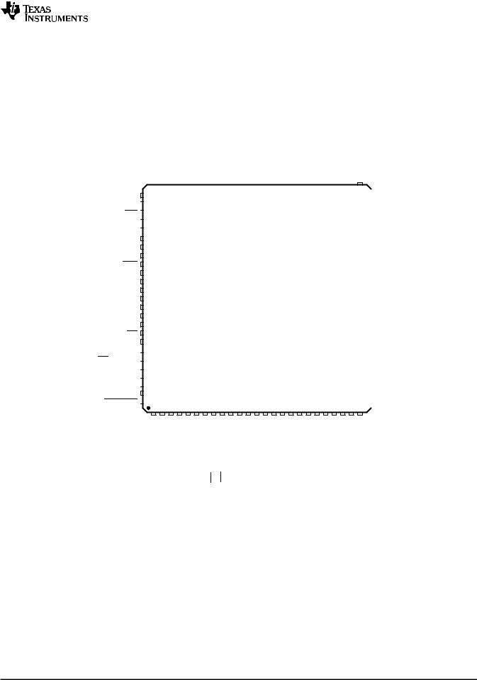
TMS320F2809, TMS320F2808, TMS320F2806
TMS320F2802, TMS320F2801, TMS320C2802
TMS320C2801, TMS320F28016, TMS320F28015
www.ti.com |
SPRS230L –OCTOBER 2003 –REVISED DECEMBER 2009 |
TDO
VSS
XRS
GPIO27/ECAP4/EQEP2S/SPISTEB
EMU0
EMU1
VDDIO
GPIO24/ECAP1/EQEP2A/SPISIMOB
TRST
VDD
X2
VSS
X1
VSS
XCLKIN
GPIO25/ECAP2/EQEP2B/SPISOMIB
GPIO28/SCIRXDA/TZ5
VDD
VSS
GPIO13/TZ2/SPISOMIB
VDD3VFL
TEST1
TEST2
GPIO26/ECAP3/EQEP2I/SPICLKB
GPIO32/SDAA/EPWMSYNCI/ADCSOCAO
TCK |
TMS |
TDI |
GPIO23/EQEP1I/SPISTEC/SCIRXDB |
GPIO22/EQEP1S/SPICLKC/SCITXDB |
GPIO11/EPWM6B/SCIRXDB/ECAP4 |
V |
V |
GPIO21/EQEP1B/SPISOMIC |
XCLKOUT |
V |
|
GPIO10/EPWM6A/ADCSOCBO |
GPIO20/EQEP1A/SPISIMOC |
V |
GPIO9/EPWM5B/SCITXDB/ECAP3 |
|
GPIO8/EPWM5A/ADCSOCAO |
V |
GPIO7/EPWM4B/SPISTED/ECAP2 |
GPIO19/SPISTEA/SCIRXDB |
GPIO6/EPWM4A/EPWMSYNCI/EPWMSYNCO |
V |
GPIO18/SPICLKA/SCITXDB |
GPIO5/EPWM3B/SPICLKD/ECAP1 |
|
GPIO17/SPISOMIA/TZ6 |
|||||||||||||||||||||||
|
|
|
|||||||||||||||||||||||||||||||||||||||||||||||
|
|
|
|||||||||||||||||||||||||||||||||||||||||||||||
|
|
|
|||||||||||||||||||||||||||||||||||||||||||||||
|
|
|
|||||||||||||||||||||||||||||||||||||||||||||||
|
|||||||||||||||||||||||||||||||||||||||||||||||||
|
|
||||||||||||||||||||||||||||||||||||||||||||||||
|
|
|
|
|
|
|
|
|
|
|
|
SS |
DD |
|
|
|
|
DDIO |
|
|
|
|
|
SS |
|
|
|
|
|
DD |
|
|
|
|
|
|
SS |
|
|
|
|
|
|
||||||
|
|
|
|
|
|
|
|
|
|
|
|
|
|
|
|
|
|
|
|
|
|
|
|
|
|
|
|
|
|
|
|
|
|
|
|
|
|
|
|
|
|
|
|
|
|
|
|
|
|
|
|
|
|
|
|
|
|
|
|
|
|
|
|
|
|
|
|
|
|
|
|
|
|
|
|
|
|
|
|
|
|
|
|
|
|
|
|
|
|
|
|
|
|
|
|
|
|
|
|
75 |
74 |
73 |
72 |
71 |
70 |
69 |
68 |
67 |
66 |
65 |
64 |
63 |
62 |
61 |
60 |
59 |
58 |
57 |
56 |
55 |
54 |
|
53 |
|
52 |
||||||||||||||||||||||||
76  77
77  78
78  79
79  80
80
81
82
83
84
85
86
87
88
89
90
91
92
93  94
94  95
95  96
96  97
97  98
98
99
 100
100
1 |
2 |
3 |
4 |
5 |
6 |
7 |
8 |
9 |
10 |
11 |
12 |
13 |
14 |
15 |
16 |
17 |
18 |
19 |
20 |
21 |
22 |
23 |
24 |
GPIO12/TZ1/SPISIMOB |
V |
V |
GPIO29/SCITXDA/TZ6 |
GPIO33/SCLA/EPWMSYNCO/ADCSOCBO |
GPIO30/CANRXA |
GPIO31/CANTXA |
GPIO14/TZ3/SCITXDB/SPICLKB |
GPIO15/TZ4/SCIRXDB/SPISTEB |
V |
V |
V |
V |
V |
V |
ADCINA7 |
ADCINA6 |
ADCINA5 |
ADCINA4 |
ADCINA3 |
ADCINA2 |
ADCINA1 |
ADCINA0 |
ADCLO |
|
SS |
DDIO |
|
|
|
|
|
|
DD |
SS |
DD1A18 |
SS1AGND |
SSA2 |
DDA2 |
|
|
|
|
|
|
|
|
|
51 GPIO4/EPWM3A
VSSAIO 25
|
|
|
|
|
50 |
|
GPIO16/SPISIMOA/TZ5 |
||
49 |
|
VSS |
||
|
||||
|
||||
48 |
|
GPIO3/EPWM2B/SPISOMID |
||
|
||||
47 |
|
GPIO0/EPWM1A |
||
|
||||
|
||||
46 |
|
VDDIO |
||
|
||||
|
||||
45 |
|
GPIO2/EPWM2A |
||
44 |
|
GPIO1/EPWM1B/SPISIMOD |
||
|
||||
|
||||
43 |
|
GPIO34 |
||
|
||||
42 |
|
VDD |
||
|
||||
41 |
|
VSS |
||
|
||||
40 |
|
VDD2A18 |
||
|
||||
39 |
|
VSS2AGND |
||
|
||||
38 |
|
ADCRESEXT |
||
|
||||
|
||||
37 |
|
ADCREFP |
||
|
||||
|
||||
36 |
|
ADCREFM |
||
|
||||
35 |
|
ADCREFIN |
||
|
||||
34 |
|
ADCINB7 |
||
|
||||
33 |
|
ADCINB6 |
||
|
||||
32 |
|
ADCINB5 |
||
|
||||
31 |
|
ADCINB4 |
||
|
||||
30 |
|
ADCINB3 |
||
|
||||
29 |
|
ADCINB2 |
||
|
||||
28 |
|
ADCINB1 |
||
|
||||
27 |
|
ADCINB0 |
||
|
||||
26 |
|
VDDAIO |
||
|
||||
|
|
|||
Figure 2-2. TMS320F2806 100-Pin PZ LQFP (Top View)
Copyright © 2003–2009, Texas Instruments Incorporated |
Introduction |
15 |
Submit Documentation Feedback
Product Folder Link(s): TMS320F2809 TMS320F2808 TMS320F2806 TMS320F2802 TMS320F2801 TMS320C2802
TMS320C2801 TMS320F28016 TMS320F28015
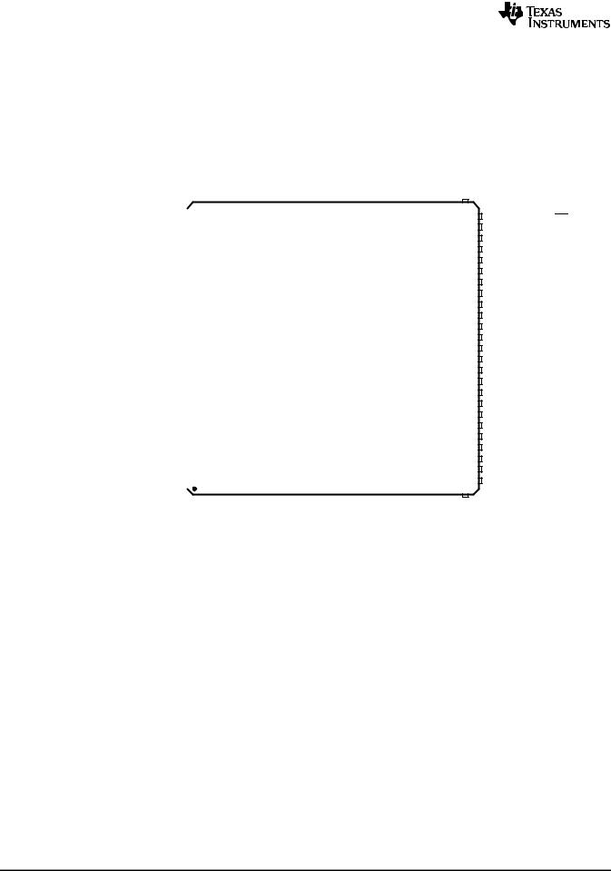
TMS320F2809, TMS320F2808, TMS320F2806
TMS320F2802, TMS320F2801, TMS320C2802
TMS320C2801, TMS320F28016, TMS320F28015
SPRS230L –OCTOBER 2003 –REVISED DECEMBER 2009 |
www.ti.com |
|
|
|
|
|
|
|
|
TCK |
TMS |
TDI |
GPIO23/EQEP1I |
GPIO22/EQEP1S |
GPIO11 |
V |
V |
GPIO21/EQEP1B |
|
XCLKOUT |
|
GPIO10/ADCSOCBO |
GPIO20/EQEP1A |
V |
|
GPIO8/ADCSOCAO |
V |
GPIO7/ECAP2 |
GPIO19/SPISTEA |
GPIO6/EPWMSYNCI/EPWMSYNCO |
V |
GPIO18/SPICLKA |
GPIO5/EPWM3B/ECAP1 |
|
GPIO17/SPISOMIA/TZ6 |
||||||||||||||||||||||||||
|
|
|
|
|
|
|
|
|
|
|
|
|
|
||||||||||||||||||||||||||||||||||||||||||||||
|
|
|
|
|
|
|
|
|
|
|
|||||||||||||||||||||||||||||||||||||||||||||||||
|
|
|
|
|
|
|
|
|
|
|
|
|
|
||||||||||||||||||||||||||||||||||||||||||||||
|
|
|
|
|
|
|
|
|
V |
|
|||||||||||||||||||||||||||||||||||||||||||||||||
|
|
|
|
|
|
|
|
|
GPIO9 |
||||||||||||||||||||||||||||||||||||||||||||||||||
|
|
|
|
|
|
|
|
|
|
|
|
|
|
|
|
|
|
|
|
SS |
|
DD |
|
|
|
|
|
DDIO |
|
|
|
|
SS |
|
|
|
|
|
DD |
|
|
|
|
|
|
SS |
|
|
|
|
|
|
|
||||||
|
|
|
|
|
|
|
|
|
|
|
|
|
|
|
|
|
|
|
|
|
|
|
|
|
|
|
|
|
|
|
|
|
|
|
|
|
|
|
|
|
|
|
|
|
|
|
|
|
|
|
|
|
|
|
|
|
|
|
|
|
|
TDO |
|
75 |
74 |
73 |
72 |
71 |
70 |
69 |
68 |
67 |
66 |
65 |
64 |
63 |
62 |
61 |
60 |
59 |
58 |
57 |
56 |
55 |
54 |
53 |
52 |
||||||||||||||||||||||||||||||||
|
|
|
|||||||||||||||||||||||||||||||||||||||||||||||||||||||||
|
|
|
76 |
|
|
|
|
|
|
|
|
|
|
|
|
|
|
|
|
|
|
|
|
|
|
|
|
|
|
|
|
|
|
|
|
|
|
|
|
|
|
|
|
|
|
|
|
|
|
|
|
|
|
|
|
||||
|
|
|
VSS |
|
|
77 |
|
|
|
|
|
|
|
|
|
|
|
|
|
|
|
|
|
|
|
|
|
|
|
|
|
|
|
|
|
|
|
|
|
|
|
|
|
|
|
|
|
|
|
|
|
|
|
|
|
|
|
|
|
|
|
|
|
|
|
|
|
|
|
|
|
|
|
|
|
|
|
|
|
|
|
|
|
|
|
|
|
|
|
|
|
|
|
|
|
|
|
|
|
|
|
|
|
|
|
|
|
|
|
|
|
|
|
|
|
||||
|
|
|
|
|
|
|
|
|
|
|
|
|
|
|
|
|
|
|
|
|
|
|
|
|
|
|
|
|
|
|
|
|
|
|
|
|
|
|
|
|
|
|
|
|
|
|
|
|
|
|
|
|
|
||||||
|
|
XRS |
|
78 |
|
|
|
|
|
|
|
|
|
|
|
|
|
|
|
|
|
|
|
|
|
|
|
|
|
|
|
|
|
|
|
|
|
|
|
|
|
|
|
|
|
|
|
|
|
|
|
|
|
|
|
|
|||
|
|
|
|
|
|
|
|
|
|
|
|
|
|
|
|
|
|
|
|
|
|
|
|
|
|
|
|
|
|
|
|
|
|
|
|
|
|
|
|
|
|
|
|
|
|
|
|
|
|
|
|
|
|||||||
SPISTEB/GPIO27 |
|
79 |
|
|
|
|
|
|
|
|
|
|
|
|
|
|
|
|
|
|
|
|
|
|
|
|
|
|
|
|
|
|
|
|
|
|
|
|
|
|
|
|
|
|
|
|
|
|
|
|
|
|
|
|
|||||
|
|
|
|
|
|
|
|
|
|
|
|
|
|
|
|
|
|
|
|
|
|
|
|
|
|
|
|
|
|
|
|
|
|
|
|
|
|
|
|
|
|
|
|
|
|
|
|
|
|
|
|
|
|||||||
|
EMU0 |
|
80 |
|
|
|
|
|
|
|
|
|
|
|
|
|
|
|
|
|
|
|
|
|
|
|
|
|
|
|
|
|
|
|
|
|
|
|
|
|
|
|
|
|
|
|
|
|
|
|
|
|
|
|
|
||||
|
|
|
|
|
|
|
|
|
|
|
|
|
|
|
|
|
|
|
|
|
|
|
|
|
|
|
|
|
|
|
|
|
|
|
|
|
|
|
|
|
|
|
|
|
|
|
|
|
|
|
|
|
|
||||||
|
EMU1 |
|
81 |
|
|
|
|
|
|
|
|
|
|
|
|
|
|
|
|
|
|
|
|
|
|
|
|
|
|
|
|
|
|
|
|
|
|
|
|
|
|
|
|
|
|
|
|
|
|
|
|
|
|
|
|
||||
|
|
|
|
|
|
|
|
|
|
|
|
|
|
|
|
|
|
|
|
|
|
|
|
|
|
|
|
|
|
|
|
|
|
|
|
|
|
|
|
|
|
|
|
|
|
|
|
|
|
|
|
|
|
||||||
|
VDDIO |
|
82 |
|
|
|
|
|
|
|
|
|
|
|
|
|
|
|
|
|
|
|
|
|
|
|
|
|
|
|
|
|
|
|
|
|
|
|
|
|
|
|
|
|
|
|
|
|
|
|
|
|
|
|
|
||||
|
|
|
|
|
|
|
|
|
|
|
|
|
|
|
|
|
|
|
|
|
|
|
|
|
|
|
|
|
|
|
|
|
|
|
|
|
|
|
|
|
|
|
|
|
|
|
|
|
|
|
|
|
|
||||||
|
|
|
|
|
|
|
|
|
|
|
|
|
|
|
|
|
|
|
|
|
|
|
|
|
|
|
|
|
|
|
|
|
|
|
|
|
|
|
|
|
|
|
|
|
|
|
|
|
|
|
|
|
|
|
|||||
SPISIMOB/GPIO24/ECAP1 |
|
83 |
|
|
|
|
|
|
|
|
|
|
|
|
|
|
|
|
|
|
|
|
|
|
|
|
|
|
|
|
|
|
|
|
|
|
|
|
|
|
|
|
|
|
|
|
|
|
|
|
|
|
|
|
|||||
|
|
|
|
|
|
|
|
|
|
|
|
|
|
|
|
|
|
|
|
|
|
|
|
|
|
|
|
|
|
|
|
|
|
|
|
|
|
|
|
|
|
|
|
|
|
|
|
|
|
|
|
|
|
|
|
|
|
|
|
|
|
TRST |
|
84 |
|
|
|
|
|
|
|
|
|
|
|
|
|
|
|
|
|
|
|
|
|
|
|
|
|
|
|
|
|
|
|
|
|
|
|
|
|
|
|
|
|
|
|
|
|
|
|
|
|
|
|
|
|||
|
|
|
VDD |
|
85 |
|
|
|
|
|
|
|
|
|
|
|
|
|
|
|
|
|
|
|
|
|
|
|
|
|
|
|
|
|
|
|
|
|
|
|
|
|
|
|
|
|
|
|
|
|
|
|
|
|
|
|
|
||
|
|
|
|
|
|
|
|
|
|
|
|
|
|
|
|
|
|
|
|
|
|
|
|
|
|
|
|
|
|
|
|
|
|
|
|
|
|
|
|
|
|
|
|
|
|
|
|
|
|
|
|
|
|||||||
|
|
|
|
X2 |
|
86 |
|
|
|
|
|
|
|
|
|
|
|
|
|
|
|
|
|
|
|
|
|
|
|
|
|
|
|
|
|
|
|
|
|
|
|
|
|
|
|
|
|
|
|
|
|
|
|
|
|
|
|
|
|
|
|
|
|
|
|
|
|
|
|
|
|
|
|
|
|
|
|
|
|
|
|
|
|
|
|
|
|
|
|
|
|
|
|
|
|
|
|
|
|
|
|
|
|
|
|
|
|
|
|
|
|
|
|
|
|
|
|||
|
|
|
|
VSS |
|
87 |
|
|
|
|
|
|
|
|
|
|
|
|
|
|
|
|
|
|
|
|
|
|
|
|
|
|
|
|
|
|
|
|
|
|
|
|
|
|
|
|
|
|
|
|
|
|
|
|
|
|
|
|
|
|
|
|
|
|
|
|
|
|
|
|
|
|
|
|
|
|
|
|
|
|
|
|
|
|
|
|
|
|
|
|
|
|
|
|
|
|
|
|
|
|
|
|
|
|
|
|
|
|
|
|
|
|
|||||||
|
|
|
|
X1 |
|
88 |
|
|
|
|
|
|
|
|
|
|
|
|
|
|
|
|
|
|
|
|
|
|
|
|
|
|
|
|
|
|
|
|
|
|
|
|
|
|
|
|
|
|
|
|
|
|
|
|
|
|
|
|
|
|
|
|
|
|
|
|
|
|
|
|
|
|
|
|
|
|
|
|
|
|
|
|
|
|
|
|
|
|
|
|
|
|
|
|
|
|
|
|
|
|
|
|
|
|
|
|
|
|
|
|
|
|
|||||||
|
|
|
VSS |
|
89 |
|
|
|
|
|
|
|
|
|
|
|
|
|
|
|
|
|
|
|
|
|
|
|
|
|
|
|
|
|
|
|
|
|
|
|
|
|
|
|
|
|
|
|
|
|
|
|
|
|
|
|
|
||
|
|
|
|
|
|
|
|
|
|
|
|
|
|
|
|
|
|
|
|
|
|
|
|
|
|
|
|
|
|
|
|
|
|
|
|
|
|
|
|
|
|
|
|
|
|
|
|
|
|
|
|
|
|
|
|
||||
|
XCLKIN |
|
90 |
|
|
|
|
|
|
|
|
|
|
|
|
|
|
|
|
|
|
|
|
|
|
|
|
|
|
|
|
|
|
|
|
|
|
|
|
|
|
|
|
|
|
|
|
|
|
|
|
|
|
|
|
||||
|
|
|
|
|
|
|
|
|
|
|
|
|
|
|
|
|
|
|
|
|
|
|
|
|
|
|
|
|
|
|
|
|
|
|
|
|
|
|
|
|
|
|
|
|
|
|
|
|
|
|
|
|
|
||||||
GPIO25/ECAP2/SPISOMIB |
|
91 |
|
|
|
|
|
|
|
|
|
|
|
|
|
|
|
|
|
|
|
|
|
|
|
|
|
|
|
|
|
|
|
|
|
|
|
|
|
|
|
|
|
|
|
|
|
|
|
|
|
|
|
|
|||||
|
|
|
|
|
|
|
|
|
|
|
|
|
|
|
|
|
|
|
|
|
|
|
|
|
|
|
|
|
|
|
|
|
|
|
|
|
|
|
|
|
|
|
|
|
|
|
|
|
|
|
|
|
|||||||
|
|
|
|
|
|
|
|
|
|
|
|
|
|
|
|
|
|
|
|
|
|
|
|
|
|
|
|
|
|
|
|
|
|
|
|
|
|
|
|
|
|
|
|
|
|
|
|
|
|
|
|
|
|
|
|
|
|
|
|
GPIO28/SCIRXDA/TZ5 |
|
92 |
|
|
|
|
|
|
|
|
|
|
|
|
|
|
|
|
|
|
|
|
|
|
|
|
|
|
|
|
|
|
|
|
|
|
|
|
|
|
|
|
|
|
|
|
|
|
|
|
|
|
|
|
|||||
|
|
|
VDD |
|
|
|
|
|
|
|
|
|
|
|
|
|
|
|
|
|
|
|
|
|
|
|
|
|
|
|
|
|
|
|
|
|
|
|
|
|
|
|
|
|
|
|
|
|
|
|
|
|
|
|
|
|
|||
|
|
|
|
93 |
|
|
|
|
|
|
|
|
|
|
|
|
|
|
|
|
|
|
|
|
|
|
|
|
|
|
|
|
|
|
|
|
|
|
|
|
|
|
|
|
|
|
|
|
|
|
|
|
|
|
|
|
|||
|
|
|
|
|
|
|
|
|
|
|
|
|
|
|
|
|
|
|
|
|
|
|
|
|
|
|
|
|
|
|
|
|
|
|
|
|
|
|
|
|
|
|
|
|
|
|
|
|
|
|
|
|
|||||||
|
|
|
VSS |
|
94 |
|
|
|
|
|
|
|
|
|
|
|
|
|
|
|
|
|
|
|
|
|
|
|
|
|
|
|
|
|
|
|
|
|
|
|
|
|
|
|
|
|
|
|
|
|
|
|
|
|
|
|
|
||
|
|
|
|
|
|
|
|
|
|
|
|
|
|
|
|
|
|
|
|
|
|
|
|
|
|
|
|
|
|
|
|
|
|
|
|
|
|
|
|
|
|
|
|
|
|
|
|
|
|
|
|
|
|||||||
|
|
|
|
|
|
|
95 |
|
|
|
|
|
|
|
|
|
|
|
|
|
|
|
|
|
|
|
|
|
|
|
|
|
|
|
|
|
|
|
|
|
|
|
|
|
|
|
|
|
|
|
|
|
|
|
|
|
|
|
|
SPISOMIB/GPIO13/TZ2 |
|
|
|
|
|
|
|
|
|
|
|
|
|
|
|
|
|
|
|
|
|
|
|
|
|
|
|
|
|
|
|
|
|
|
|
|
|
|
|
|
|
|
|
|
|
|
|
|
|
|
|
|
|
|
|||||
|
|
|
|
|
|
|
|
|
|
|
|
|
|
|
|
|
|
|
|
|
|
|
|
|
|
|
|
|
|
|
|
|
|
|
|
|
|
|
|
|
|
|
|
|
|
|
|
|
|
|
|
|
|
||||||
VDD3VFL(A) |
|
96 |
|
|
|
|
|
|
|
|
|
|
|
|
|
|
|
|
|
|
|
|
|
|
|
|
|
|
|
|
|
|
|
|
|
|
|
|
|
|
|
|
|
|
|
|
|
|
|
|
|
|
|
|
|||||
|
|
|
|
|
|
|
|
|
|
|
|
|
|
|
|
|
|
|
|
|
|
|
|
|
|
|
|
|
|
|
|
|
|
|
|
|
|
|
|
|
|
|
|
|
|
|
|
|
|
|
|
|
|||||||
|
97 |
|
|
|
|
|
|
|
|
|
|
|
|
|
|
|
|
|
|
|
|
|
|
|
|
|
|
|
|
|
|
|
|
|
|
|
|
|
|
|
|
|
|
|
|
|
|
|
|
|
|
|
|
||||||
|
TEST1 |
|
98 |
|
|
|
|
|
|
|
|
|
|
|
|
|
|
|
|
|
|
|
|
|
|
|
|
|
|
|
|
|
|
|
|
|
|
|
|
|
|
|
|
|
|
|
|
|
|
|
|
|
|
|
|
||||
|
TEST2 |
|
|
|
|
|
|
|
|
|
|
|
|
|
|
|
|
|
|
|
|
|
|
|
|
|
|
|
|
|
|
|
|
|
|
|
|
|
|
|
|
|
|
|
|
|
|
|
|
|
|
|
|
|
|||||
SPICLKB/GPIO26 |
|
99 |
|
|
|
|
|
|
|
|
|
|
|
|
|
|
|
|
|
|
|
|
|
|
|
|
|
|
|
|
|
|
|
|
|
|
|
|
|
|
|
|
|
|
|
|
|
|
|
|
|
|
|
|
|||||
|
|
|
|
|
|
|
|
|
|
|
|
|
|
|
|
|
|
|
|
|
|
|
|
|
|
|
|
|
|
|
|
|
|
|
|
|
|
|
|
|
|
|
|
|
|
|
|
|
|
|
|
|
|
|
|
|
|
||
GPIO32/SDAA/EPWMSYNCI/ADSOCAO |
|
100 |
|
|
|
|
|
|
|
|
|
|
|
|
|
|
|
|
|
|
|
|
|
|
|
|
|
|
|
|
|
|
|
|
|
|
|
|
|
|
|
|
|
|
|
|
|
|
|
|
|
|
|
||||||
|
|
|
|
|
|
|
1 |
2 |
3 |
4 |
5 |
6 |
7 |
8 |
9 |
10 |
11 |
12 |
13 |
14 |
15 |
16 |
|
17 |
18 |
|
19 |
|
20 |
|
21 |
|
22 |
|
23 |
|
24 |
||||||||||||||||||||||
|
|
|
|
|
|
|
|
|
|
|
|
|
|
|
|
|
|
|
|
|
|
|
|
|
|
|
|
|
|
|
|
|
|
||||||||||||||||||||||||||
|
|
|
|
|
|
|
|
|
|
|
|
|
|
|
|
|
|
|
|
|
|
|
|
|
|
|
|
|
|
|
|
|
|
|
|
||||||||||||||||||||||||
|
|
|
|
|
|
|
|
|
|
|
|
|
|
|
|
|
|
|
|
|
|
|
|
|
|
|
|
|
|
|
|
|
|
|
|
|
|
|
|
|
|
|
|
|
|
|
|
|
|
|
|
|
|
|
|
|
|
|
|
|
|
|
|
|
|
|
|
SPISIMOB/GPIO12/TZ1 |
V |
V |
GPIO29/SCITXDA/TZ6 |
GPIO33/SCLA/EPWMSYNCO/ADCSOCBO |
GPIO30/CANRXA |
GPIO31/CANTXA |
|
SPICLKB/GPIO14/TZ3 |
SPISTEB/GPIO15/TZ4 |
V |
V |
V |
V |
V |
V |
ADCINA7 |
|
ADCINA6 |
ADCINA5 |
ADCINA4 |
ADCINA3 |
ADCINA2 |
ADCINA1 |
|
ADCINA0 |
|
ADCLO |
||||||||||||||||||||||||
|
|
|
|
|
|
|
|
|
|
SS |
DDIO |
|
|
|
|
|
|
|
|
|
|
|
|
|
|
DD |
SS |
DD1A18 |
SS1AGND |
SSA2 |
DDA2 |
|
|
|
|
|
|
|
|
|
|
|
|
|
|
|
|
|
|
|
|
||||||||
|
|
|
|
|
|
|
|
|
|
|
|
|
|
|
|
|
|
|
|
|
|
|
|
|
|
|
|
|
|
|
|
|
|
|
|
|
|
|
|
|
|
|
|
|
|
|
|
|
|
||||||||||
|
|
|
|
|
|
|
|
|
|
|
|
|
|
|
|
|
|
|
|
|
|
|
|
|
|
|
|
|
|
|
|
|
|
|
|
|
|
|
|
|
|
|
|
|
|
|
|
|
|
|
|
|
|
|
|
|
|
|
|
A.On the C280x devices, the VDD3VFL pin is VDDIO.
GPIO4/EPWM3A
51 50
49
48
47
46
45
44
43
42
41
40
39
38
37
36
35
34
33
32
31
30
29
28
27
26 25
SSAIO
V
GPIO16/SPISIMOA/TZ5
VSS
GPIO3/EPWM2B
GPIO0/EPWM1A
VDDIO
GPIO2/EPWM2A
GPIO1/EPWM1B
GPIO34
VDD
VSS
VDD2A18
VSS2AGND
ADCRESEXT
ADCREFP
ADCREFM
ADCREFIN
ADCINB7
ADCINB6
ADCINB5
ADCINB4
ADCINB3
ADCINB2
ADCINB1
ADCINB0
VDDAIO
Figure 2-3. TMS320F2802, TMS320F2801, TMS320C2802, TMS320C2801 100-Pin PZ LQFP (Top View)
16 |
Introduction |
Copyright © 2003–2009, Texas Instruments Incorporated |
Submit Documentation Feedback
Product Folder Link(s): TMS320F2809 TMS320F2808 TMS320F2806 TMS320F2802 TMS320F2801 TMS320C2802
TMS320C2801 TMS320F28016 TMS320F28015
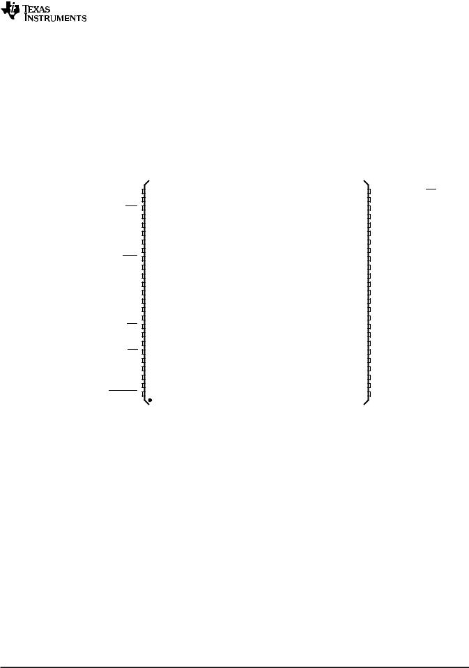
TMS320F2809, TMS320F2808, TMS320F2806
TMS320F2802, TMS320F2801, TMS320C2802
TMS320C2801, TMS320F28016, TMS320F28015
www.ti.com |
SPRS230L –OCTOBER 2003 –REVISED DECEMBER 2009 |
TDO
VSS
XRS
GPIO27
EMU0
EMU1
VDDIO
GPIO24/ECAP1
TRST
VDD
X2
VSS
X1
VSS
XCLKIN
GPIO25/ECAP2
GPIO28/SCIRXDA/TZ5
VDD
VSS
GPIO13/TZ2
VDD3VFL(A)
TEST1
TEST2
GPIO26
GPIO32/SDAA/EPWMSYNCI/ADSOCAO
|
|
|
TCK |
|
TMS |
|
TDI |
GPIO23 |
|
GPIO22 |
GPIO11 |
|
|
|
GPIO21 |
|
XCLKOUT |
|
GPIO10/ADCSOCBO |
|
GPIO20 |
|
|
GPIO8/ADCSOCAO |
|
|
GPIO7/EPWM4B/ECAP2 |
|
GPIO19/SPISTEA |
|
GPIO6/EPWM4A/EPWMSYNCI/EPWMSYNCO |
|
V |
GPIO18/SPICLKA |
GPIO5/EPWM3B/ECAP1 |
|
GPIO17/SPISOMIA/TZ6 |
GPIO4/EPWM3A |
||||||||||||||||||||||||||||||||||||||||||||||||||||||||||||||||||||||
|
|
|
|
|
|
|
|
|
|
|
|
|
|
|
|
|
|
|
|
|
|
|
|
|
|
|
|
|
|
|
|
|
|
|
|
|
|
|
|
|||||||||||||||||||||||||||||||||||||||||||||||||||||||||||||||||||||
|
|
|
|
|
|
|
|
|
|
|
|
|
|
|
|
|
|
|
||||||||||||||||||||||||||||||||||||||||||||||||||||||||||||||||||||||||||||||||||||||||||
|
|
|
|
|
|
|
|
|
|
|
|
|
|
|
|
|
|
|
|
|
|
|
|
|
|
|
|
|
|
|
|
|
|
|
|
|
|
|
|
|||||||||||||||||||||||||||||||||||||||||||||||||||||||||||||||||||||
|
|
|
|
|
|
V |
V |
|
|
V |
|
V |
|
V |
|
|
|
|
||||||||||||||||||||||||||||||||||||||||||||||||||||||||||||||||||||||||||||||||||||||||||
|
|
|
|
|
|
|
|
|
GPIO9 |
|
|
|
|
|||||||||||||||||||||||||||||||||||||||||||||||||||||||||||||||||||||||||||||||||||||||||||||||
|
|
|
|
|
|
|
|
|
|
|
|
|
|
|
|
|
|
|
|
|
|
|
|
|
|
|
SS |
|
|
DD |
|
|
|
|
|
|
|
|
|
|
|
DDIO |
|
|
|
|
|
|
|
|
|
SS |
|
|
|
|
|
|
|
|
|
|
DD |
|
|
|
|
|
|
|
|
|
|
|
|
|
SS |
|
|
|
|
|
|
|
|
|
|
|
|
|
|
|
|
|
|
|
||||||||||||
|
|
|
|
|
|
|
|
|
|
|
|
|
|
|
|
|
|
|
|
|
|
|
|
|
|
|
|
|
|
|
|
|
|
|
|
|
|
|
|
|
|
|
|
|
|
|
|
|
|
|
|
|
|
|
|
|
|
|
|
|
|
|
|
|
|
|
|
|
|
|
|
|
|
|
|
|
|
|
|
|
|
|
|
|
|
|
|
|
|
|
|
|
|
|
|
|
|
|
|
|
|
|
|
|
|
|
|
|
75 |
74 |
73 |
72 |
71 |
70 |
69 |
68 |
67 |
66 |
65 |
64 |
63 |
62 |
61 |
60 |
59 |
58 |
57 |
56 |
55 |
54 |
53 |
52 |
51 |
|
|
||||||||||||||||||||||||||||||||||||||||||||||||||||||||||||||||||||||||||||||||||
76 |
|
|
|
|
|
|
|
|
|
|
|
|
|
|
|
|
|
|
|
|
|
|
|
|
|
|
|
|
|
|
|
|
|
|
|
|
|
|
|
|
|
|
|
|
|
|
|
|
|
|
|
|
|
|
|
|
|
|
|
|
|
|
|
|
|
|
|
|
|
|
|
|
|
|
|
|
|
|
|
|
|
|
|
|
|
|
|
|
|
|
|
|
|
|
|
|
|
|
|
|
|
50 |
||||||
77 |
|
|
|
|
|
|
|
|
|
|
|
|
|
|
|
|
|
|
|
|
|
|
|
|
|
|
|
|
|
|
|
|
|
|
|
|
|
|
|
|
|
|
|
|
|
|
|
|
|
|
|
|
|
|
|
|
|
|
|
|
|
|
|
|
|
|
|
|
|
|
|
|
|
|
|
|
|
|
|
|
|
|
|
|
|
|
|
|
|
|
|
|
|
|
|
|
|
|
|
|
|
49 |
||||||
78 |
|
|
|
|
|
|
|
|
|
|
|
|
|
|
|
|
|
|
|
|
|
|
|
|
|
|
|
|
|
|
|
|
|
|
|
|
|
|
|
|
|
|
|
|
|
|
|
|
|
|
|
|
|
|
|
|
|
|
|
|
|
|
|
|
|
|
|
|
|
|
|
|
|
|
|
|
|
|
|
|
|
|
|
|
|
|
|
|
|
|
|
|
|
|
|
|
|
|
|
|
|
48 |
||||||
79 |
|
|
|
|
|
|
|
|
|
|
|
|
|
|
|
|
|
|
|
|
|
|
|
|
|
|
|
|
|
|
|
|
|
|
|
|
|
|
|
|
|
|
|
|
|
|
|
|
|
|
|
|
|
|
|
|
|
|
|
|
|
|
|
|
|
|
|
|
|
|
|
|
|
|
|
|
|
|
|
|
|
|
|
|
|
|
|
|
|
|
|
|
|
|
|
|
|
|
|
|
|
47 |
||||||
80 |
|
|
|
|
|
|
|
|
|
|
|
|
|
|
|
|
|
|
|
|
|
|
|
|
|
|
|
|
|
|
|
|
|
|
|
|
|
|
|
|
|
|
|
|
|
|
|
|
|
|
|
|
|
|
|
|
|
|
|
|
|
|
|
|
|
|
|
|
|
|
|
|
|
|
|
|
|
|
|
|
|
|
|
|
|
|
|
|
|
|
|
|
|
|
|
|
|
|
|
|
|
46 |
||||||
81 |
|
|
|
|
|
|
|
|
|
|
|
|
|
|
|
|
|
|
|
|
|
|
|
|
|
|
|
|
|
|
|
|
|
|
|
|
|
|
|
|
|
|
|
|
|
|
|
|
|
|
|
|
|
|
|
|
|
|
|
|
|
|
|
|
|
|
|
|
|
|
|
|
|
|
|
|
|
|
|
|
|
|
|
|
|
|
|
|
|
|
|
|
|
|
|
|
|
|
|
|
|
45 |
||||||
82 |
|
|
|
|
|
|
|
|
|
|
|
|
|
|
|
|
|
|
|
|
|
|
|
|
|
|
|
|
|
|
|
|
|
|
|
|
|
|
|
|
|
|
|
|
|
|
|
|
|
|
|
|
|
|
|
|
|
|
|
|
|
|
|
|
|
|
|
|
|
|
|
|
|
|
|
|
|
|
|
|
|
|
|
|
|
|
|
|
|
|
|
|
|
|
|
|
|
|
|
|
|
44 |
||||||
83 |
|
|
|
|
|
|
|
|
|
|
|
|
|
|
|
|
|
|
|
|
|
|
|
|
|
|
|
|
|
|
|
|
|
|
|
|
|
|
|
|
|
|
|
|
|
|
|
|
|
|
|
|
|
|
|
|
|
|
|
|
|
|
|
|
|
|
|
|
|
|
|
|
|
|
|
|
|
|
|
|
|
|
|
|
|
|
|
|
|
|
|
|
|
|
|
|
|
|
|
|
|
43 |
||||||
84 |
|
|
|
|
|
|
|
|
|
|
|
|
|
|
|
|
|
|
|
|
|
|
|
|
|
|
|
|
|
|
|
|
|
|
|
|
|
|
|
|
|
|
|
|
|
|
|
|
|
|
|
|
|
|
|
|
|
|
|
|
|
|
|
|
|
|
|
|
|
|
|
|
|
|
|
|
|
|
|
|
|
|
|
|
|
|
|
|
|
|
|
|
|
|
|
|
|
|
|
|
|
42 |
||||||
85 |
|
|
|
|
|
|
|
|
|
|
|
|
|
|
|
|
|
|
|
|
|
|
|
|
|
|
|
|
|
|
|
|
|
|
|
|
|
|
|
|
|
|
|
|
|
|
|
|
|
|
|
|
|
|
|
|
|
|
|
|
|
|
|
|
|
|
|
|
|
|
|
|
|
|
|
|
|
|
|
|
|
|
|
|
|
|
|
|
|
|
|
|
|
|
|
|
|
|
|
|
|
41 |
||||||
86 |
|
|
|
|
|
|
|
|
|
|
|
|
|
|
|
|
|
|
|
|
|
|
|
|
|
|
|
|
|
|
|
|
|
|
|
|
|
|
|
|
|
|
|
|
|
|
|
|
|
|
|
|
|
|
|
|
|
|
|
|
|
|
|
|
|
|
|
|
|
|
|
|
|
|
|
|
|
|
|
|
|
|
|
|
|
|
|
|
|
|
|
|
|
|
|
|
|
|
|
|
|
40 |
||||||
87 |
|
|
|
|
|
|
|
|
|
|
|
|
|
|
|
|
|
|
|
|
|
|
|
|
|
|
|
|
|
|
|
|
|
|
|
|
|
|
|
|
|
|
|
|
|
|
|
|
|
|
|
|
|
|
|
|
|
|
|
|
|
|
|
|
|
|
|
|
|
|
|
|
|
|
|
|
|
|
|
|
|
|
|
|
|
|
|
|
|
|
|
|
|
|
|
|
|
|
|
|
|
39 |
||||||
88 |
|
|
|
|
|
|
|
|
|
|
|
|
|
|
|
|
|
|
|
|
|
|
|
|
|
|
|
|
|
|
|
|
|
|
|
|
|
|
|
|
|
|
|
|
|
|
|
|
|
|
|
|
|
|
|
|
|
|
|
|
|
|
|
|
|
|
|
|
|
|
|
|
|
|
|
|
|
|
|
|
|
|
|
|
|
|
|
|
|
|
|
|
|
|
|
|
|
|
|
|
|
38 |
||||||
89 |
|
|
|
|
|
|
|
|
|
|
|
|
|
|
|
|
|
|
|
|
|
|
|
|
|
|
|
|
|
|
|
|
|
|
|
|
|
|
|
|
|
|
|
|
|
|
|
|
|
|
|
|
|
|
|
|
|
|
|
|
|
|
|
|
|
|
|
|
|
|
|
|
|
|
|
|
|
|
|
|
|
|
|
|
|
|
|
|
|
|
|
|
|
|
|
|
|
|
|
|
|
37 |
||||||
90 |
|
|
|
|
|
|
|
|
|
|
|
|
|
|
|
|
|
|
|
|
|
|
|
|
|
|
|
|
|
|
|
|
|
|
|
|
|
|
|
|
|
|
|
|
|
|
|
|
|
|
|
|
|
|
|
|
|
|
|
|
|
|
|
|
|
|
|
|
|
|
|
|
|
|
|
|
|
|
|
|
|
|
|
|
|
|
|
|
|
|
|
|
|
|
|
|
|
|
|
|
|
36 |
||||||
91 |
|
|
|
|
|
|
|
|
|
|
|
|
|
|
|
|
|
|
|
|
|
|
|
|
|
|
|
|
|
|
|
|
|
|
|
|
|
|
|
|
|
|
|
|
|
|
|
|
|
|
|
|
|
|
|
|
|
|
|
|
|
|
|
|
|
|
|
|
|
|
|
|
|
|
|
|
|
|
|
|
|
|
|
|
|
|
|
|
|
|
|
|
|
|
|
|
|
|
|
|
|
35 |
||||||
92 |
|
|
|
|
|
|
|
|
|
|
|
|
|
|
|
|
|
|
|
|
|
|
|
|
|
|
|
|
|
|
|
|
|
|
|
|
|
|
|
|
|
|
|
|
|
|
|
|
|
|
|
|
|
|
|
|
|
|
|
|
|
|
|
|
|
|
|
|
|
|
|
|
|
|
|
|
|
|
|
|
|
|
|
|
|
|
|
|
|
|
|
|
|
|
|
|
|
|
|
|
|
34 |
||||||
93 |
|
|
|
|
|
|
|
|
|
|
|
|
|
|
|
|
|
|
|
|
|
|
|
|
|
|
|
|
|
|
|
|
|
|
|
|
|
|
|
|
|
|
|
|
|
|
|
|
|
|
|
|
|
|
|
|
|
|
|
|
|
|
|
|
|
|
|
|
|
|
|
|
|
|
|
|
|
|
|
|
|
|
|
|
|
|
|
|
|
|
|
|
|
|
|
|
|
|
|
|
|
33 |
||||||
94 |
|
|
|
|
|
|
|
|
|
|
|
|
|
|
|
|
|
|
|
|
|
|
|
|
|
|
|
|
|
|
|
|
|
|
|
|
|
|
|
|
|
|
|
|
|
|
|
|
|
|
|
|
|
|
|
|
|
|
|
|
|
|
|
|
|
|
|
|
|
|
|
|
|
|
|
|
|
|
|
|
|
|
|
|
|
|
|
|
|
|
|
|
|
|
|
|
|
|
|
|
|
32 |
||||||
95 |
|
|
|
|
|
|
|
|
|
|
|
|
|
|
|
|
|
|
|
|
|
|
|
|
|
|
|
|
|
|
|
|
|
|
|
|
|
|
|
|
|
|
|
|
|
|
|
|
|
|
|
|
|
|
|
|
|
|
|
|
|
|
|
|
|
|
|
|
|
|
|
|
|
|
|
|
|
|
|
|
|
|
|
|
|
|
|
|
|
|
|
|
|
|
|
|
|
|
|
|
|
31 |
||||||
96 |
|
|
|
|
|
|
|
|
|
|
|
|
|
|
|
|
|
|
|
|
|
|
|
|
|
|
|
|
|
|
|
|
|
|
|
|
|
|
|
|
|
|
|
|
|
|
|
|
|
|
|
|
|
|
|
|
|
|
|
|
|
|
|
|
|
|
|
|
|
|
|
|
|
|
|
|
|
|
|
|
|
|
|
|
|
|
|
|
|
|
|
|
|
|
|
|
|
|
|
|
|
30 |
||||||
97 |
|
|
|
|
|
|
|
|
|
|
|
|
|
|
|
|
|
|
|
|
|
|
|
|
|
|
|
|
|
|
|
|
|
|
|
|
|
|
|
|
|
|
|
|
|
|
|
|
|
|
|
|
|
|
|
|
|
|
|
|
|
|
|
|
|
|
|
|
|
|
|
|
|
|
|
|
|
|
|
|
|
|
|
|
|
|
|
|
|
|
|
|
|
|
|
|
|
|
|
|
|
29 |
||||||
98 |
|
|
|
|
|
|
|
|
|
|
|
|
|
|
|
|
|
|
|
|
|
|
|
|
|
|
|
|
|
|
|
|
|
|
|
|
|
|
|
|
|
|
|
|
|
|
|
|
|
|
|
|
|
|
|
|
|
|
|
|
|
|
|
|
|
|
|
|
|
|
|
|
|
|
|
|
|
|
|
|
|
|
|
|
|
|
|
|
|
|
|
|
|
|
|
|
|
|
|
|
|
28 |
||||||
99 |
|
|
|
|
|
|
|
|
|
|
|
|
|
|
|
|
|
|
|
|
|
|
|
|
|
|
|
|
|
|
|
|
|
|
|
|
|
|
|
|
|
|
|
|
|
|
|
|
|
|
|
|
|
|
|
|
|
|
|
|
|
|
|
|
|
|
|
|
|
|
|
|
|
|
|
|
|
|
|
|
|
|
|
|
|
|
|
|
|
|
|
|
|
|
|
|
|
|
|
|
|
27 |
||||||
100 |
|
|
|
|
|
|
|
|
|
|
|
|
|
|
|
|
|
|
|
|
|
|
|
|
|
|
|
|
|
|
|
|
|
|
|
|
|
|
|
|
|
|
|
|
|
|
|
|
|
|
|
|
|
|
|
|
|
|
|
|
|
|
|
|
|
|
|
|
|
|
|
|
|
|
|
|
|
|
|
|
|
|
|
|
|
|
|
|
|
|
|
|
|
|
|
|
|
|
|
26 |
||||||||
1 |
2 |
3 |
4 |
5 |
6 |
7 |
8 |
9 |
10 |
11 |
12 |
13 |
14 |
15 |
16 |
|
17 |
18 |
|
19 |
|
20 |
|
21 |
|
22 |
|
|
23 |
|
|
24 |
|
25 |
|
|
|
|||||||||||||||||||||||||||||||||||||||||||||||||||||||||||||||||||||||
|
|
|
|
|
|
|
|
|
|
|
|
|
|
|
|
|
|
|
|
|
|
|
|
|
|
|
|
|
|
|
|
|
|
|
|
|
|
|
|
|
|
|
|
|
|
|
|
|
|
|
|
|
|
|
|
|
|
|
|
|
|
|
|
|
|
|
|
|
|
|
|
|
|
|
|
|
|
|
|
|
|
|
|
|
|
|
|
|
|
|
||||||||||||||||||
|
|
GPIO12/TZ1 |
|
SS |
|
DDIO |
|
GPIO29/SCITXDA/TZ6 |
|
GPIO33/SCLA/EPWMSYNCO/ADCSOCBO |
|
GPIO30/CANRXA |
|
GPIO31/CANTXA |
|
GPIO14/TZ3 |
|
GPIO15/TZ4 |
|
|
DD |
|
SS |
|
DD1A18 |
|
SS1AGND |
|
SSA2 |
|
DDA2 |
ADCINA7 |
|
ADCINA6 |
|
ADCINA5 |
|
ADCINA4 |
|
ADCINA3 |
|
ADCINA2 |
|
ADCINA1 |
|
|
ADCINA0 |
|
|
ADCLO |
|
|
SSAIO |
|||||||||||||||||||||||||||||||||||||||||||||||||||||||
|
|
|
|
|
|
|
|
|
|
|
|
|
|
|
|
|
|
|
|
|
|
|
|
|
|
|
|
|
||||||||||||||||||||||||||||||||||||||||||||||||||||||||||||||||||||||||||||||||
|
|
|
|
|
|
|
|
|
|
|
|
|
|
|
|
|
|
|
|
|
|
|
|
|
|
|
|
|
||||||||||||||||||||||||||||||||||||||||||||||||||||||||||||||||||||||||||||||||
|
|
|
V |
|
|
|
|
|
|
|
V |
|
V |
|
|
|
|
|
|
|
|
|
|
|
|
|
|
|
|
|||||||||||||||||||||||||||||||||||||||||||||||||||||||||||||||||||||||||||||||
|
|
|
|
V |
|
|
|
|
|
|
|
|
V |
|
V |
V |
V |
|
|
|
|
|
|
|
|
|
|
V |
||||||||||||||||||||||||||||||||||||||||||||||||||||||||||||||||||||||||||||||||
|
|
|
|
|
|
|
|
|
|
|
|
|
|
|
|
|
|
|
|
|
|
|
|
|
|
|
|
|
|
|
|
|
|
|
|
|
|
|
|
|
|
|
|
|
|
|
|
|
|
|
|
|
|
|
|
|
|
|
|
|
|
|
|
|
|
|
|
|
|
|
|
|
|
|
|
|
|
|
|
|
|
|
|
|
|
|
|
|
|
|
|
|
|
|
|
|
||||||||||||
A.CANTXA (pin 7) and CANRXA (pin 6) pins are not applicable for the TMS320F28015.
Figure 2-4. TMS320F2801x 100-Pin PZ LQFP (Top View)
GPIO16/SPISIMOA/TZ5
VSS
GPIO3/EPWM2B
GPIO0/EPWM1A
VDDIO
GPIO2/EPWM2A
GPIO1/EPWM1B
GPIO34
VDD
VSS
VDD2A18
VSS2AGND
ADCRESEXT
ADCREFP
ADCREFM
ADCREFIN
ADCINB7
ADCINB6
ADCINB5
ADCINB4
ADCINB3
ADCINB2
ADCINB1
ADCINB0
VDDAIO
Copyright © 2003–2009, Texas Instruments Incorporated |
Introduction |
17 |
Submit Documentation Feedback
Product Folder Link(s): TMS320F2809 TMS320F2808 TMS320F2806 TMS320F2802 TMS320F2801 TMS320C2802
TMS320C2801 TMS320F28016 TMS320F28015

TMS320F2809, TMS320F2808, TMS320F2806
TMS320F2802, TMS320F2801, TMS320C2802
TMS320C2801, TMS320F28016, TMS320F28015
SPRS230L –OCTOBER 2003 –REVISED DECEMBER 2009 |
www.ti.com |
||
|
|
|
|
K |
VSSAIO |
ADCINB0 |
ADCINB3 |
ADCINB5 |
ADCINB7 |
VSS2AGND |
GPIO1 |
GPIO0 |
VSS |
GPIO16 |
|
|
|
|
|
|
|
||||
J |
ADCLO |
VDDAIO |
ADCINB1 |
ADCINB4 |
ADCREFIN |
VDD2A18 |
GPIO2 |
GPIO3 |
GPIO4 |
GPIO17 |
|
||||||||||
H |
ADCINA1 |
ADCINA0 |
ADCINB2 |
ADCINB6 |
ADCREFM |
VSS |
VDDIO |
GPIO18 |
GPIO5 |
VSS |
|
|
|
|
|
|
|||||
G |
ADCINA4 |
ADCINA3 |
ADCINA2 |
ADCINA5 |
ADCREFP |
VDD |
GPIO34 |
GPIO7 |
GPIO6 |
GPIO19 |
|
|
|
|
|
|
|
|
|
|
|
F |
VSSA2 |
VDDA2 |
ADCINA7 |
ADCINA6 |
ADCRESEXT |
GPIO20 |
VSS |
GPIO9 |
GPIO8 |
VDD |
|
|
|||||||||
E |
GPIO15 |
VDD |
VSS |
VDD1A18 |
VSS1AGND |
X1 |
GPIO21 |
XCLKOUT |
VDDIO |
GPIO10 |
|
||||||||||
D |
GPIO31 |
GPIO30 |
GPIO14 |
VDD |
GPIO28 |
VSS |
VDD |
GPIO22 |
GPIO11 |
VSS |
|
|
|||||||||
C |
GPIO33 |
VDDIO |
GPIO29 |
VDD3VFL |
GPIO25 |
X2 |
GPIO24 |
GPIO27 |
TDI |
GPIO23 |
|
||||||||||
B |
VSS |
GPIO12 |
TEST2 |
GPIO13 |
XCLKIN |
VDD |
EMU1 |
XRS |
TDO |
TMS |
|
||||||||||
A |
GPIO32 |
GPIO26 |
TEST1 |
VSS |
VSS |
TRST |
VDDIO |
EMU0 |
VSS |
TCK |
|
1 |
2 |
3 |
4 |
5 |
6 |
7 |
8 |
9 |
10 |
Bottom View
Figure 2-5. TMS320F2809, TMS320F2808, TMS320F2806,TMS320F2802, TMS320F2801,
TMS320F28016, TMS320F28015, TMS320C2802, TMS320C2801
100-Ball GGM and ZGM MicroStar BGA™ (Bottom View)
18 |
Introduction |
Copyright © 2003–2009, Texas Instruments Incorporated |
Submit Documentation Feedback
Product Folder Link(s): TMS320F2809 TMS320F2808 TMS320F2806 TMS320F2802 TMS320F2801 TMS320C2802
TMS320C2801 TMS320F28016 TMS320F28015

TMS320F2809, TMS320F2808, TMS320F2806
TMS320F2802, TMS320F2801, TMS320C2802
TMS320C2801, TMS320F28016, TMS320F28015
www.ti.com |
SPRS230L –OCTOBER 2003 –REVISED DECEMBER 2009 |
2.2Signal Descriptions
Table 2-3 describes the signals on the 280x devices. All digital inputs are TTL-compatible. All outputs are 3.3 V with CMOS levels. Inputs are not 5-V tolerant.
|
|
|
|
|
Table 2-3. Signal Descriptions |
|
|
|
||||
|
|
|
|
|
|
|
|
|
|
|
|
|
|
|
|
PIN NO. |
|
|
|
|
|
|
|
|
|
|
|
|
|
|
|
|
|
|
|
|
|
|
|
NAME |
PZ |
GGM/ |
|
|
|
DESCRIPTION |
(1) |
|
|
||
|
ZGM |
|
|
|
|
|
|
|||||
|
|
|
PIN # |
|
|
|
|
|
|
|
|
|
|
|
|
BALL # |
|
|
|
|
|
|
|
|
|
|
|
|
|
|
|
|
|
|
|
|
|
|
|
|
|
|
|
|
|
|
|
|
|||
|
|
|
|
|
|
JTAG |
|
|
|
|||
|
|
|
|
|
|
|
|
|
|
|
|
|
|
|
|
|
|
JTAG test reset with internal pulldown. |
TRST, |
when driven high, gives the scan system control of |
|||||
|
|
|
|
|
the operations of the device. If this signal is not connected or driven low, the device operates in its |
|||||||
|
|
|
|
|
functional mode, and the test reset signals are ignored. |
|
|
|
||||
|
|
|
|
|
NOTE: Do not use pullup resistors on TRST; it has an internal pull-down device. |
TRST |
is an active |
|||||
|
TRST |
|
84 |
A6 |
high test pin and must be maintained low at all times during normal device operation. An external |
|||||||
|
|
|
|
|
pulldown resistor is required on this pin. The value of this resistor should be based on drive strength |
|||||||
|
|
|
|
|
of the debugger pods applicable to the design. A 2.2-kΩ resistor generally offers adequate |
|||||||
|
|
|
|
|
protection. Since this is application-specific, it is recommended that each target board be validated |
|||||||
|
|
|
|
|
for proper operation of the debugger and the application. (I, ↓) |
|||||||
|
TCK |
75 |
A10 |
JTAG test clock with internal pullup (I, ↑) |
|
|
|
|||||
|
|
|
|
|
|
|
|
|
|
|||
|
TMS |
74 |
B10 |
JTAG test-mode select (TMS) with internal pullup. This serial control input is clocked into the TAP |
||||||||
|
controller on the rising edge of TCK. (I, ↑) |
|
|
|
||||||||
|
|
|
|
|
|
|
|
|||||
|
TDI |
73 |
C9 |
JTAG test data input (TDI) with internal pullup. TDI is clocked into the selected register (instruction |
||||||||
|
or data) on a rising edge of TCK. (I, ↑) |
|
|
|
||||||||
|
|
|
|
|
|
|
|
|||||
|
TDO |
76 |
B9 |
JTAG scan out, test data output (TDO). The contents of the selected register (instruction or data) |
||||||||
|
are shifted out of TDO on the falling edge of TCK. (O/Z 8 mA drive) |
|||||||||||
|
|
|
|
|
||||||||
|
|
|
|
|
|
|
|
|
|
|
|
|
|
|
|
|
|
Emulator pin 0. When |
|
is driven high, this pin is used as an interrupt to or from the emulator |
|||||
|
|
|
|
|
TRST |
|||||||
|
|
|
|
|
system and is defined as input/output through the JTAG scan. This pin is also used to put the |
|||||||
|
|
|
|
|
device into boundary-scan mode. With the EMU0 pin at a logic-high state and the EMU1 pin at a |
|||||||
|
|
|
|
|
logic-low state, a rising edge on the TRST pin would latch the device into boundary-scan mode. |
|||||||
|
EMU0 |
80 |
A8 |
(I/O/Z, 8 mA drive ↑) |
|
|
|
|||||
|
|
|
|
|
NOTE: An external pullup resistor is recommended on this pin. The value of this resistor should be |
|||||||
|
|
|
|
|
based on the drive strength of the debugger pods applicable to the design. A 2.2-kΩ to 4.7-kΩ |
|||||||
|
|
|
|
|
resistor is generally adequate. Since this is application-specific, it is recommended that each target |
|||||||
|
|
|
|
|
board be validated for proper operation of the debugger and the application. |
|||||||
|
|
|
|
|
|
|
|
|
|
|
|
|
|
|
|
|
|
Emulator pin 1. When |
|
is driven high, this pin is used as an interrupt to or from the emulator |
|||||
|
|
|
|
|
TRST |
|||||||
|
|
|
|
|
system and is defined as input/output through the JTAG scan. This pin is also used to put the |
|||||||
|
|
|
|
|
device into boundary-scan mode. With the EMU0 pin at a logic-high state and the EMU1 pin at a |
|||||||
|
|
|
|
|
logic-low state, a rising edge on the TRST pin would latch the device into boundary-scan mode. |
|||||||
|
EMU1 |
81 |
B7 |
(I/O/Z, 8 mA drive ↑) |
|
|
|
|||||
|
|
|
|
|
NOTE: An external pullup resistor is recommended on this pin. The value of this resistor should be |
|||||||
|
|
|
|
|
based on the drive strength of the debugger pods applicable to the design. A 2.2-kΩ to 4.7-kΩ |
|||||||
|
|
|
|
|
resistor is generally adequate. Since this is application-specific, it is recommended that each target |
|||||||
|
|
|
|
|
board be validated for proper operation of the debugger and the application. |
|||||||
|
|
|
|
|
|
|
|
|
|
|
|
|
|
|
|
|
|
|
FLASH |
|
|
|
|||
|
|
|
|
|
|
|
|
|
|
|
|
|
|
VDD3VFL |
96 |
C4 |
3.3-V Flash Core Power Pin. This pin should be connected to 3.3 V at all times. On the ROM |
||||||||
|
parts (C280x), this pin should be connected to VDDIO. |
|
|
|
||||||||
|
|
|
|
|
|
|
|
|||||
|
TEST1 |
97 |
A3 |
Test Pin. Reserved for TI. Must be left unconnected. (I/O) |
||||||||
|
|
|
|
|
|
|
|
|
|
|
|
|
|
TEST2 |
98 |
B3 |
Test Pin. Reserved for TI. Must be left unconnected. (I/O) |
||||||||
|
|
|
|
|
|
|
|
|
|
|
|
|
|
|
|
|
|
|
CLOCK |
|
|
|
|||
|
|
|
|
|
|
|
|
|
|
|
|
|
|
|
|
|
|
Output clock derived from SYSCLKOUT. XCLKOUT is either the same frequency, one-half the |
|||||||
|
|
|
|
|
frequency, or one-fourth the frequency of SYSCLKOUT. This is controlled by the bits 1, 0 |
|||||||
|
XCLKOUT |
66 |
E8 |
(XCLKOUTDIV) in the XCLK register. At reset, XCLKOUT = SYSCLKOUT/4. The XCLKOUT signal |
||||||||
|
|
|
|
|
can be turned off by setting XCLKOUTDIV to 3. Unlike other GPIO pins, the XCLKOUT pin is not |
|||||||
|
|
|
|
|
placed in high-impedance state during a reset. (O/Z, 8 mA drive). |
|||||||
|
|
|
|
|
|
|
|
|
|
|
|
|
|
|
|
|
|
External Oscillator Input. This pin is used to feed a clock from an external 3.3-V oscillator. In this |
|||||||
|
XCLKIN |
90 |
B5 |
case, tie the X1 pin to GND. Alternately, when a crystal/resonator is used (or if an external 1.8-V |
||||||||
|
|
|
|
|
oscillator is fed into the X1 pin), tie the XCLKIN pin to GND. (I) |
|||||||
|
|
|
|
|
|
|
|
|
|
|
|
|
(1)I = Input, O = Output, Z = High impedance, OD = Open drain, ↑ = Pullup, ↓ = Pulldown
Copyright © 2003–2009, Texas Instruments Incorporated |
Introduction |
19 |
Submit Documentation Feedback
Product Folder Link(s): TMS320F2809 TMS320F2808 TMS320F2806 TMS320F2802 TMS320F2801 TMS320C2802
TMS320C2801 TMS320F28016 TMS320F28015

TMS320F2809, TMS320F2808, TMS320F2806
TMS320F2802, TMS320F2801, TMS320C2802
TMS320C2801, TMS320F28016, TMS320F28015
SPRS230L –OCTOBER 2003 –REVISED DECEMBER 2009 www.ti.com
|
|
|
|
|
|
|
Signal Descriptions (continued) |
|
||
|
|
|
|
|
|
|
|
|
|
|
|
|
|
|
|
PIN NO. |
|
|
|
|
|
|
|
|
|
|
|
|
|
|
|
|
|
|
NAME |
|
PZ |
GGM/ |
|
|
DESCRIPTION |
(1) |
|
|
|
|
ZGM |
|
|
|
||||
|
|
|
|
|
PIN # |
|
|
|
|
|
|
|
|
|
|
BALL # |
|
|
|
|
|
|
|
|
|
|
|
|
|
|
|
|
|
|
|
|
|
|
|
|
|||
|
|
|
|
|
|
|
Internal/External Oscillator Input. To use the internal oscillator, a quartz crystal or a ceramic |
|||
|
|
|
|
|
|
|
resonator may be connected across X1 and X2. The X1 pin is referenced to the 1.8-V core digital |
|||
|
X1 |
|
|
88 |
E6 |
power supply. A 1.8-V external oscillator may be connected to the X1 pin. In this case, the XCLKIN |
||||
|
|
|
|
|
|
|
pin must be connected to ground. If a 3.3-V external oscillator is used with the XCLKIN pin, X1 must |
|||
|
|
|
|
|
|
|
be tied to GND. (I) |
|
||
|
|
|
|
|
|
|
|
|||
|
X2 |
|
|
86 |
C6 |
Internal Oscillator Output. A quartz crystal or a ceramic resonator may be connected across X1 and |
||||
|
|
|
X2. If X2 is not used it must be left unconnected. (O) |
|
||||||
|
|
|
|
|
|
|
|
|||
|
|
|
|
|
|
|
|
|
|
|
|
|
|
|
|
|
|
|
|
RESET |
|
|
|
|
|
|
|
|
|
|
|
|
|
|
|
|
|
|
|
Device Reset (in) and Watchdog Reset (out). |
|
||
|
|
|
|
|
|
|
Device reset. |
XRS |
causes the device to terminate execution. The PC will point to the address |
|
|
|
|
|
|
|
|
contained at the location 0x3FFFC0. When XRS is brought to a high level, execution begins at the |
|||
|
|
|
|
|
|
|
location pointed to by the PC. This pin is driven low by the DSP when a watchdog reset occurs. |
|||
|
XRS |
|
|
78 |
B8 |
|||||
|
|
|
During watchdog reset, the XRS pin is driven low for the watchdog reset duration of 512 OSCCLK |
|||||||
|
|
|
|
|
|
|
||||
|
|
|
|
|
|
|
cycles. (I/OD, ↑) |
|
||
|
|
|
|
|
|
|
The output buffer of this pin is an open-drain with an internal pullup. It is recommended that this pin |
|||
|
|
|
|
|
|
|
be driven by an open-drain device. |
|
||
|
|
|
|
|
|
|
|
|
|
|
|
|
|
|
|
|
|
|
|
ADC SIGNALS |
|
|
|
|
|
|
|
|
|
|
||
|
ADCINA7 |
|
16 |
F3 |
ADC Group A, Channel 7 input (I) |
|
||||
|
|
|
|
|
|
|
|
|
|
|
|
ADCINA6 |
|
17 |
F4 |
ADC Group A, Channel 6 input (I) |
|
||||
|
|
|
|
|
|
|
|
|
|
|
|
ADCINA5 |
|
18 |
G4 |
ADC Group A, Channel 5 input (I) |
|
||||
|
|
|
|
|
|
|
|
|
|
|
|
ADCINA4 |
|
19 |
G1 |
ADC Group A, Channel 4 input (I) |
|
||||
|
|
|
|
|
|
|
|
|
|
|
|
ADCINA3 |
|
20 |
G2 |
ADC Group A, Channel 3 input (I) |
|
||||
|
|
|
|
|
|
|
|
|
|
|
|
ADCINA2 |
|
21 |
G3 |
ADC Group A, Channel 2 input (I) |
|
||||
|
|
|
|
|
|
|
|
|
|
|
|
ADCINA1 |
|
22 |
H1 |
ADC Group A, Channel 1 input (I) |
|
||||
|
|
|
|
|
|
|
|
|
|
|
|
ADCINA0 |
|
23 |
H2 |
ADC Group A, Channel 0 input (I) |
|
||||
|
|
|
|
|
|
|
|
|
|
|
|
ADCINB7 |
|
34 |
K5 |
ADC Group B, Channel 7 input (I) |
|
||||
|
|
|
|
|
|
|
|
|
|
|
|
ADCINB6 |
|
33 |
H4 |
ADC Group B, Channel 6 input (I) |
|
||||
|
|
|
|
|
|
|
|
|
|
|
|
ADCINB5 |
|
32 |
K4 |
ADC Group B, Channel 5 input (I) |
|
||||
|
|
|
|
|
|
|
|
|
|
|
|
ADCINB4 |
|
31 |
J4 |
ADC Group B, Channel 4 input (I) |
|
||||
|
|
|
|
|
|
|
|
|
|
|
|
ADCINB3 |
|
30 |
K3 |
ADC Group B, Channel 3 input (I) |
|
||||
|
|
|
|
|
|
|
|
|
|
|
|
ADCINB2 |
|
29 |
H3 |
ADC Group B, Channel 2 input (I) |
|
||||
|
|
|
|
|
|
|
|
|
|
|
|
ADCINB1 |
|
28 |
J3 |
ADC Group B, Channel 1 input (I) |
|
||||
|
|
|
|
|
|
|
|
|
|
|
|
ADCINB0 |
|
27 |
K2 |
ADC Group B, Channel 0 input (I) |
|
||||
|
|
|
|
|
|
|
|
|
|
|
|
ADCLO |
|
24 |
J1 |
Low Reference (connect to analog ground) (I) |
|
||||
|
|
|
|
|
|
|
|
|
||
|
ADCRESEXT |
|
38 |
F5 |
ADC External Current Bias Resistor. Connect a 22-kΩ resistor to analog ground. |
|||||
|
ADCREFIN |
|
35 |
J5 |
External reference input (I) |
|
||||
|
|
|
|
|
|
|
|
|
|
|
|
ADCREFP |
|
37 |
G5 |
Internal Reference Positive Output. Requires a low ESR (50 mΩ - 1.5 Ω) ceramic bypass capacitor |
|||||
|
|
of 2.2 μF to analog ground. (O) |
|
|||||||
|
|
|
|
|
|
|
|
|||
|
ADCREFM |
|
36 |
H5 |
Internal Reference Medium Output. Requires a low ESR (50 mΩ - 1.5 Ω) ceramic bypass capacitor |
|||||
|
|
of 2.2 μF to analog ground. (O) |
|
|||||||
|
|
|
|
|
|
|
|
|||
|
|
|
|
|
|
|
|
CPU AND I/O POWER PINS |
|
|
|
|
|
|
|
|
|
|
|
|
|
|
VDDA2 |
|
|
15 |
F2 |
ADC Analog Power Pin (3.3 V) |
|
|||
|
VSSA2 |
|
|
14 |
F1 |
ADC Analog Ground Pin |
|
|||
|
VDDAIO |
|
|
26 |
J2 |
ADC Analog I/O Power Pin (3.3 V) |
|
|||
|
VSSAIO |
|
|
25 |
K1 |
ADC Analog I/O Ground Pin |
|
|||
|
VDD1A18 |
|
12 |
E4 |
ADC Analog Power Pin (1.8 V) |
|
||||
|
VSS1AGND |
|
13 |
E5 |
ADC Analog Ground Pin |
|
||||
|
VDD2A18 |
|
40 |
J6 |
ADC Analog Power Pin (1.8 V) |
|
||||
|
VSS2AGND |
|
39 |
K6 |
ADC Analog Ground Pin |
|
||||
|
|
|
|
|
|
|
|
|
|
|
20 |
|
Introduction |
|
|
|
|
Copyright © 2003–2009, Texas Instruments Incorporated |
|||
|
|
|
|
|
|
|
Submit Documentation Feedback |
|
||
|
|
|
Product Folder Link(s): TMS320F2809 TMS320F2808 TMS320F2806 TMS320F2802 TMS320F2801 TMS320C2802 |
|||||||
|
|
|
|
|
|
|
TMS320C2801 TMS320F28016 TMS320F28015 |
|
||
|
|
|
TMS320F2809, TMS320F2808, TMS320F2806 |
||
|
|
|
TMS320F2802, TMS320F2801, TMS320C2802 |
||
|
|
|
TMS320C2801, TMS320F28016, TMS320F28015 |
||
www.ti.com |
|
|
SPRS230L –OCTOBER 2003 –REVISED DECEMBER 2009 |
||
|
|
|
Signal Descriptions (continued) |
|
|
|
|
|
|
|
|
|
PIN NO. |
|
|
||
|
|
|
|
|
|
NAME |
PZ |
GGM/ |
DESCRIPTION |
(1) |
|
ZGM |
|
||||
|
PIN # |
|
|
||
|
BALL # |
|
|
||
|
|
|
|
||
|
|
|
|
|
|
VDD |
10 |
E2 |
|
|
|
VDD |
42 |
G6 |
|
|
|
VDD |
59 |
F10 |
CPU and Logic Digital Power Pins (1.8 V) |
|
|
VDD |
68 |
D7 |
|
||
|
|
||||
VDD |
85 |
B6 |
|
|
|
VDD |
93 |
D4 |
|
|
|
VDDIO |
3 |
C2 |
|
|
|
VDDIO |
46 |
H7 |
Digital I/O Power Pin (3.3 V) |
|
|
VDDIO |
65 |
E9 |
|
||
|
|
||||
VDDIO |
82 |
A7 |
|
|
|
VSS |
2 |
B1 |
|
|
|
VSS |
11 |
E3 |
|
|
|
VSS |
41 |
H6 |
|
|
|
VSS |
49 |
K9 |
|
|
|
VSS |
55 |
H10 |
|
|
|
VSS |
62 |
F7 |
Digital Ground Pins |
|
|
VSS |
69 |
D10 |
|
|
|
VSS |
77 |
A9 |
|
|
|
VSS |
87 |
D6 |
|
|
|
VSS |
89 |
A5 |
|
|
|
VSS |
94 |
A4 |
|
|
|
|
|
|
GPIOA AND PERIPHERAL SIGNALS(2) (3) |
|
|
GPIO0 |
|
|
General purpose input/output 0 (I/O/Z) (4) |
|
|
EPWM1A |
47 |
K8 |
Enhanced PWM1 Output A and HRPWM channel (O) |
|
|
- |
- |
|
|||
|
|
|
|||
- |
|
|
- |
|
|
|
|
|
|
|
|
GPIO1 |
|
|
General purpose input/output 1 (I/O/Z)(4) |
|
|
EPWM1B |
44 |
K7 |
Enhanced PWM1 Output B (O) |
|
|
SPISIMOD |
SPI-D slave in, master out (I/O) (not available on 2801, 2802) |
||||
|
|
||||
- |
|
|
- |
|
|
|
|
|
|
|
|
GPIO2 |
|
|
General purpose input/output 2 (I/O/Z)(4) |
|
|
EPWM2A |
45 |
J7 |
Enhanced PWM2 Output A and HRPWM channel (O) |
|
|
- |
- |
|
|||
|
|
|
|||
- |
|
|
- |
|
|
|
|
|
|
|
|
GPIO3 |
|
|
General purpose input/output 3 (I/O/Z)(4) |
|
|
EPWM2B |
48 |
J8 |
Enhanced PWM2 Output B (O) |
|
|
SPISOMID |
SPI-D slave out, master in (I/O) (not available on 2801, 2802) |
||||
|
|
||||
- |
|
|
- |
|
|
|
|
|
|
|
|
GPIO4 |
|
|
General purpose input/output 4 (I/O/Z)(4) |
|
|
EPWM3A |
51 |
J9 |
Enhanced PWM3 output A and HRPWM channel (O) |
|
|
- |
- |
|
|||
|
|
|
|||
- |
|
|
- |
|
|
|
|
|
|
|
|
GPIO5 |
|
|
General purpose input/output 5 (I/O/Z)(4) |
|
|
EPWM3B |
53 |
H9 |
Enhanced PWM3 output B (O) |
|
|
SPICLKD |
SPI-D clock (I/O) (not available on 2801, 2802) |
|
|||
|
|
|
|||
ECAP1 |
|
|
Enhanced capture input/output 1 (I/O) |
|
|
|
|
|
|
|
|
(2)Some peripheral functions may not be available in TMS320F2801x devices. See Table 2-2 for details.
(3)All GPIO pins are I/O/Z, 4-mA drive typical (unless otherwise indicated), and have an internal pullup, which can be selectively enabled/disabled on a per-pin basis. This feature only applies to the GPIO pins. The GPIO function (shown in Italics) is the default at reset. The peripheral signals that are listed under them are alternate functions.
(4)The pullups on GPIO0-GPIO11 pins are not enabled at reset.
Copyright © 2003–2009, Texas Instruments Incorporated |
Introduction |
21 |
Submit Documentation Feedback
Product Folder Link(s): TMS320F2809 TMS320F2808 TMS320F2806 TMS320F2802 TMS320F2801 TMS320C2802
TMS320C2801 TMS320F28016 TMS320F28015

TMS320F2809, TMS320F2808, TMS320F2806
TMS320F2802, TMS320F2801, TMS320C2802
TMS320C2801, TMS320F28016, TMS320F28015
SPRS230L –OCTOBER 2003 –REVISED DECEMBER 2009 www.ti.com
|
|
|
|
|
|
|
Signal Descriptions (continued) |
|
|
|
|
|
|
|
|
|
|
|
|
|
|
|
PIN NO. |
|
|
|
|
|
|
|
|
|
|
|
|
|
NAME |
|
PZ |
GGM/ |
DESCRIPTION |
(1) |
||
|
|
ZGM |
|
|||||
|
|
|
|
|
PIN # |
|
|
|
|
|
|
|
|
BALL # |
|
|
|
|
|
|
|
|
|
|
|
|
|
|
|
|
|
|
|
|
|
|
GPIO6 |
|
|
|
|
|
General purpose input/output 6 (I/O/Z)(4) |
|
|
EPWM4A |
|
56 |
G9 |
Enhanced PWM4 output A and HRPWM channel (not available on 2801, 2802) (O) |
|||
|
EPWMSYNCI |
|
External ePWM sync pulse input (I) |
|
||||
|
|
|
|
|
||||
|
EPWMSYNCO |
|
|
|
External ePWM sync pulse output (O) |
|
||
|
|
|
|
|
|
|
|
|
|
GPIO7 |
|
|
|
|
|
General purpose input/output 7 (I/O/Z)(4) |
|
|
EPWM4B |
|
58 |
G8 |
Enhanced PWM4 output B (not available on 2801, 2802) (O) |
|||
|
SPISTED |
|
SPI-D slave transmit enable (not available on 2801, 2802) (I/O) |
|||||
|
|
|
|
|||||
|
ECAP2 |
|
|
|
|
|
Enhanced capture input/output 2 (I/O) |
|
|
|
|
|
|
|
|
|
|
|
GPIO8 |
|
|
|
|
|
General purpose input/output 8 (I/O/Z)(4) |
|
|
EPWM5A |
|
60 |
F9 |
Enhanced PWM5 output A and HRPWM channel (not available on 2801, 2802) (O) |
|||
|
CANTXB |
|
Enhanced CAN-B transmit (not available on 2801, 2802, F2806) (O) |
|||||
|
|
|
|
|||||
|
ADCSOCAO |
|
|
|
|
ADC start-of-conversion A (O) |
|
|
|
GPIO9 |
|
|
|
|
|
General purpose input/output 9 (I/O/Z)(4) |
|
|
EPWM5B |
|
61 |
F8 |
Enhanced PWM5 output B (not available on 2801, 2802) (O) |
|||
|
SCITXDB |
|
SCI-B transmit data (not available on 2801, 2802) (O) |
|
||||
|
|
|
|
|
||||
|
ECAP3 |
|
|
|
|
|
Enhanced capture input/output 3 (not available on 2801, 2802) (I/O) |
|
|
|
|
|
|
|
|
||
|
GPIO10 |
|
|
|
General purpose input/output 10 (I/O/Z)(4) |
|
||
|
EPWM6A |
|
64 |
E10 |
Enhanced PWM6 output A and HRPWM channel (not available on 2801, 2802) (O) |
|||
|
CANRXB |
|
Enhanced CAN-B receive (not available on 2801, 2802, F2806) (I) |
|||||
|
|
|
|
|||||
|
ADCSOCBO |
|
|
|
|
ADC start-of-conversion B (O) |
|
|
|
GPIO11 |
|
|
|
General purpose input/output 11 (I/O/Z)(4) |
|
||
|
EPWM6B |
|
70 |
D9 |
Enhanced PWM6 output B (not available on 2801, 2802) (O) |
|||
|
SCIRXDB |
|
SCI-B receive data (not available on 2801, 2802) (I) |
|
||||
|
|
|
|
|
||||
|
ECAP4 |
|
|
|
|
|
Enhanced CAP Input/Output 4 (not available on 2801, 2802) (I/O) |
|
|
|
|
|
|
|
|
|
|
|
GPIO12 |
|
|
|
General purpose input/output 12 (I/O/Z)(5) |
|
||
|
TZ1 |
|
|
|
1 |
B2 |
Trip Zone input 1 (I) |
|
|
CANTXB |
|
Enhanced CAN-B transmit (not available on 2801, 2802, F2806) (O) |
|||||
|
|
|
|
|||||
|
SPISIMOB |
|
|
|
SPI-B Slave in, Master out (I/O) |
|
||
|
|
|
|
|
|
|
|
|
|
GPIO13 |
|
|
|
General purpose input/output 13 (I/O/Z)(5) |
|
||
|
TZ2 |
|
|
|
95 |
B4 |
Trip zone input 2 (I) |
|
|
CANRXB |
|
Enhanced CAN-B receive (not available on 2801, 2802, F2806) (I) |
|||||
|
|
|
|
|||||
|
SPISOMIB |
|
|
|
SPI-B slave out, master in (I/O) |
|
||
|
|
|
|
|
|
|
|
|
|
GPIO14 |
|
|
|
General purpose input/output 14 (I/O/Z)(5) |
|
||
|
TZ3 |
|
|
|
8 |
D3 |
Trip zone input 3 (I) |
|
|
SCITXDB |
|
SCI-B transmit (not available on 2801, 2802) (O) |
|
||||
|
|
|
|
|
||||
|
SPICLKB |
|
|
|
SPI-B clock input/output (I/O) |
|
||
|
|
|
|
|
|
|
|
|
|
GPIO15 |
|
|
|
General purpose input/output 15 (I/O/Z)(5) |
|
||
|
TZ4 |
|
|
|
9 |
E1 |
Trip zone input (I) |
|
|
SCIRXDB |
|
SCI-B receive (not available on 2801, 2802) (I) |
|
||||
|
|
|
|
|
||||
|
SPISTEB |
|
|
|
SPI-B slave transmit enable (I/O) |
|
||
|
|
|
|
|
|
|
|
|
|
GPIO16 |
|
|
|
General purpose input/output 16 (I/O/Z)(5) |
|
||
|
SPISIMOA |
|
50 |
K10 |
SPI-A slave in, master out (I/O) |
|
||
|
CANTXB |
|
Enhanced CAN-B transmit (not available on 2801, 2802, F2806) (O) |
|||||
|
|
|
|
|||||
|
TZ5 |
|
|
|
|
|
Trip zone input 5 (I) |
|
|
|
|
|
|
|
|
|
|
|
GPIO17 |
|
|
|
General purpose input/output 17 (I/O/Z)(5) |
|
||
|
SPISOMIA |
|
52 |
J10 |
SPI-A slave out, master in (I/O) |
|
||
|
CANRXB |
|
Enhanced CAN-B receive (not available on 2801, 2802, F2806) (I) |
|||||
|
|
|
|
|||||
|
TZ6 |
|
|
|
|
|
Trip zone input 6(I) |
|
|
|
|
|
|
|
|
|
|
|
GPIO18 |
|
|
|
General purpose input/output 18 (I/O/Z)(5) |
|
||
|
SPICLKA |
|
|
|
SPI-A clock input/output (I/O) |
|
||
|
SCITXDB |
|
54 |
H8 |
SCI-B transmit (not available on 2801, 2802) (O) |
|
||
- |
|
|
|
|
|
- |
|
|
- |
|
|
|
|
|
- |
|
|
|
|
|
|
|
|
|
|
|
|
GPIO19 |
|
|
|
General purpose input/output 19 (I/O/Z)(5) |
|
||
|
SPISTEA |
|
|
|
SPI-A slave transmit enable input/output (I/O) |
|
||
|
SCIRXDB |
|
57 |
G10 |
SCI-B receive (not available on 2801, 2802) (I) |
|
||
- |
|
|
|
|
|
- |
|
|
- |
|
|
|
|
|
- |
|
|
|
|
|
|
|
|
|
||
(5) The pullups on GPIO12-GPIO34 are enabled upon reset. |
|
|||||||
|
|
|
|
|
|
|
|
|
22 |
Introduction |
|
|
Copyright © 2003–2009, Texas Instruments Incorporated |
||||
|
|
|
|
|
|
|
Submit Documentation Feedback |
|
|
|
Product Folder Link(s): TMS320F2809 TMS320F2808 TMS320F2806 TMS320F2802 TMS320F2801 TMS320C2802 |
||||||
|
|
|
|
|
|
|
TMS320C2801 TMS320F28016 TMS320F28015 |
|

|
TMS320F2809, TMS320F2808, TMS320F2806 |
|
TMS320F2802, TMS320F2801, TMS320C2802 |
|
TMS320C2801, TMS320F28016, TMS320F28015 |
www.ti.com |
SPRS230L –OCTOBER 2003 –REVISED DECEMBER 2009 |
|
|
|
|
|
Signal Descriptions (continued) |
|
|
|
|
|
|
|
|
|
|
|
PIN NO. |
|
|
|
|
|
|
|
|
|
|
|
|
NAME |
PZ |
GGM/ |
DESCRIPTION |
(1) |
|
|
ZGM |
|
|||
|
|
|
PIN # |
|
|
|
|
|
|
BALL # |
|
|
|
|
|
|
|
|
|
|
|
|
|
|
|
|
|
|
GPIO20 |
|
|
General purpose input/output 20 (I/O/Z)(5) |
|
|
|
EQEP1A |
63 |
F6 |
Enhanced QEP1 input A (I) |
|
|
|
SPISIMOC |
SPI-C slave in, master out (not available on 2801, 2802) (I/O) |
||||
|
|
|
||||
|
CANTXB |
|
|
Enhanced CAN-B transmit (not available on 2801, 2802, F2806) (O) |
||
|
|
|
|
|
|
|
|
GPIO21 |
|
|
General purpose input/output 21 (I/O/Z)(5) |
|
|
|
EQEP1B |
67 |
E7 |
Enhanced QEP1 input A (I) |
|
|
|
SPISOMIC |
SPI-C master in, slave out (not available on 2801, 2802) (I/O) |
||||
|
|
|
||||
|
CANRXB |
|
|
Enhanced CAN-B receive (not available on 2801, 2802, F2806) (I) |
||
|
|
|
|
|
|
|
|
GPIO22 |
|
|
General purpose input/output 22 (I/O/Z)(5) |
|
|
|
EQEP1S |
71 |
D8 |
Enhanced QEP1 strobe (I/O) |
|
|
|
SPICLKC |
SPI-C clock (not available on 2801, 2802) (I/O) |
|
|||
|
|
|
|
|||
|
SCITXDB |
|
|
SCI-B transmit (not available on 2801, 2802) (O) |
|
|
|
|
|
|
|
|
|
|
GPIO23 |
|
|
General purpose input/output 23 (I/O/Z)(5) |
|
|
|
EQEP1I |
72 |
C10 |
Enhanced QEP1 index (I/O) |
|
|
|
SPISTEC |
SPI-C slave transmit enable (not available on 2801, 2802) (I/O) |
||||
|
|
|
||||
|
SCIRXDB |
|
|
SCI-B receive (I) (not available on 2801, 2802) |
|
|
|
|
|
|
|
|
|
|
GPIO24 |
|
|
General purpose input/output 24 (I/O/Z)(5) |
|
|
|
ECAP1 |
83 |
C7 |
Enhanced capture 1 (I/O) |
|
|
|
EQEP2A |
Enhanced QEP2 input A (I) (not available on 2801, 2802) |
||||
|
|
|
||||
|
SPISIMOB |
|
|
SPI-B slave in, master out (I/O) |
|
|
|
|
|
|
|
|
|
|
GPIO25 |
|
|
General purpose input/output 25 (I/O/Z)(5) |
|
|
|
ECAP2 |
91 |
C5 |
Enhanced capture 2 (I/O) |
|
|
|
EQEP2B |
Enhanced QEP2 input B (I) (not available on 2801, 2802) |
||||
|
|
|
||||
|
SPISOMIB |
|
|
SPI-B master in, slave out (I/O) |
|
|
|
|
|
|
|
|
|
|
GPIO26 |
|
|
General purpose input/output 26 (I/O/Z)(5) |
|
|
|
ECAP3 |
99 |
A2 |
Enhanced capture 3 (I/O) (not available on 2801, 2802) |
|
|
|
EQEP2I |
Enhanced QEP2 index (I/O) (not available on 2801, 2802) |
||||
|
|
|
||||
|
SPICLKB |
|
|
SPI-B clock (I/O) |
|
|
|
|
|
|
|
|
|
|
GPIO27 |
|
|
General purpose input/output 27 (I/O/Z)(5) |
|
|
|
ECAP4 |
79 |
C8 |
Enhanced capture 4 (I/O) (not available on 2801, 2802) |
|
|
|
EQEP2S |
Enhanced QEP2 strobe (I/O) (not available on 2801, 2802) |
||||
|
|
|
||||
|
SPISTEB |
|
|
SPI-B slave transmit enable (I/O) |
|
|
|
|
|
|
|
||
|
GPIO28 |
|
|
General purpose input/output 28. This pin has an 8-mA (typical) output buffer. (I/O/Z)(5) |
||
|
SCIRXDA |
92 |
D5 |
SCI receive data (I) |
|
|
- |
|
- |
|
|||
|
|
|
|
|||
|
TZ5 |
|
|
|
Trip zone input 5 (I) |
|
|
|
|
|
|
||
|
GPIO29 |
|
|
General purpose input/output 29. This pin has an 8-mA (typical) output buffer. (I/O/Z)(5) |
||
|
SCITXDA |
4 |
C3 |
SCI transmit data (O) |
|
|
- |
|
- |
|
|||
|
|
|
|
|||
|
TZ6 |
|
|
|
Trip zone 6 input (I) |
|
|
GPIO30 |
|
|
General purpose input/output 30. This pin has an 8-mA (typical) output buffer. (I/O/Z)(5) |
||
|
CANRXA |
6 |
D2 |
Enhanced CAN-A receive data (I) |
|
|
- |
|
- |
|
|||
|
|
|
|
|||
- |
|
|
|
- |
|
|
|
|
|
|
|
|
|
|
GPIO31 |
|
|
General purpose input/output 31. This pin has an 8-mA (typical) output buffer. (I/O/Z)(5) |
||
|
CANTXA |
7 |
D1 |
Enhanced CAN-A transmit data (O) |
|
|
- |
|
- |
|
|||
|
|
|
|
|||
- |
|
|
|
- |
|
|
|
|
|
|
|
|
|
|
GPIO32 |
|
|
General purpose input/output 32 (I/O/Z)(5) |
|
|
|
SDAA |
100 |
A1 |
I2C data open-drain bidirectional port (I/OD) |
|
|
|
EPWMSYNCI |
Enhanced PWM external sync pulse input (I) |
|
|||
|
|
|
|
|||
|
ADCSOCAO |
|
|
ADC start-of-conversion (O) |
|
|
|
|
|
|
|
|
|
Copyright © 2003–2009, Texas Instruments Incorporated |
Introduction |
23 |
Submit Documentation Feedback
Product Folder Link(s): TMS320F2809 TMS320F2808 TMS320F2806 TMS320F2802 TMS320F2801 TMS320C2802
TMS320C2801 TMS320F28016 TMS320F28015

TMS320F2809, TMS320F2808, TMS320F2806
TMS320F2802, TMS320F2801, TMS320C2802
TMS320C2801, TMS320F28016, TMS320F28015
SPRS230L –OCTOBER 2003 –REVISED DECEMBER 2009 www.ti.com
|
|
|
Signal Descriptions (continued) |
|
|
|
|
|
|
|
PIN NO. |
|
|
|
|
|
|
|
|
NAME |
PZ |
GGM/ |
DESCRIPTION |
(1) |
ZGM |
|
|||
|
PIN # |
|
|
|
|
BALL # |
|
|
|
|
|
|
|
|
|
|
|
|
|
GPIO33 |
|
|
General-Purpose Input/Output 33 (I/O/Z)(1) |
|
SCLA |
5 |
C1 |
I2C clock open-drain bidirectional port (I/OD) |
|
EPWMSYNCO |
Enhanced PWM external synch pulse output (O) |
|
||
|
|
|
||
ADCSOCBO |
|
|
ADC start-of-conversion (O) |
|
|
|
|
|
|
GPIO34 |
|
|
General-Purpose Input/Output 34 (I/O/Z)(1) |
|
- |
43 |
G7 |
- |
|
- |
- |
|
||
|
|
|
||
- |
|
|
- |
|
|
|
|
|
|
(1)The pullups on GPIO12-GPIO34 are enabled upon reset.
NOTE
Some peripheral functions may not be available in TMS320F2801x devices.
See Table 2-2 for details.
24 |
Introduction |
Copyright © 2003–2009, Texas Instruments Incorporated |
Submit Documentation Feedback
Product Folder Link(s): TMS320F2809 TMS320F2808 TMS320F2806 TMS320F2802 TMS320F2801 TMS320C2802
TMS320C2801 TMS320F28016 TMS320F28015
TMS320F2809, TMS320F2808, TMS320F2806
TMS320F2802, TMS320F2801, TMS320C2802
TMS320C2801, TMS320F28016, TMS320F28015
www.ti.com |
SPRS230L –OCTOBER 2003 –REVISED DECEMBER 2009 |
3 |
Functional Overview |
|
|
|
|
||
|
|
|
|
|
|
Memory Bus |
|
|
|
TINT0 |
32-bit CPU TIMER 0 |
|
Real-Time JTAG |
||
|
|
|
|
|
|||
|
|
|
|
|
(TDI, TDO, TRST, TCK, |
||
|
|
|
|
|
|
|
|
|
|
|
TINT1 |
32-bit CPU TIMER 1 |
7 |
TMS, EMU0, EMU1) |
|
|
|
|
|
|
|
||
|
|
|
TINT2 |
32-bit CPU TIMER 2 |
|
|
|
|
|
|
|
|
|
||
|
|
|
|
|
|
INT14 |
M0 SARAM |
|
|
|
|
|
|
|
1K x 16 |
|
|
|
|
PIE |
|
|
M1 SARAM |
|
|
|
|
(96 Interrupts)(A) |
|
||
|
|
|
|
|
1K x 16 |
||
|
|
|
|
|
|
INT[12:1] |
|
|
|
|
|
|
|
|
|
|
|
|
|
External Interrupt |
NMI, INT13 |
L0 SARAM |
|
|
|
|
|
|
4K x 16 |
||
|
|
|
|
Control |
|
|
|
|
|
|
32 |
|
|
(0-wait) |
|
|
|
|
|
|
|
||
|
|
|
4 |
SCI-A/B |
FIFO |
|
L1 SARAM(B) |
|
|
|
16 |
|
|
|
4K x 16 |
|
|
|
|
FIFO |
|
(0-wait) |
|
|
|
|
|
SPI-A/B/C/D |
|
||
|
|
|
|
|
|
||
|
|
|
2 |
I2C-A |
FIFO |
|
H0 SARAM(C) |
|
|
|
|
|
8K x 16 |
||
|
|
|
|
|
|
|
|
|
|
|
4 |
|
|
|
(0-wait) |
|
|
|
eCAN-A/B (32 mbox) |
|
|
||
|
|
MUX |
|
|
|
||
|
|
8 |
eQEP1/2 |
|
|
|
|
|
|
|
|
|
|
||
|
|
GPIO |
|
|
|
|
|
|
GPIOs |
4 |
eCAP1/2/3/4 |
|
C28x CPU |
ROM |
|
|
|
|
|||||
|
|
|
(4 timers 32-bit) |
(100 MHz) |
32K x 16 (C2802) |
||
|
(35) |
|
|
|
|
|
16K x 16 (C2801) |
|
|
|
|
|
|
|
|
|
|
|
12 |
|
|
|
|
|
|
|
6 |
ePWM1/2/3/4/5/6 |
|
|
|
|
|
|
(12 PWM outputs, |
|
|
||
|
|
|
|
|
|
||
|
|
|
|
6 trip zones, |
|
|
|
|
|
|
|
6 timers 16-bit) |
|
|
|
|
|
|
|
|
|
|
FLASH |
|
|
|
|
|
|
|
128K x 16 (F2809) |
|
|
|
|
|
|
|
64K x 16 (F2808) |
|
|
|
|
|
|
|
32K x 16 (F2806) |
|
|
|
32 |
|
|
SYSCLKOUT |
32K x 16 (F2802) |
|
|
|
|
|
|
|
16K x 16 (F2801) |
|
|
|
|
System Control |
|
16K x 16 (F2801x) |
|
|
|
XCLKOUT |
|
|
|
RS |
|
|
|
XRS |
|
(Oscillator, PLL, |
|
|
|
|
|
|
Peripheral Clocking, |
CLKIN |
|
||
|
|
XCLKIN |
|
|
|||
|
|
|
Low-Power Modes, |
|
|
||
|
|
X1 |
|
|
OTP(D) |
||
|
|
|
Watchdog) |
|
|
||
|
|
X2 |
|
|
|
|
1K x 16 |
|
|
|
|
|
|
|
|
|
|
|
ADCSOCA/B |
|
|
|
|
|
|
|
SOCA/B |
|
|
|
Boot ROM |
|
|
|
|
|
|
4K x 16 |
|
|
|
|
|
12-Bit ADC |
|
|
|
|
|
|
|
|
|
(1-wait state) |
|
|
|
|
|
|
|
|
|
|
|
16 Channels |
|
|
|
|
|
|
|
PROTECTED BY THE CODE-SECURITY MODULE. |
Peripheral Bus |
|
|||
A.43 of the possible 96 interrupts are used on the devices.
B.Not available in F2802, F2801, C2802, and C2801.
C.Not available in F2806, F2802, F2801, C2802, and C2801.
D.The 1K x 16 OTP has been replaced with 1K x 16 ROM for C280x devices.
Figure 3-1. Functional Block Diagram
Copyright © 2003–2009, Texas Instruments Incorporated |
Functional Overview |
25 |
Submit Documentation Feedback
Product Folder Link(s): TMS320F2809 TMS320F2808 TMS320F2806 TMS320F2802 TMS320F2801 TMS320C2802
TMS320C2801 TMS320F28016 TMS320F28015
TMS320F2809, TMS320F2808, TMS320F2806
TMS320F2802, TMS320F2801, TMS320C2802
TMS320C2801, TMS320F28016, TMS320F28015
SPRS230L –OCTOBER 2003 –REVISED DECEMBER 2009 |
www.ti.com |
3.1Memory Maps
FFFF] |
data space) |
64K [0000 − |
equivalent |
Low |
(24x/240x |
64K [3F0000 − 3FFFFF] |
equivalent program space) |
High |
(24x/240x |
Block Start
Address
0x00 0000
0x00 0040
0x00 0400
0x00 0800
0x00 0D00
0x00 0E00
0x00 6000
0x00 7000
0x00 8000
0x00 9000
0x00 A000
0x00 C000
0x3D 7800
0x3D 7C00
0x3D 8000
0x3F 7FF8 0x3F 8000
0x3F 9000
0x3F A000
0x3F C000
0x3F F000
0x3F FFC0
Data Space |
Prog Space |
|
|
M0 Vector − RAM (32 x 32) |
||
(Enabled if VMAP = 0) |
||
M0 SARAM (1K y 16) |
||
|
|
|
M1 SARAM (1K y 16) |
||
|
|
|
Peripheral Frame 0 |
|
|
|
|
|
PIE Vector − RAM |
Reserved |
|
(256 x 16) |
||
|
||
(Enabled if ENPIE = 1) |
|
|
|
|
|
Reserved |
|
|
|
|
|
Peripheral Frame 1 |
|
|
(protected) |
Reserved |
|
|
||
Peripheral Frame 2 |
||
|
||
(protected) |
|
|
|
|
|
L0 SARAM (0-wait)
(4K y 16, Secure Zone, Dual-Mapped)
L1 SARAM (0-wait)
(4K y 16, Secure Zone, Dual-Mapped)
H0 SARAM (0-wait)
(8K y 16, Dual-Mapped)
Reserved
OTP
(1K y 16, Secure Zone)
Reserved
FLASH
(128K y 16, Secure Zone)
128-bit Password
L0 SARAM (0-wait)
(4K y 16, Secure Zone, Dual-Mapped)
L1 SARAM (0-wait)
(4K y 16, Secure Zone, Dual-Mapped)
H0 SARAM (0-wait)
(8K y 16, Dual-Mapped)
Reserved
Boot ROM (4K y 16)
Vectors (32 y 32)
(enabled if VMAP = 1, ENPIE = 0)
A.Memory blocks are not to scale.
B.Peripheral Frame 0, Peripheral Frame 1, and Peripheral Frame 2 memory maps are restricted to data memory only. User program cannot access these memory maps in program space.
C.Protected means the order of Write followed by Read operations is preserved rather than the pipeline order.
D.Certain memory ranges are EALLOW protected against spurious writes after configuration.
Figure 3-2. F2809 Memory Map
26 |
Functional Overview |
Copyright © 2003–2009, Texas Instruments Incorporated |
Submit Documentation Feedback
Product Folder Link(s): TMS320F2809 TMS320F2808 TMS320F2806 TMS320F2802 TMS320F2801 TMS320C2802
TMS320C2801 TMS320F28016 TMS320F28015
www.ti.com
FFFF] |
data space) |
64K [0000 − |
equivalent |
Low |
(24x/240x |
64K [3F0000 − 3FFFFF] |
equivalent program space) |
High |
(24x/240x |
TMS320F2809, TMS320F2808, TMS320F2806 TMS320F2802, TMS320F2801, TMS320C2802 TMS320C2801, TMS320F28016, TMS320F28015
SPRS230L –OCTOBER 2003 –REVISED DECEMBER 2009
Block Start
Address
0x00 0000
0x00 0040
0x00 0400
0x00 0800
0x00 0D00
0x00 0E00
0x00 6000
0x00 7000
0x00 8000
0x00 9000
0x00 A000
0x00 C000
0x3D 7800
0x3D 7C00
0x3E 8000
0x3F 7FF8 0x3F 8000
0x3F 9000
0x3F A000
0x3F C000
0x3F F000
0x3F FFC0
Data Space |
Prog Space |
|
|
M0 Vector − RAM (32 x 32) (Enabled if VMAP = 0)
M0 SARAM (1K y 16)
M1 SARAM (1K y 16)
Peripheral Frame 0 |
|
|
|
|
|
PIE Vector − RAM |
Reserved |
|
(256 x 16) |
|
|
(Enabled if ENPIE = 1) |
|
|
|
|
|
Reserved |
|
|
|
|
|
Peripheral Frame 1 |
|
|
(protected) |
|
|
|
Reserved |
|
Peripheral Frame 2 |
||
|
||
(protected) |
|
|
|
|
L0 SARAM (0-wait)
(4K y 16, Secure Zone, Dual-Mapped)
L1 SARAM (0-wait)
(4K y 16, Secure Zone, Dual-Mapped)
H0 SARAM (0-wait)
(8K y 16, Dual-Mapped)
Reserved
OTP
(1K y 16, Secure Zone)
Reserved
FLASH
(64K y 16, Secure Zone)
128-bit Password
L0 SARAM (0-wait)
(4K y 16, Secure Zone, Dual-Mapped)
L1 SARAM (0-wait)
(4K y 16, Secure Zone, Dual-Mapped)
H0 SARAM (0-wait)
(8K y 16, Dual-Mapped)
Reserved
Boot ROM (4K y 16)
Vectors (32 y 32)
(enabled if VMAP = 1, ENPIE = 0)
A.Memory blocks are not to scale.
B.Peripheral Frame 0, Peripheral Frame 1, and Peripheral Frame 2 memory maps are restricted to data memory only. User program cannot access these memory maps in program space.
C.Protected means the order of Write followed by Read operations is preserved rather than the pipeline order.
D.Certain memory ranges are EALLOW protected against spurious writes after configuration.
Figure 3-3. F2808 Memory Map
Copyright © 2003–2009, Texas Instruments Incorporated |
Functional Overview |
27 |
Submit Documentation Feedback
Product Folder Link(s): TMS320F2809 TMS320F2808 TMS320F2806 TMS320F2802 TMS320F2801 TMS320C2802
TMS320C2801 TMS320F28016 TMS320F28015
TMS320F2809, TMS320F2808, TMS320F2806
TMS320F2802, TMS320F2801, TMS320C2802
TMS320C2801, TMS320F28016, TMS320F28015
SPRS230L –OCTOBER 2003 –REVISED DECEMBER 2009 |
www.ti.com |
64K [0000−FFFF] |
equivalent data space) |
Low |
(24x/240x |
64K [3F0000 −3FFFF] |
equivalent program space) |
High |
(24x/240x |
Block Start
Address 0x00 0000
0x00 0040
0x00 0400
0x00 0800
0x00 0D00
0x00 0E00
0x00 6000
0x00 7000
0x00 8000
0x00 9000
0x00 A000
0x3D 7800
0x3D 7C00
0x3F 0000
0x3F 7FF8 0x3F 8000
0x3F 9000
0x3F A000
0x3F F000
0x3F FFC0
Data Space |
Prog Space |
|
|
M0 Vector − RAM (32 x 32) (Enabled if VMAP = 0)
M0 SARAM (1K y 16)
M1 SARAM (1K y 16)
Peripheral Frame 0 |
|
|
|
|
|
PIE Vector − RAM |
Reserved |
|
(256 x 16) |
||
|
||
(Enabled if ENPIE = 1) |
|
|
|
|
|
Reserved |
|
|
|
|
|
Peripheral Frame 1 |
|
|
(protected) |
|
|
|
Reserved |
|
Peripheral Frame 2 |
||
|
||
(protected) |
|
|
|
|
L0 SARAM (0-wait)
(4K y 16, Secure Zone, Dual-Mapped)
L1 SARAM (0-wait)
(4K y 16, Secure Zone, Dual-Mapped)
Reserved
OTP
(1K y 16, Secure Zone)
Reserved
FLASH
(32K y 16, Secure Zone)
128-bit Password
L0 SARAM (0-wait)
(4K y 16, Secure Zone, Dual-Mapped)
L1 SARAM (0-wait)
(4K y 16, Secure Zone, Dual-Mapped)
Reserved
Boot ROM (4K y 16)
Vectors (32 y 32)
(enabled if VMAP = 1, ENPIE = 0)
A.Memory blocks are not to scale.
B.Peripheral Frame 0, Peripheral Frame 1, and Peripheral Frame 2 memory maps are restricted to data memory only. User program cannot access these memory maps in program space.
C.Protected means the order of Write followed by Read operations is preserved rather than the pipeline order.
D.Certain memory ranges are EALLOW protected against spurious writes after configuration.
Figure 3-4. F2806 Memory Map
28 |
Functional Overview |
Copyright © 2003–2009, Texas Instruments Incorporated |
Submit Documentation Feedback
Product Folder Link(s): TMS320F2809 TMS320F2808 TMS320F2806 TMS320F2802 TMS320F2801 TMS320C2802
TMS320C2801 TMS320F28016 TMS320F28015
TMS320F2809, TMS320F2808, TMS320F2806
TMS320F2802, TMS320F2801, TMS320C2802
TMS320C2801, TMS320F28016, TMS320F28015
www.ti.com |
SPRS230L –OCTOBER 2003 –REVISED DECEMBER 2009 |
64K [0000−FFFF] |
equivalent data space) |
Low |
(24x/240x |
64K [3F0000 −3FFFF] |
equivalent program space) |
High |
(24x/240x |
Block Start
Address
0x00 0000
0x00 0040
0x00 0400
0x00 0800
0x00 0D00
0x00 0E00
0x00 6000
0x00 7000
0x00 8000
0x00 9000
0x3D 7800
0x3D 7C00
0x3F 0000
0x3F 7FF8 0x3F 8000
0x3F 9000
0x3F F000
0x3F FFC0
Data Space |
Prog Space |
|
|
M0 Vector − RAM (32 x 32) (Enabled if VMAP = 0)
M0 SARAM (1K y 16)
M1 SARAM (1K y 16)
Peripheral Frame 0
PIE Vector − RAM
(256 x 16) Reserved (Enabled if ENPIE = 1)
Reserved
Peripheral Frame 1
(protected)
Reserved
Peripheral Frame 2
(protected)
L0 SARAM (0-wait)
(4K y 16, Secure Zone, Dual-Mapped)
Reserved
OTP (F2802 Only)(A)
(1K y 16, Secure Zone)
Reserved
FLASH (F2802) or ROM (C2802) (32K y 16, Secure Zone)
128-bit Password
L0 (0-wait)
(4K y 16, Secure Zone, Dual-Mapped)
Reserved
Boot ROM (4K y 16)
Vectors (32 y 32)
(enabled if VMAP = 1, ENPIE = 0)
A.The 1K x 16 OTP has been replaced with 1K x 16 ROM in C2802.
B.Memory blocks are not to scale.
C.Peripheral Frame 0, Peripheral Frame 1, and Peripheral Frame 2 memory maps are restricted to data memory only. User program cannot access these memory maps in program space.
D.Protected means the order of Write followed by Read operations is preserved rather than the pipeline order.
E.Certain memory ranges are EALLOW protected against spurious writes after configuration.
F.Some locations in ROM are reserved for TI. See Table 3-5 for more information.
Figure 3-5. F2802, C2802 Memory Map
Copyright © 2003–2009, Texas Instruments Incorporated |
Functional Overview |
29 |
Submit Documentation Feedback
Product Folder Link(s): TMS320F2809 TMS320F2808 TMS320F2806 TMS320F2802 TMS320F2801 TMS320C2802
TMS320C2801 TMS320F28016 TMS320F28015
TMS320F2809, TMS320F2808, TMS320F2806
TMS320F2802, TMS320F2801, TMS320C2802
TMS320C2801, TMS320F28016, TMS320F28015
SPRS230L –OCTOBER 2003 –REVISED DECEMBER 2009 |
www.ti.com |
64K [0000−FFFF] |
equivalent data space) |
Low |
(24x/240x |
64K [3F0000 −3FFFF] |
equivalent program space) |
High |
(24x/240x |
Block Start
Address
0x00 0000
0x00 0040
0x00 0400
0x00 0800
0x00 0D00
0x00 0E00
0x00 6000
0x00 7000
0x00 8000
0x00 9000
0x3D 7800
0x3D 7C00
0x3F 4000
0x3F 7FF8 0x3F 8000
0x3F 9000
0x3F F000
0x3F FFC0
Data Space |
Prog Space |
|
|
M0 Vector − RAM (32 x 32) (Enabled if VMAP = 0)
M0 SARAM (1K y 16)
M1 SARAM (1K y 16)
Peripheral Frame 0
PIE Vector − RAM
(256 x 16) Reserved (Enabled if ENPIE = 1)
Reserved
Peripheral Frame 1
(protected)
Reserved
Peripheral Frame 2
(protected)
L0 SARAM (0-wait)
(4K y 16, Secure Zone, Dual-Mapped)
Reserved
OTP (F2801/F2801x Only)(A)
(1K y 16, Secure Zone)
Reserved
FLASH (F2801) or ROM (C2801) (16K y 16, Secure Zone)
128-bit Password
L0 (0-wait)
(4K y 16, Secure Zone, Dual-Mapped)
Reserved
Boot ROM (4K y 16)
Vectors (32 y 32)
(enabled if VMAP = 1, ENPIE = 0)
A.The 1K x 16 OTP has been replaced with 1K x 16 ROM in C2801.
B.Memory blocks are not to scale.
C.Peripheral Frame 0, Peripheral Frame 1, and Peripheral Frame 2 memory maps are restricted to data memory only. User program cannot access these memory maps in program space.
D.Protected means the order of Write followed by Read operations is preserved rather than the pipeline order.
E.Certain memory ranges are EALLOW protected against spurious writes after configuration.
F.Some locations in ROM are reserved for TI. See Table 3-5 for more information.
Figure 3-6. F2801, F28015, F28016, C2801 Memory Map
30 |
Functional Overview |
Copyright © 2003–2009, Texas Instruments Incorporated |
Submit Documentation Feedback
Product Folder Link(s): TMS320F2809 TMS320F2808 TMS320F2806 TMS320F2802 TMS320F2801 TMS320C2802
TMS320C2801 TMS320F28016 TMS320F28015
Loading...