


•80-ns Instruction Cycle Time
•544 Words of On-Chip Data RAM
•4K Words of On-Chip Secure Program EPROM (TMS320E25)
•4K Words of On-Chip Program ROM (TMS320C25)
•128K Words of Data/Program Space
•32-Bit ALU/Accumulator
•16 × 16-Bit Multiplier With a 32-Bit Product
•Block Moves for Data/Program Management
•Repeat Instructions for Efficient Use of Program Space
•Serial Port for Direct Codec Interface
•Synchronization Input for Synchronous Multiprocessor Configurations
•Wait States for Communication to Slow Off-Chip Memories/Peripherals
•On-Chip Timer for Control Operations
•Single 5-V Supply
•Packaging: 68-Pin PGA, PLCC, and CER-QUAD
•68-to-28 Pin Conversion Adapter Socket for EPROM Programming
•Commercial and Military Versions Available
•NMOS Technology:
ÐTMS32020 . . . . . . . . . 200-ns cycle time
•CMOS Technology:
ÐTMS320C25 . . . . . . . . 100-ns cycle time
ÐTMS320E25 . . . . . . . . 100-ns cycle time
ÐTMS320C25-50 . . . . . . 80-ns cycle time
description
TMS320 SECOND-GENERATION DIGITAL SIGNAL PROCESSORS
SPRS010B Ð MAY 1987 Ð REVISED NOVEMBER 1990
68-Pin GB Package²
(Top View)
1 2 3 4 5 6 7 8 9 10 11
A
B
C
D
E
F
G
H
J
K
L
68-Pin FN and FZ Packages²
(Top View)
|
|
|
|
|
D8 |
|
D9 |
|
D10 |
|
D11 |
|
D12 |
|
D13 |
|
D14 |
|
D15 |
|
|
|
|
|
|
|
READY |
|
|
|
CLKR CLKX |
|
V |
V |
|
|
|
|
|
|
|
||||
|
|
|
|
|
|
|
|
|
|
|
|
|
|
|
|
|
|
|
|
|
|
|
|
|
|
|
|
|
|
||||||||||||||||
|
|
|
|
|
|
|
|
|
|
|
|
|
|
|
|
|
|
|
|
|
|
|
|
|
|
|
|
|
|
|
|
|
|
|
CC |
CC |
|
|
|
|
|
|
|
||
|
|
|
|
|
|
|
|
|
|
|
|
|
|
|
|
|
|
|
|
|
|
|
|
|
|
|
|
|
|
|
|
|
|
|
|
|
|
|
|
|
|
||||
|
|
|
|
|
|
|
|
|
|
|
|
|
|
|
|
|
|
|
|
|
|
|
|
|
|
|
|
|
|
|
|
|
|
|
|
|
|
|
|
|
|
|
|
|
|
|
|
|
|
|
|
|
|
|
|
|
|
|
|
|
|
|
|
|
|
|
|
|
|
|
|
|
|
|
|
|
|
|
|
|
|
|
|
|
|
|
|
|
|
|
|
|
VSS |
9 |
8 |
7 |
6 |
5 |
4 |
3 |
2 |
1 |
|
68 67 66 65 64 63 62 61 |
|
|
|
|
|
|
|
||||||||||||||||||||||||||
|
|
10 |
|
|
|
|
|
|
|
|
|
|
|
|
|
|
|
|
|
|
|
|
|
|
|
|
|
|
|
|
|
|
|
60 |
|
|
IACK |
|
|
|
|||||
|
|
|
|
|
|
|
|
|
|
|
|
|
|
|
|
|
|
|
|
|
|
|
|
|
|
|
|
|
|
|
|
|
|||||||||||||
|
D7 |
|
11 |
|
|
|
|
|
|
|
|
|
|
|
|
|
|
|
|
|
|
|
|
|
|
|
|
|
|
|
|
|
|
|
59 |
|
MSC |
||||||||
|
D6 |
|
12 |
|
|
|
|
|
|
|
|
|
|
|
|
|
|
|
|
|
|
|
|
|
|
|
|
|
|
|
|
|
|
|
58 |
|
CLKOUT1 |
||||||||
|
D5 |
|
13 |
|
|
|
|
|
|
|
|
|
|
|
|
|
|
|
|
|
|
|
|
|
|
|
|
|
|
|
|
|
|
|
57 |
|
CLKOUT2 |
||||||||
|
D4 |
|
14 |
|
|
|
|
|
|
|
|
|
|
|
|
|
|
|
|
|
|
|
|
|
|
|
|
|
|
|
|
|
|
|
56 |
|
XF |
||||||||
|
D3 |
|
15 |
|
|
|
|
|
|
|
|
|
|
|
|
|
|
|
|
|
|
|
|
|
|
|
|
|
|
|
|
|
|
|
55 |
|
|
HOLDA |
|
||||||
|
D2 |
|
16 |
|
|
|
|
|
|
|
|
|
|
|
|
|
|
|
|
|
|
|
|
|
|
|
|
|
|
|
|
|
|
|
54 |
|
DX |
||||||||
|
D1 |
|
17 |
|
|
|
|
|
|
|
|
|
|
|
|
|
|
|
|
|
|
|
|
|
|
|
|
|
|
|
|
|
|
|
53 |
|
FSX |
||||||||
|
D0 |
|
18 |
|
|
|
|
|
|
|
|
|
|
|
|
|
|
|
|
|
|
|
|
|
|
|
|
|
|
|
|
|
|
|
52 |
|
X2 CLKIN |
||||||||
|
SYNC |
|
|
19 |
|
|
|
|
|
|
|
|
|
|
|
|
|
|
|
|
|
|
|
|
|
|
|
|
|
|
|
|
|
|
|
51 |
|
X1 |
|||||||
|
INT0 |
|
|
|
|
|
|
|
|
|
|
|
|
|
|
|
|
|
|
|
|
|
|
|
|
|
|
|
|
|
|
|
|
50 |
|
BR |
|||||||||
|
20 |
|
|
|
|
|
|
|
|
|
|
|
|
|
|
|
|
|
|
|
|
|
|
|
|
|
|
|
|
|
|
|
|
||||||||||||
|
INT1 |
|
21 |
|
|
|
|
|
|
|
|
|
|
|
|
|
|
|
|
|
|
|
|
|
|
|
|
|
|
|
|
|
|
|
49 |
|
|
STRB |
|
||||||
|
INT2 |
|
22 |
|
|
|
|
|
|
|
|
|
|
|
|
|
|
|
|
|
|
|
|
|
|
|
|
|
|
|
|
|
|
|
48 |
|
R/W |
||||||||
|
VCC |
|
|
|
|
|
|
|
|
|
|
|
|
|
|
|
|
|
|
|
|
|
|
|
|
|
|
|
|
|
|
|
|
47 |
|
PS |
|||||||||
|
23 |
|
|
|
|
|
|
|
|
|
|
|
|
|
|
|
|
|
|
|
|
|
|
|
|
|
|
|
|
|
|
|
|
||||||||||||
|
|
|
|
|
|
|
|
|
|
|
|
|
|
|
|
|
|
|
|
|
|
|
|
|
|
|
|
|
|
|
|
|
|
|
|||||||||||
|
DR |
|
24 |
|
|
|
|
|
|
|
|
|
|
|
|
|
|
|
|
|
|
|
|
|
|
|
|
|
|
|
|
|
|
|
46 |
|
IS |
||||||||
|
FSR |
|
25 |
|
|
|
|
|
|
|
|
|
|
|
|
|
|
|
|
|
|
|
|
|
|
|
|
|
|
|
|
|
|
|
45 |
|
|
DS |
|
||||||
|
A0 |
|
|
|
|
|
|
|
|
|
|
|
|
|
|
|
|
|
|
|
|
|
|
|
|
|
|
|
|
|
|
|
|
44 |
|
VSS |
|||||||||
|
26 |
|
|
|
|
|
|
|
|
|
|
|
|
|
|
|
|
|
|
|
|
|
|
|
|
|
|
|
|
|
|
|
|
||||||||||||
|
|
|
|
27 28 29 30 31 32 33 34 35 36 37 38 39 40 41 42 43 |
|
|
|
|
|
|
|
||||||||||||||||||||||||||||||||||
|
|
|
|
|
|
|
|
|
|
|
|
|
|
|
|
|
|
|
|
|
|
|
|
|
|
|
|
|
|
|
|
|
|
|
|
|
|
|
|
|
|
|
|
|
|
|
|
|
|
V |
|
A1 |
|
A2 |
|
A3 |
|
A4 |
|
A5 |
|
A6 |
|
A7 |
|
V |
A8 A9 A10 |
|
A11 A12 A13 |
|
A14 |
A15 |
|
|
|
|
|
|
|
||||||||||||
|
|
|
|
|
SS |
|
|
|
|
|
|
|
|
|
|
|
|
|
|
|
CC |
|
|
|
|
|
|
|
|
|
|
|
|
|
|
|
|
|
|
|
|
|
|
|
|
This data sheet provides complete design documentation for the second-generation devices of the TMS320 family. This facilitates the selection of the devices best suited for user applications by providing all specifications and special features for each TMS320 member. This data sheet is divided into four major sections: architecture, electrical specifications (NMOS and CMOS), timing diagrams, and mechanical data. In each of these sections, generic information is presented first, followed by specific device information. An index is provided for quick reference to specific information about a device.
ADVANCE INFORMATION
ADVANCE INFORMATION concerns new products in the sampling or preproduction phase of development. Characteristic data and other specifications are subject to change without notice.
Copyright 1991, Texas Instruments Incorporated
POST OFFICE BOX 1443 • HOUSTON, TEXAS 77001 |
1 |
TMS320 SECOND-GENERATION
DEVICES
SPRS010B Ð MAY 1987 Ð REVISED NOVEMBER 1990
PGA AND PLCC/CER-QUAD PIN ASSIGNMENTS
FUNCTION |
PIN |
FUNCTION |
PIN |
FUNCTION |
PIN |
FUNCTION |
PIN |
FUNCTION |
PIN |
FUNCTION |
PIN |
||||||||||||||||||||||
|
|
|
|
|
|
|
|
|
|
|
|
|
|
|
|
|
|
|
|
|
|
|
|
|
|
|
|
|
|
|
|
|
|
A0 |
K1/26 |
|
A12 |
K8/40 |
D2 |
E1/16 |
|
D14 |
A5/3 |
|
|
|
|
|
|
|
|
|
|
|
|
H1/22 |
VCC |
H2/23 |
|||||||||
|
|
|
INT2 |
|
|
|
|
|
|||||||||||||||||||||||||
A1 |
K2/28 |
|
A13 |
L9/41 |
D3 |
D2/15 |
|
D15 |
B6/2 |
|
|
|
|
|
|
|
|
|
|
|
|
|
J11/46 |
VCC |
L6/35 |
||||||||
|
|
|
IS |
|
|
|
|
|
|
|
|
|
|
||||||||||||||||||||
A2 |
L3/29 |
|
A14 |
K9/42 |
D4 |
D1/14 |
|
DR |
J1/24 |
|
|
|
|
|
|
|
|
|
|
² |
A6/1 |
VSS |
B1/10 |
||||||||||
|
|
|
MP/MC |
||||||||||||||||||||||||||||||
A3 |
K3/30 |
|
A15 |
L10/43 |
D5 |
C2/13 |
|
|
|
|
|
|
|
|
K10/45 |
|
|
|
|
|
|
|
|
|
|
|
|
|
C10/59 |
VSS |
K11/44 |
||
|
|
DS |
|
|
|
|
|
|
|
MSC |
|
|
|
||||||||||||||||||||
A4 |
L4/31 |
|
|
|
|
B7/68 |
D6 |
C1/12 |
|
DX |
E11/54 |
|
|
|
|
|
|
|
|
|
|
|
|
|
J10/47 |
VSS |
L2/27 |
||||||
|
BIO |
|
|
|
PS |
|
|
|
|
|
|||||||||||||||||||||||
A5 |
K4/32 |
|
|
|
|
G11/50 |
D7 |
B2/11 |
|
FSR |
J2/25 |
|
READY |
B8/66 |
XF |
D11/56 |
|||||||||||||||||
|
BR |
|
|
|
|||||||||||||||||||||||||||||
|
|
|
|
|
|
|
|
|
|
|
|
|
|
|
|
|
|
|
|
|
|
|
|
|
|||||||||
A6 |
L5/33 |
|
CLKOUT1 |
C11/58 |
D8 |
A2/9 |
|
FSX |
F10/53 |
|
|
|
|
|
|
A8/65 |
X1 |
G10/51 |
|||||||||||||||
|
|
|
RS |
|
|
|
|
||||||||||||||||||||||||||
|
|
|
|
|
|
|
|
|
|
|
|
|
|
|
|
|
|
|
|
|
|
|
|||||||||||
A7 |
K5/34 |
|
CLKOUT2 |
D10/57 |
D9 |
B3/8 |
|
|
|
|
|
|
|
|
A7/67 |
|
|
|
|
|
|
|
|
|
|
|
|
|
H11/48 |
X2/CLKIN |
F11/52 |
||
|
|
HOLD |
|
|
|
R/W |
|
|
|
||||||||||||||||||||||||
|
|
|
|
|
|
|
|
|
|
|
|
|
|
|
|
|
|
|
|
||||||||||||||
A8 |
K6/36 |
|
CLKR |
B9/64 |
D10 |
A3/7 |
|
|
|
|
|
|
|
|
E10/55 |
|
|
|
|
|
|
|
|
|
|
|
|
|
H10/49 |
|
|
||
|
|
HOLDA |
|
|
STRB |
|
|
|
|
||||||||||||||||||||||||
|
|
|
|
|
|
|
|
|
|
|
|
|
|
|
|
|
|
|
|||||||||||||||
A9 |
L7/37 |
|
CLKX |
A9/63 |
D11 |
B4/6 |
|
|
|
|
B11/60 |
|
|
|
F2/19 |
|
|
||||||||||||||||
|
|
IACK |
|
|
SYNC |
|
|
|
|||||||||||||||||||||||||
|
|
|
|
|
|
|
|
|
|
|
|
|
|
|
|
|
|||||||||||||||||
A10 |
K7/38 |
|
D0 |
F1/18 |
D12 |
A4/5 |
|
|
|
G1/20 |
|
VCC |
A10/61 |
|
|
||||||||||||||||||
|
|
INT0 |
|
|
|
|
|
||||||||||||||||||||||||||
A11 |
L8/39 |
|
D1 |
E2/17 |
D13 |
B5/4 |
|
|
|
|
|
|
|
|
G2/21 |
|
VCC |
B10/62 |
|
|
|||||||||||||
|
|
INT1 |
|
|
|
|
|||||||||||||||||||||||||||
² On the TMS32020, MP/MC must be connected to VCC.
|
|
SIGNALS |
I/O/Z³ |
DEFINITION |
||||||||||||||||||
|
VCC |
I |
5-V supply pins |
|||||||||||||||||||
|
VSS |
I |
Ground pins |
|||||||||||||||||||
|
X1 |
O |
Output from internal oscillator for crystal |
|||||||||||||||||||
|
X2/CLKIN |
I |
Input to internal oscillator from crystal or external clock |
|||||||||||||||||||
|
CLKOUT1 |
O |
Master clock output (crystal or CLKIN frequency/4) |
|||||||||||||||||||
|
CLKOUT2 |
O |
A second clock output signal |
|||||||||||||||||||
|
D15-D0 |
I/O/Z |
16-bit data bus D15 (MSB) through D0 (LSB). Multiplexed between program, data, and I/O spaces. |
|||||||||||||||||||
|
A15-A0 |
O/Z |
16-bit address bus A15 (MSB) through A0 (LSB) |
|||||||||||||||||||
|
PS, |
|
|
|
|
DS, |
|
|
|
IS |
|
O/Z |
Program, data, and I/O space select signals |
|||||||||
|
|
|
|
|
|
|
|
|
|
|
|
|
|
|
|
O/Z |
Read/write signal |
|||||
|
R/W |
|||||||||||||||||||||
|
STRB |
|
|
|
|
|
O/Z |
Strobe signal |
||||||||||||||
|
RS |
|
|
|
|
|
|
|
|
|
|
I |
Reset input |
|||||||||
|
INT2 |
- |
INT0 |
|
I |
External user interrupt inputs |
||||||||||||||||
|
|
|
|
|
|
|
|
|
I |
Microprocessor/microcomputer mode select pin |
||||||||||||
|
MP/MC |
|||||||||||||||||||||
|
MSC |
|
|
|
|
O |
Microstate complete signal |
|||||||||||||||
|
IACK |
|
|
|
O |
Interrupt acknowledge signal |
||||||||||||||||
|
READY |
I |
Data ready input. Asserted by external logic when using slower devices to indicate that the current bus transaction |
|||||||||||||||||||
|
|
|
|
|
|
|
|
|
|
|
|
|
|
|
|
|
|
|
|
|
|
is complete. |
|
BR |
|
|
|
|
O |
Bus request signal. Asserted when the TMS320C2x requires access to an external global data memory space. |
|||||||||||||||
|
XF |
O |
External flag output (latched software-programmable signal) |
|||||||||||||||||||
|
HOLD |
|
|
I |
Hold input. When asserted, TMS320C2x goes into an idle mode and places the data, address, and control lines in |
|||||||||||||||||
|
|
|
|
|
|
|
|
|
|
|
|
|
|
|
|
|
|
|
|
|
|
the high impedance state. |
|
HOLDA |
|
O |
Hold acknowledge signal |
||||||||||||||||||
|
SYNC |
|
I |
Synchronization input |
||||||||||||||||||
|
BIO |
|
I |
Branch control input. Polled by BIOZ instruction. |
||||||||||||||||||
|
DR |
I |
Serial data receive input |
|||||||||||||||||||
|
CLKR |
I |
Clock for receive input for serial port |
|||||||||||||||||||
|
FSR |
I |
Frame synchronization pulse for receive input |
|||||||||||||||||||
|
DX |
O/Z |
Serial data transmit output |
|||||||||||||||||||
|
CLKX |
I |
Clock for transmit output for serial port |
|||||||||||||||||||
|
FSX |
I/O/Z |
Frame synchronization pulse for transmit. Configuration as either an input or an output. |
|||||||||||||||||||
³ I/O/Z denotes input/output/high-impedance state.
2 |
POST OFFICE BOX 1443 • HOUSTON, TEXAS 77001 |

TMS320 SECOND-GENERATION
DEVICES
SPRS010B Ð MAY 1987 Ð REVISED NOVEMBER 1990
description
The TMS320 family of 16/32-bit single-chip digital signal processors combines the flexibility of a high-speed controller with the numerical capability of an array processor, thereby offering an inexpensive alternative to multichip bit-slice processors. The highly paralleled architecture and efficient instruction set provide speed and flexibility to produce a MOS microprocessor family that is capable of executing more than 12.5 MIPS (million instructions per section). The TMS320 family optimizes speed by implementing functions in hardware that other processors implement through microcode or software. This hardware-intensive approach provides the design engineer with processing power previously unavailable on a single chip.
The TMS320 family consists of three generations of digital signal processors. The first generation contains the TMS32010 and its spinoffs. The second generation includes the TMS32020, TMS320C25, and TMS320E25, which are described in this data sheet. The TMS320C30 is a floating-point DSP device designed for even higher performance. Many features are common among the TMS320 processors. Specific features are added in each processor to provide different cost/performance tradeoffs. Software compatibility is maintained throughout the family to protect the user's investment in architecture. Each processor has software and hardware tools to facilitate rapid design.
introduction
The TMS32010, the first NMOS digital signal processor in the TMS320 family, was introduced in 1983. Its powerful instruction set, inherent flexibility, high-speed number-crunching capabilities, and innovative architecture have made this high-performance, cost-effective processor the ideal solution to many telecommunications, computer, commercial, industrial, and military applications. Since that time, the TMS320C10, a low-power CMOS version of the industry-standard TMS32010, and other spinoff devices have been added to the first generation of the TMS320 family.
The second generation of the TMS320 family (referred to as TMS320C2x) includes four members, the TMS32020, TMS320C25, TMS320C25-50, and TMS320E25. The architecture of these devices is based upon that of the TMS32010.
The TMS32020, processed in NMOS technology, is source-code compatible with he TMS32010 and in many applications is capable of two times the throughput of the first-generation devices. Its enhanced instruction set (109 instructions), large on-chip data memory (544 words), large memory spaces, on-chip serial port, and hardware timer make the TMS32020 a powerful addition to the TMS320 family.
The TMS320C25 is the second member of the TMS320 second generation. It is processed in CMOS technology, is capable of an instruction cycle time of 100 ns, and is pin-for-pin and object-code compatible with the TMS32020. The TMS320C25's enhanced feature set greatly increases the functionality of the device over the TMS32020. Enhancements included 24 additional instructions (133 total), eight auxiliary registers, an eight-level hardware stack, 4K words of on-chip program ROM, a bit-reversed indexed-addressing mode, and the low-power dissipation inherent to the CMOS process. An extended-temperature range version (TMS320C25GBA) is also available.
The TMS320C25-50 is a high-speed version of the TMS320C25. It is capable of an instruction cycle time of less than 80 ns. It is architecturally identical to the original 40-MHz version of the TMS320C25 and, thus, is pin-for-pin and object-code compatible with the TMS320C25.
The TMS320E25 is identical to the TMS320C25, with the exception that the on-chip 4K-word program ROM is replaced with a 4K-word on-chip program EPROM. On-chip EPROM allows realtime code development and modification for immediate evaluation of system performance.
POST OFFICE BOX 1443 • HOUSTON, TEXAS 77001 |
3 |
TMS320 SECOND-GENERATION
DEVICES
SPRS010B Ð MAY 1987 Ð REVISED NOVEMBER 1990
Key Features: TMS32020 |
|
|
|
|
|
+5 V |
GND |
|
|
• 200-ns Instruction Cycle Time |
|
|
|
|
|
|
|
|
|
• 544 Words of On-Chip Data RAM |
|
|
|
|
|
|
|
|
|
|
|
|
|
|
|
|
|
|
|
• 128K Words of Total Data/Program |
Interrupts |
|
256-Word |
288-Word |
|
Data (16) |
|||
|
|
|
|
|
Data/Prog |
Data |
|
||
Memory Space |
|
|
|
|
|
|
|
||
|
|
|
|
|
RAM |
RAM |
|
Multi- |
|
• Wait States for Communication to Slower Off-Chip |
|
|
|
|
|
||||
|
|
|
|
|
|
|
|||
|
|
|
|
Multiplier |
|
Processor |
|||
Memories |
|
|
|
|
|
|
|
||
|
|
|
|
|
|
Interface |
|||
• Source Code Compatible With the TMS320C1x |
|
|
|
|
|
|
|
|
|
|
|
|
|
|
32-BIT ALU/ACC |
|
Serial |
||
• Single-Cycle Multiply/Accumulate Instructions |
|
|
|
|
|
|
|
|
|
|
|
|
|
|
Shifters |
|
Interface |
||
• Repeat Instructions |
|
|
|
|
|
|
|
||
|
|
|
|
|
|
|
|
Address (16) |
|
• Global Data Memory Interface |
|
|
|
|
|
Timer |
|
|
|
• Block Moves for Data/Program Management |
|
|
|
|
|
|
|
|
|
|
|
|
|
|
|
|
|
|
|
• Five Auxiliary Registers With Dedicated |
|
|
• On-Chip Clock Generator |
|
|||||
Arithmetic Unit |
|
|
|
||||||
|
|
• Single 5-V Supply |
|
||||||
• Serial Port for Multiprocessing or Interfacing |
|
|
|
||||||
|
|
• NMOS Technology |
|
||||||
to Codecs, Serial Analog-to-Digital |
|
|
|
||||||
Converters, etc. |
|
|
• 68-Pin Grid Array (PGA) Package |
||||||
|
|
|
|||||||
Key Features: TMS320C25, TMS320C25-50, TMS320E25 |
|
|
|
|
|
|
|
|
|
• 80-ns Instruction Cycle Time (TMS320C25-50) |
|
|
|
|
|
+5 V |
GND |
|
|
• 100-ns Instruction Cycle Time (TMS320C25) |
|
|
|
|
|
|
|
|
|
• 4K Words of On-Chip Secure Program EPROM |
|
|
|
|
|
|
|
|
|
|
|
|
|
|
|
|
|
|
|
(TMS320E25) |
Interrupts |
|
256-Word |
288-Word |
|
Data (16) |
|||
• 4K Words of On-Chip Program |
|
|
|||||||
|
|
|
|
|
Data/Prog |
Data |
|
|
|
|
|
|
|
|
RAM |
RAM |
|
|
|
ROM (TMS320C25) |
|
|
|
|
|
|
|
||
|
|
|
|
|
|
|
|
Multi- |
|
|
|
|
|
|
|
|
|
||
• 544 Words of On-Chip RAM |
MP/MC |
|
|
4K-Words |
|
||||
|
|
|
|
|
ROM/EPROM |
|
Processor |
||
• 128K Words of Total Program/Data |
|
|
|
|
|
|
|||
|
|
|
|
|
|
|
|
|
|
|
|
|
|
|
Multiplier |
|
Interface |
||
Memory Space |
|
|
|
|
|
|
|
||
|
|
|
|
|
|
|
|
|
|
• Wait States for Communications to |
|
|
|
|
|
32-Bit ALU/ACC |
|
Serial |
|
|
|
|
|
|
|
Interface |
|||
Slower Off-Chip Memories |
|
|
|
|
|
|
|
|
|
|
|
|
|
|
|
|
|
|
|
• Object-Code Compatible With the TMS32020 |
|
|
|
|
|
Shifters |
|
|
|
|
|
|
|
|
|
|
|
Address (16) |
|
• Source-Code Compatible With TMS320C1x |
|
|
|
|
|
|
|
|
|
|
|
|
|
|
Timer |
|
|
||
• 24 Additional Instructions to Support |
|
|
|
|
|
|
|
|
|
|
|
|
|
|
|
|
|
|
|
|
|
|
|
|
|
|
|
|
|
Adaptive Filtering, FFTs, and |
|
• On-Chip Clock Generator |
|
||||||
Extended-Precision Arithmetic |
|
|
|||||||
• Block Moves for Data/Program Management |
|
• Single 5-V Supply |
|
|
|
||||
• Single-Cycle Multiply/Accumulate Instructions |
|
• Internal Security Mechanism (TMS320E25) |
|||||||
• Eight Auxiliary Registers With Dedicated |
|
• 68-to-28 Pin Conversion Adapter Socket |
|||||||
Arithmetic Unit |
• CMOS Technology |
|
• Bit-Reversed Indexed-Addressing Mode for |
||
• 68-Pin Grid Array (PGA) Package |
||
Radix-2 FFTS |
||
(TMS320C25) |
||
• Double-Buffered Serial Port |
||
• 68-Lead Plastic Leaded Chip Carrier (PLCC) |
||
|
||
|
Package (TMS320C25, TMS320C25-50) |
|
|
• 68-Lead CER-QUAD Package (TMS320E25) |
|
|
|
|
|
|
4 |
POST OFFICE BOX 1443 • HOUSTON, TEXAS 77001 |

TMS320 SECOND-GENERATION
DEVICES
SPRS010B Ð MAY 1987 Ð REVISED NOVEMBER 1990
Table 1 provides an overview of the second-generation TMS320 processors with comparisons of memory, I/O, cycle timing, power, package type, technology, and military support. For specific availability, contact the nearest TI Field Sales Office.
Table 1. TMS320 Second-Generation Device Overview
|
|
|
MEMORY |
|
|
|
I/O² |
|
|
CYCLE |
TYP |
|
PACKAGE |
||
DEVICE |
|
|
ON-CHIP |
|
OFF-CHIP |
|
|
|
TIMER |
TIME |
POWER |
|
TYPE |
||
|
|
|
|
|
|
|
|
|
|||||||
|
|
RAM |
ROM/EPROM |
PROG DATA |
|
|
|
|
(ns) |
(mW) |
|
|
|
||
|
|
SER |
PAR |
DMA |
|
PGA |
PLCC |
CER-QUAD |
|||||||
|
|
|
|
|
|||||||||||
|
|
|
|
|
|
|
|
|
|
|
|
|
|
|
|
TMS32020³ |
(NMOS) |
544 |
Ð |
|
64K |
64K |
YES |
16 ×16 |
YES |
YES |
200 |
1250 |
68 |
Ð |
Ð |
TMS320C25³ |
(CMOS) |
544 |
4K |
|
64K |
64K |
YES |
16 ×16 |
CON |
YES |
100 |
500 |
68 |
68 |
Ð |
TMS320C25-50§ |
(CMOS) |
544 |
4K |
|
64K |
64K |
YES |
16 ×16 |
CON |
YES |
80 |
500 |
Ð |
68 |
Ð |
TMS320E25§ |
(CMOS) |
544 |
4K |
|
64K |
64K |
YES |
16 ×16 |
CON |
YES |
100 |
500 |
Ð |
Ð |
68 |
² SER = serial; PAR = parallel; DMA = direct memory access; CON = concurrent DMA. ³ Military version available; contact nearest TI Field Sales Office for availability.
§ Military version planned; contact nearest TI Field Sales Office for details.
architecture
The TMS320 family utilizes a modified Harvard architecture for speed and flexibility. In a strict Harvard architecture, program and data memory lie in two separate spaces, permitting a full overlap of instruction fetch and execution. The TMS320 family's modification of the Harvard architecture allows transfers between program and data spaces, thereby increasing the flexibility of the device. This modification permits coefficients stored in program memory to be read into the RAM, eliminating the need for a separate coefficient ROM. It also makes available immediate instructions and subroutines based on computed values.
Increased throughput on the TMS320C2x devices for many DSP applications is accomplished by means of single-cycle multiply/accumulate instructions with a data move option, up to eight auxiliary registers with a dedicated arithmetic unit, and faster I/O necessary for data-intensive signal processing.
The architectural design of the TMS320C2x emphasizes overall speed, communication, and flexibility in processor configuration. Control signals and instructions provide floating-point support, block-memory transfers, communication to slower off-chip devices, and multiprocessing implementations.
32-bit ALU/accumulator
The 32-bit Arithmetic Logic Unit (ALU) and accumulator perform a wide range of arithmetic and logical instructions, the majority of which execute in a single clock cycle. The ALU executes a variety of branch instructions dependent on the status of the ALU or a single bit in a word. These instructions provide the following capabilities:
•
•
•
Branch to an address specified by the accumulator
Normalize fixed-point numbers contained in the accumulator
Test a specified bit of a word in data memory
One input to the ALU is always provided from the accumulator, and the other input may be provided from the Product Register (PR) of the multiplier or the input scaling shifter which has fetched data from the RAM on the data bus. After the ALU has performed the arithmetic or logical operations, the result is stored in the accumulator.
The 32-bit accumulator is split into two 16-bit segments for storage in data memory. Additional shifters at the output of the accumulator perform shifts while the data is being transferred to the data bus for storage. The contents of the accumulator remain unchanged.
POST OFFICE BOX 1443 • HOUSTON, TEXAS 77001 |
5 |

TMS320 |
SECOND-GENERATION |
|
|
|
|
|
|
|
||||
DEVICES |
|
|
|
|
|
|
|
|
|
|
|
|
SPRS010B Ð MAY 1987 Ð REVISED NOVEMBER 1990 |
|
|
|
|
|
|
|
|||||
functional block diagram (TMS320C2x) |
|
|
|
|
|
|
||||||
|
SYNC |
|
|
|
|
|
|
Program Bus |
|
|
|
|
|
IS |
|
|
|
|
|
|
|
|
|
||
|
|
|
X1 |
X2/CLKIN CLKOUT1 CLKOUT2 |
|
|
16 |
|
|
|
|
|
|
DS |
|
|
|
|
|
|
|
|
|||
|
|
|
|
|
|
|
|
|
|
|
|
|
|
PS |
|
|
|
|
16 |
|
|
16 |
16 |
|
|
|
|
|
|
|
|
|
|
|
|
|||
|
R/W |
|
|
|
|
PFC(16) |
|
|
|
QIR(16) |
|
|
|
|
|
|
|
|
|
|
|
IR(16) |
|
|
|
|
STRB |
|
|
|
16 |
|
|
|
|
|
|
|
|
|
|
|
|
|
|
|
|
|
|
||
|
READY |
|
|
|
|
|
|
|
STO(16) |
|
|
|
|
|
|
|
|
|
MUX |
|
|
|
|||
|
BR |
|
Controller |
|
|
16 |
|
|
|
|
||
|
|
|
|
|
|
|
IFR(6) |
|
|
|||
|
HOLDA |
|
|
|
|
|
|
|
|
|||
|
XF |
|
|
|
|
|
16 |
16 |
|
RPTC(8) |
|
|
|
HOLD |
|
|
|
|
|
|
|
|
|||
|
MSC |
|
|
MCS(16) |
|
PC(16) |
|
|
|
DR |
||
|
|
|
|
|
|
|
|
|
|
|
||
|
BIO |
|
|
|
|
|
|
|
|
|
|
|
|
|
|
|
|
|
|
|
|
|
|
CLKR |
|
|
RS |
|
|
|
|
|
|
|
|
|
|
|
|
|
|
|
16 |
|
16 |
16 |
|
|
|
FSR |
|
|
IACK |
|
|
|
|
|
|
|
DX |
|||
|
|
|
|
|
|
|
|
|
|
|
||
|
|
|
|
|
Address |
|
Stack |
|
|
|
CLKX |
|
|
MP/MC |
|
|
16 |
|
16 |
|
|
FSX |
|||
|
|
3 |
|
|
|
16 |
|
|
|
|||
|
INT(2-0) |
|
|
Program |
|
(8 x 16) |
|
RSR(16) |
|
|
||
|
|
|
|
|
|
|
|
|
|
|||
|
|
|
|
16 |
ROM/ |
|
|
|
|
XSR(16) |
|
|
|
|
16 |
|
EPROM |
|
|
|
16 |
DRR(16) |
|
|
|
|
A15-A0 |
MUX |
|
|
(4096 ×16) |
|
|
|
16 |
|
|
|
|
|
|
|
|
|
DXR(16) |
|
|
||||
|
|
|
|
|
|
|
|
|
|
|
||
|
|
|
|
|
Instruction |
|
|
|
16 |
TIM(16) |
|
|
|
|
|
|
|
|
|
|
|
|
|
|
|
|
|
|
|
|
16 |
|
|
|
16 |
PRD(16) |
|
|
|
|
|
|
|
|
|
|
|
|
|
||
|
|
|
|
|
|
|
|
6 |
|
|
|
|
|
|
|
|
|
|
|
|
|
IMR(6) |
|
|
|
|
|
16 |
|
|
|
16 |
|
|
|
|
|
|
|
|
|
|
|
|
|
8 |
GREG(8) |
|
|
||
|
|
|
|
|
|
|
|
|
|
|||
|
D15-D0 |
MUX |
|
|
16 |
|
|
|
|
|
|
|
|
|
|
|
|
|
16 |
|
|
||||
|
|
|
|
|
|
|
|
|
|
|
|
|
|
|
|
|
|
|
|
|
16 |
|
|
|
|
|
|
|
|
|
Data Bus |
|
|
|
Program Bus |
|
|
|
|
|
|
|
|
|
|
|
|
|
|
||
|
|
|
16 |
|
|
|
|
|
|
|
|
16 |
|
|
|
|
16 |
16 |
|
9 |
|
16 |
16 |
16 |
|
|
|
3 |
|
|
|
|
|
|
|
|||
|
|
|
|
|
|
|
|
|
|
|
||
|
|
|
|
|
|
|
|
|
|
|
|
|
|
|
|
|
|
AR0(16) |
|
|
7 LSB |
|
TR(16) |
|
|
|
|
|
|
|
|
|
|
|
|
|
||
|
|
|
|
|
AR1(16) |
|
|
|
|
MUX |
|
|
|
|
|
3 |
|
|
|
From IR |
|
|
|
||
|
|
|
|
|
|
|
|
|
|
|
|
|
|
|
ARP(3) |
|
|
AR2(16) |
|
DP(9) |
|
|
Multiplier |
16 |
|
|
|
|
|
|
|
|
|
|
|
|||
|
|
|
|
|
AR3(16) |
|
|
|
|
|
|
|
|
|
|
|
|
|
|
Shifter(0-16) |
|
|
|
||
|
|
|
|
|
AR4(16) |
|
9 |
|
|
|
||
|
|
|
|
|
|
|
|
|
|
|
||
|
|
3 |
|
|
AR5(16) |
|
|
|
|
PR(32) |
|
|
|
|
|
|
|
|
|
|
|
|
|
|
|
|
|
|
|
|
AR6(16) |
|
|
|
|
|
|
|
|
|
|
|
|
AR7(16) |
|
16 |
|
32 |
32 |
|
|
|
|
ARB(3) |
|
|
|
|
|
|
|
|
||
|
|
|
|
|
|
|
|
|
|
|
||
|
|
|
|
|
|
|
|
|
Shifter(-6, 0, 1, 4) |
|
|
|
|
|
|
|
|
|
|
|
|
|
|
|
|
|
|
|
|
|
|
16 |
|
16 |
|
32 |
|
|
|
|
3 |
|
|
|
|
MUX |
|
|
|
||
|
|
|
|
ARAU(16) |
|
|
|
|
|
|
||
|
|
|
|
|
|
|
|
|
|
|
|
|
|
|
|
|
|
|
16 |
|
|
|
MUX |
|
|
|
|
|
|
|
|
16 |
|
|
32 |
|
|
|
|
|
|
|
|
|
|
|
|
|
|
||
|
|
|
|
|
|
|
|
|
|
|
|
|
|
|
|
|
MUX |
|
|
MUX |
|
|
|
|
|
|
|
|
|
16 |
|
|
16 |
32 |
|
ALU(32) |
|
|
|
|
|
|
|
|
|
|
|
|
|||
|
|
|
|
|
|
|
|
|
|
|
|
|
|
|
|
|
|
32 |
|
|
|
|
|
|
|
Block B2 |
|
|
|
DATA/PROG |
|
|
|
|
|
|
|
|
|
|
|||||
|
|
|
(32 ×16) |
|
|
|
RAM (256 ×16) |
|
|
|
|
|
|
|
|
|
|
|
|
|||
|
|
|
Data RAM |
|
|
|
Block B0 |
|
|
|
C |
|
ACCH(16) |
|
ACCL(16) |
|
||||||
|
|
|
Block B1 |
|
|
|
|
|
16 |
|
|
|
|
|
|
|
32 |
|
|
|
||
|
|
|
(256 ×16) |
|
|
|
|
|
|
|
|
|
|
|
|
|
|
|
|
|
||
|
|
|
|
|
|
|
|
|
|
|
|
|
|
|
|
|
|
|
|
|
|
|
|
|
|
|
|
|
|
|
MUX |
|
|
|
|
Shifters (0-7)² |
|
|
|||||||
|
|
16 |
|
|
|
16 |
|
16 |
|
|
|
|
|
16 |
|
|
|
|||||
LEGEND: |
|
Data Bus |
|
|
|
|
|
|
|
|
|
|
|
|
|
|
|
|
|
|
||
|
|
|
|
|
|
|
|
|
|
|
|
|
|
|
|
|
|
|||||
|
|
|
|
|
|
|
|
|
|
|
|
|
|
|
|
|
|
|
|
|
||
ACCH |
= |
Accumulator high |
IFR |
= |
Interrupt flag register |
|
|
|
PC |
= |
Program counter |
|||||||||||
ACCL |
= |
Accumulator low |
IMR |
= |
Interrupt mask register |
|
|
|
PFC |
= |
Prefetch counter |
|||||||||||
ALU |
= |
Arithmetic logic unit |
IR |
= |
Instruction register |
|
|
|
RPTC |
= |
Repeat instruction counter |
|||||||||||
ARAU |
= |
Auxiliary register arithmetic unitMCS |
= |
|
Microcall stack |
GREG |
|
= |
|
Global memory allocation register |
||||||||||||
ARB |
= |
Auxiliary register pointer buffer |
QIR |
= |
Queue instruction register |
|
RSR |
= Serial port receive shift register |
||||||||||||||
ARP |
= |
Auxiliary register pointer |
PR |
= |
Product register |
|
|
|
XSR |
= Serial port transmit shift register |
||||||||||||
DP |
= |
Data memory page pointer |
PRD |
= Period register for timer |
|
AR0-AR7 |
= |
Auxiliary registers |
||||||||||||||
DRR |
= |
Serial port data receive registerTIM |
= |
|
Timer |
ST0, ST1 |
= |
Status registers |
||||||||||||||
DXR |
= |
Serial port data transmit register |
TR |
= |
Temporary register |
|
|
|
C |
= |
Carry bit |
|||||||||||
|
|
|
|
|
|
|
|
|
|
|
|
|
|
|
|
|
|
|
|
|
|
|
|
|
|
|
|
|
|
|
|
|
|
|
|
|
|
|
|
|
|
|
|
|
|
6 |
POST OFFICE BOX 1443 • HOUSTON, TEXAS 77001 |

TMS320 SECOND-GENERATION
DEVICES
SPRS010B Ð MAY 1987 Ð REVISED NOVEMBER 1990
scaling shifter
The TMS320C2x scaling shifter has 16-bit input connected to the data bus and a 32-bit output connected to the ALU. The scaling shifter produces a left shift of 0 to 16 bits on the input data, as programmed in the instruction. The LSBs of the output are filled with zeroes, and the MSBs may be either filled with zeroes or sign-extended, depending upon the status programmed into the SXM (sign-extension mode) bit of status register ST1.
16 × 16-bit parallel multiplier
The 16 × 16-bit hardware multiplier is capable of computing a signed or unsigned 32-bit product in a single machine cycle. The multiplier has the following two associated registers.
•A 16-bit Temporary Register (TR) that holds one of the operands for the multiplier, and
•A 32-bit Product Register (PR) that holds the product.
Incorporated into the instruction set are single-cycle multiply/accumulate instructions that allow both operands to be processed simultaneously. The data for these operations may reside anywhere in internal or external memory, and can be transferred to the multiplier each cycle via the program and data buses.
Four product shift modes are available at the Product Register (PR) output that are useful when performing multiply/accumulate operations, fractional arithmetic, or justifying fractional products.
timer
The TMS320C2x provides a memory-mapped 16-bit timer for control operations. The on-chip timer (TIM) register is a down counter that is continuously clocked by CLKOUT1 on the TMS320C25. The timer is clocked by CLKOUT1/4 on the TMS32020. A timer interrupt (TINT) is generated every time the timer decrements to zero. The timer is reloaded with the value contained in the period (PRD) register within the next cycle after it reaches zero so that interrupts may be programmed to occur at regular intervals of PRD + 1 cycles of CLKOUT 1 on the TMS320C25 or 4 × PRD × CLKOUT 1 cycles on the TMS32020.
memory control
The TMS320C2x provides a total of 544 16-bit words of on-chip data RAM, divided into three separate blocks (B0, B1, and B2). Of the 544 words, 288 words (blocks B1 and B2) are always data memory, and 256 words (block B0) are programmable as either data or program memory. A data memory size of 544 words allows the TMS320C2x to handle a data array of 512 words (256 words if on-chip RAM is used for program memory), while still leaving 32 locations for intermediate storage. When using block B0 as program memory, instructions can be downloaded from external program memory into on-chip RAM and then executed.
When using on-chip program RAM, ROM, EPROM, or high-speed external program memory, the TMS320C2x runs at full speed without wait states. However, the READY line can be used to interface the TMS320C2x to slower, less-expensive external memory. Downloading programs from slow off-chip memory to on-chip program RAM speeds processing while cutting system costs.
The TMS320C2x provides three separate address spaces for program memory, data memory, and I/O. The on-chip memory is mapped into either the 64K-word data memory or program memory space, depending upon the memory configuration (see Figure 1). The CNFD (configure block B0 as data memory) and CNFP (configure block B0 as program memory) instructions allow dynamic configuration of the memory maps through software. Regardless of the configuration, the user may still execute from external program memory.
The TMS320C2x has six registers that are mapped into the data memory space: a serial port data receive register, serial port data transmit register, timer register, period register, interrupt mask register, and global memory allocation register.
POST OFFICE BOX 1443 • HOUSTON, TEXAS 77001 |
7 |

TMS320 SECOND-GENERATION
DEVICES
SPRS010B Ð MAY 1987 Ð REVISED NOVEMBER 1990
|
|
|
|
Program |
|
|
|
Program |
|
Data |
|
0(0000h) |
|
0(0000h) |
|
|
0(0000h) |
|
|
||||
Interrupts |
|
Interrupts |
On-Chip |
|
|||||||
|
|
|
|
|
|
|
|
|
|||
|
|
|
|
|
|
|
and Reserved |
|
|
||
|
|
|
|
and Reserved |
|
|
|
|
Memory-Mapped |
|
|
|
|
|
|
|
|
|
(On-Chip |
|
|
||
|
|
|
|
(External) |
|
|
|
|
Registers |
|
|
31(001Fh) |
|
|
|
ROM/EPROM) |
5(0005h) |
|
|||||
|
31(001Fh) |
|
|
|
|||||||
|
|
|
|
|
|||||||
32(0020h ) |
|
|
|
6(0006h) |
|
|
|||||
|
32(0020h ) |
|
|
Reserved |
Page 0 |
||||||
|
|
|
|
|
|
|
|
||||
|
|
|
|
|
|
|
|
On-Chip |
|
||
|
|
|
|
|
|
|
|
|
|
||
|
|
|
|
|
4015(0FAFh) |
|
ROM/EPROM |
95(005Fh) |
|
|
|
|
|
|
|
|
|
|
96(0060h ) |
|
|
||
|
|
|
|
|
4016(0FB0h) |
|
|
On-Chip |
|
||
|
|
|
|
|
|
|
|
|
|||
|
|
|
|
|
|
|
|
|
|
|
|
|
|
|
|
|
|
|
|
|
127(007Fh) |
Block B2 |
|
|
|
|
|
|
|
|
|
Reserved |
|
|
|
|
|
|
|
|
|
|
|
128(0080h) |
|
|
|
|
|
|
|
|
4095(0FFFh) |
|
|
|
Reserved |
Pages 1-3 |
|
|
|
|
|
|
4096(1000h) |
|
|
|
|||
|
|
|
|
|
|
|
|
|
|||
|
|
|
|
|
|
|
|
|
511(01FFh) |
|
|
|
|
|
|
External |
|
|
|
|
512(0200h) |
On-Chip |
Pages 4-5 |
|
|
|
|
|
|
|
|
|
|||
|
|
|
|
|
|
|
|
|
767(02FFh) |
Block B0 |
|
|
|
|
|
|
|
|
|
|
|
|
|
|
|
|
|
|
|
|
|
|
768(0300h) |
|
|
|
|
|
|
|
|
|
|
External |
On-Chip |
Pages 6 -7 |
|
|
|
|
|
|
|
|
|
|
|||
|
|
|
|
|
|
|
|
|
Block B1 |
||
|
|
|
|
|
|
|
|
|
|
||
|
|
|
|
|
|
|
|
|
1023(03FFh) |
|
|
|
|
|
|
|
|
|
|
|
1024(0400h) |
|
|
|
|
|
|
|
|
|
|
|
|
External |
Pages 8 -511 |
65,535(FFFFh) |
|
65,535(0FFFFh) |
|
|
65,535(0FFFFh) |
|
|
||||
|
|
|
|
|
|
|
|
|
|
|
|
|
|
|
|
|
|
|
= 0 |
|
|
|
|
If MP/MC |
= 1 |
If MP/MC |
|
|
|
||||||
(Microprocessor Mode) |
(Microcomputer Mode on TMS320C25) |
|
|
||||||||
|
|
|
|
|
(a) Memory Maps After a CNFD Instruction |
|
|
||||
|
|
|
|
Program |
|
|
|
Program |
|
Data |
|
|
|
|
|
|
|
|
|
|
|||
0(0000h) |
Interrupts |
0(0000h) |
|
Interrupts |
0(0000h) |
On-Chip |
|
||||
|
|
|
|
|
|
|
|
|
|||
|
|
|
|
|
|
|
and Reserved |
|
|
||
|
|
|
|
and Reserved |
|
|
|
|
Memory-Mapped |
|
|
|
|
|
|
|
|
|
(On-Chip |
|
|
||
|
|
|
|
(External) |
|
|
|
|
Registers |
|
|
|
|
|
|
|
|
|
ROM/EPROM) |
|
|
||
31(001Fh) |
|
31(001Fh) |
|
5(0005h) |
|
|
|||||
|
|
|
|
|
|||||||
32(0020h ) |
|
32(0020h ) |
|
On-Chip |
6(0006h) |
|
Page 0 |
||||
|
|
|
|
|
|
|
|
|
Reserved |
||
|
|
|
|
|
|
|
|
ROM/EPROM |
|
||
|
|
|
|
|
4015(0FAFh) |
|
95(005Fh) |
|
|
||
|
|
|
|
|
|
|
|
|
|||
|
|
|
|
|
4016(0FB0h) |
|
Reserved |
96(0060h ) |
On-Chip |
|
|
|
|
|
|
|
|
|
|
|
|
||
|
|
|
|
|
4095(0FFFh) |
|
|
|
Block B2 |
|
|
|
|
|
|
|
4096(1000h) |
|
|
127(007Fh) |
|
|
|
|
|
|
|
|
|
|
|
|
128(0080h) |
Reserved |
Pages 1-3 |
|
|
|
|
|
|
|
|
|
|
||
|
|
|
|
External |
|
|
|
|
511(01FFh) |
|
|
|
|
|
|
|
|
|
|
512(0200h) |
Does Not |
|
|
|
|
|
|
|
|
|
|
|
|
Pages 4-5 |
|
|
|
|
|
|
|
|
|
|
|
Exist |
|
|
|
|
|
|
|
|
|
|
767(02FFh) |
|
|
|
|
|
|
|
|
|
|
External |
|
|
|
|
|
|
|
|
|
|
|
768(0300h) |
On-Chip |
|
|
|
|
|
|
|
|
|
|
|
|
||
|
|
|
|
|
|
|
|
|
|
|
|
|
|
|
|
|
|
|
|
|
|
Block B1 |
Pages 6 -7 |
|
|
|
|
|
|
|
|
|
1023(03FFh) |
|
|
|
|
|
|
|
|
|
|
|
|
|
|
|
|
|
|
|
|
|
|
|
1024(0400h) |
|
|
65,279(0FEFFh) |
|
65,279(0FEFFh) |
|
|
|
External |
Pages 8 -511 |
||||
65,280(0FF00h) |
|
65,280(0FF00h) |
|
|
|
||||||
|
|
|
|
|
|
||||||
|
|
|
|
On-Chip |
|
|
|
On-Chip |
|
|
|
65,535(0FFFFh) |
Block B0 |
65,535(0FFFFh) |
|
Block B0 |
65,535(0FFFFh) |
|
|
||||
|
|
|
|
|
|||||||
|
|
|
|
|
|
|
|
|
|||
|
|
|
|
|
|
|
|
|
|||
If MP/MC |
= 1 |
If MP/MC |
= 0 |
|
|
|
|||||
(Microprocessor Mode) |
(Microcomputer Mode on TMS320C25) |
|
|
||||||||
(b) Memory Maps After a CNFP Instruction
Figure 1. Memory Maps
8 |
POST OFFICE BOX 1443 • HOUSTON, TEXAS 77001 |

TMS320 SECOND-GENERATION
DEVICES
SPRS010B Ð MAY 1987 Ð REVISED NOVEMBER 1990
interrupts and subroutines
The TMS320C2x has three external maskable user interrupts INT2-INT0, available for external devices that interrupt the processor. Internal interrupts are generated by the serial port (RINT and XINT), by the timer (TINT), and by the software interrupt (TRAP) instruction. Interrupts are prioritized with reset (RS) having the highest priority and the serial port transmit interrupt (XINT) having the lowest priority. All interrupt locations are on two-word boundaries so that branch instructions can be accommodated in those locations if desired.
A built-in mechanism protects multicycle instructions from interrupts. If an interrupt occurs during a multicycle instruction, the interrupt is not processed until the instruction is completed. This mechanism applies to instructions that are repeated and to instructions that become multicycle due to the READY signal.
external interface
The TMS320C2x supports a wide range of system interfacing requirements. Program, data, and I/O address spaces provide interface to memory and I/O, thus maximizing system throughput. I/O design is simplified by having I/O treated the same way as memory. I/O devices are mapped into the I/O address space using the processor's external address and data buses in the same manner as memory-mapped devices. Interface to memory and I/O devices of varying speeds is accomplished by using the READY line. When transactions are made with slower devices, the TMS320C2x processor waits until the other device completes its function and signals the processor via the READY line. Then, the TMS320C2x continues execution.
A full-duplex serial port provides communication with serial devices, such as codecs, serial A/D converters, and other serial systems. The interface signals are compatible with codecs and many other serial devices with a minimum of external hardware. The serial port may also be used for intercommunication between processors in multiprocessing applications.
The serial port has two memory-mapped registers: the data transmit register (DXR) and the data receive register (DRR). Both registers operate in either the byte mode or 16-bit word mode, and may be accessed in the same manner as any other data memory location. Each register has an external clock, a framing synchronization pulse, and associated shift registers. One method of multiprocessing may be implemented by programming one device to transmit while the others are in the receive mode. The serial port on the TMS320C25 is double-buffered and fully static.
multiprocessing
The flexibility of the TMS320C2x allows configurations to satisfy a wide range of system requirements and can be used as follows:
•A standalone processor
•A multiprocessor with devices in parallel
•A slave/host multiprocessor with global memory space
•A peripheral processor interfaced via processor-controlled signals to another device.
For multiprocessing applications, the TMS320C2x has the capability of allocating global data memory space and communicating with that space via the BR (bus request) and READY control signals. Global memory is data memory shared by more than one processor. Global data memory access must be arbitrated. The 8-bit memory-mapped GREG (global memory allocation register) specifies part of the TMS320C2x's data memory as global external memory. The contents of the register determine the size of the global memory space. If the current instruction addresses an operand within that space, BR is asserted to request control of the bus. The length of the memory cycle is controlled by the READY line.
The TMS320C2x supports DMA (direct memory access) to its external program/data memory using the HOLD and HOLDA signals. Another processor can take complete control of the TMS320C2x's external memory by asserting HOLD low. This causes the TMS320C2x to place its address data and control lines in a high-impedance state, and assert HOLDA. On the TMS320C2x, program execution from on-chip ROM may proceed concurrently when the device is in the hold mode.
POST OFFICE BOX 1443 • HOUSTON, TEXAS 77001 |
9 |

TMS320 SECOND-GENERATION
DEVICES
SPRS010B Ð MAY 1987 Ð REVISED NOVEMBER 1990
instruction set
The TMS320C2x microprocessor implements a comprehensive instruction set that supports both numeric-intensive signal processing operations as well as general-purpose applications, such as multiprocessing and high-speed control. The TMS32020 source code is upward-compatible with TMS320C25 source code. TMS32020 object code runs directly on the TMS320C25.
For maximum throughput, the next instruction is prefetched while the current one is being executed. Since the same data lines are used to communicate to external data/program or I/O space, the number of cycles may vary depending upon whether the next data operand fetch is from internal or external memory. Highest throughput is achieved by maintaining data memory on-chip and using either internal or fast external program memory.
addressing modes
The TMS320C2x instruction set provides three memory addressing modes: direct, indirect, and immediate addressing.
Both direct and indirect addressing can be used to access data memory. In direct addressing, seven bits of the instruction word are concatenated with the nine bits of the data memory page pointer to form the 16-bit data memory address. Indirect addressing accesses data memory through the auxiliary registers. In immediate addressing, the data is based on a portion of the instruction word(s).
In direct memory addressing, the instruction word contains the lower seven bits of the data memory address. This field is concatenated with the nine bits of the data memory page pointer to form the full 16-bit address. Thus, memory is paged in the direct addressing mode with a total of 512 pages, each page containing 128 words.
Up to eight auxiliary registers (AR0-AR7) provide flexible and powerful indirect addressing (five on the TMS32020, eight on the TMS320C25). To select a specific auxiliary register, the Auxiliary Register Pointer (ARP) is loaded with a value from 0 to 7 for AR0 through AR7, respectively.
There are seven types of indirect addressing: auto-increment or auto-decrement, post-indexing by either adding or subtracting the contents of AR0, single indirect addressing with no increment or decrement, and bit-reversal addressing (used in FFTs on the TMS320C25 only) with increment or decrement. All operations are performed on the current auxiliary register in the same cycle as the original instruction, following which the current auxiliary register and ARP may be modified.
repeat feature
A repeat feature, used with instructions such as multiply/accumulates, block moves, I/O transfers, and table read/writes, allows a single instruction to be performed up to 256 times. The repeat counter (RPTC) is loaded with either a data memory value (RPT instruction) or an immediate value (RPTK instruction). The value of this operand is one less than the number of times that the next instruction is executed. Those instructions that are normally multicycle are pipelined when using the repeat feature, and effectively become single-cycle instructions.
10 |
POST OFFICE BOX 1443 • HOUSTON, TEXAS 77001 |
TMS320 SECOND-GENERATION
DEVICES
SPRS010B Ð MAY 1987 Ð REVISED NOVEMBER 1990
instruction set summary
Table 2 lists the symbols and abbreviations used in Table 3, the TMS320C25 instruction set summary. Table 3 consists primarily of single-cycle, single-word instructions. Infrequently used branch, I/O, and CALL instructions are multicycle. The instruction set summary is arranged according to function and alphabetized within each functional grouping. The symbol (² ) indicates those instructions that are not included in the TMS320C1x instruction set. The symbol (³ ) indicates instructions that are not included in the TMS32020 instruction set.
|
Table 2. Instruction Symbols |
|
|
SYMBOL |
DEFINITION |
|
|
B |
4-bit field specifying a bit code |
CM |
2-bit field specifying compare mode |
D |
Data memory address field |
FO |
Format status bit |
I |
Addressing mode bit |
K |
Immediate operand field |
PA |
Port address (PA0 through PA15 are predefined assembler symbols |
|
equal to 0 through 15, respectively.) |
PM |
2-bit field specifying P register output shift code |
AR |
3-bit operand field specifying auxiliary register |
S |
4-bit left-shift code |
X |
3-bit accumulator left-shift field |
POST OFFICE BOX 1443 • HOUSTON, TEXAS 77001 |
11 |
TMS320C25
SPRS010B Ð MAY 1987 Ð REVISED NOVEMBER 1990
Table 3. TMS320C25 Instruction Set Summary
ACCUMULATOR MEMORY REFERENCE INSTRUCTIONS
MNEMONIC |
DESCRIPTION |
NO. |
|
|
|
|
INSTRUCTION BIT CODE |
|
|
|
|
|
|
|
|
|
|
|||||||||||
WORDS |
|
|
|
|
|
|
|
|
|
|
|
|
|
|
|
|
|
|
|
|
|
|
|
|
|
|
||
|
|
|
|
|
|
|
|
|
|
|
|
|
|
|
|
|
|
|
|
|
|
|
|
|
|
|
|
|
|
|
15 |
14 |
13 |
12 |
11 |
10 |
9 |
8 |
7 |
6 |
5 |
4 |
3 |
2 |
1 |
0 |
|
||||||||||
|
|
|
|
|||||||||||||||||||||||||
|
|
|
|
|
|
|
|
|
|
|
|
|
|
|
|
|
|
|
|
|
||||||||
ABS |
Absolute value of accumulator |
1 |
1 |
1 |
0 |
0 |
1 |
1 |
|
1 |
0 |
0 |
0 |
0 |
1 |
1 |
0 |
1 |
1 |
|
||||||||
ADD |
Add to accumulator with shift |
1 |
0 |
0 |
0 |
0 |
|
|
|
|
S |
|
|
|
I |
|
|
|
|
|
|
|
D |
|
|
|
|
|
|
|
|
|
|
|
|
|
|
|
|
|
|
|
|
|
|
|
|||||||||||
ADDC³ |
Add to accumulator with carry |
1 |
0 |
1 |
0 |
0 |
0 |
0 |
|
1 |
1 |
I |
|
|
|
|
|
|
|
D |
|
|
|
|
|
|||
|
|
|
|
|
|
|
|
|
|
|
|
|||||||||||||||||
ADDH |
Add to high accumulator |
1 |
0 |
1 |
0 |
0 |
1 |
0 |
|
0 |
0 |
I |
|
|
|
|
|
|
|
D |
|
|
|
|
|
|||
|
|
|
|
|
|
|
|
|
|
|
|
|||||||||||||||||
ADDK³ |
Add to accumulator short immediate |
1 |
1 |
1 |
0 |
0 |
1 |
1 |
|
0 |
0 |
|
|
|
|
|
|
K |
|
|
|
|
|
|
||||
|
|
|
|
|
|
|
|
|
|
|
|
|
||||||||||||||||
ADDS |
Add to low accumulator with sign |
1 |
0 |
1 |
0 |
0 |
1 |
0 |
|
0 |
1 |
I |
|
|
|
|
|
|
|
D |
|
|
|
|
|
|||
extension suppressed |
|
|
|
|
|
|
|
|
|
|
|
|
|
|||||||||||||||
|
|
|
|
|
|
|
|
|
|
|
|
|
|
|
|
|
|
|
|
|
|
|
|
|
|
|
|
|
ADDT |
Add to accumulator with shift specified by |
1 |
0 |
1 |
0 |
0 |
1 |
0 |
|
1 |
0 |
I |
|
|
|
|
|
|
|
D |
|
|
|
|
|
|||
T register |
|
|
|
|
|
|
|
|
|
|
|
|
|
|||||||||||||||
|
|
|
|
|
|
|
|
|
|
|
|
|
|
|
|
|
|
|
|
|
|
|
|
|
|
|
|
|
ADLK² |
Add to accumulator long immediate with shift |
2 |
1 |
1 |
0 |
1 |
|
|
|
|
S |
|
|
|
0 |
0 |
0 |
0 |
0 |
0 |
1 |
0 |
|
|||||
|
|
|
|
|
|
|
|
|||||||||||||||||||||
AND |
AND with accumulator |
1 |
0 |
1 |
0 |
0 |
1 |
1 |
|
1 |
0 |
I |
|
|
|
|
|
|
|
D |
|
|
|
|
|
|||
|
|
|
|
|
|
|
|
|
|
|
|
|
||||||||||||||||
ANDK² |
AND immediate with accumulator with shift |
2 |
1 |
1 |
0 |
1 |
|
|
|
|
S |
|
|
|
0 |
0 |
0 |
0 |
0 |
1 |
0 |
0 |
|
|||||
|
|
|
|
|
|
|
|
|||||||||||||||||||||
CMPL² |
Complement accumulator |
1 |
1 |
1 |
0 |
0 |
1 |
1 |
|
1 |
0 |
0 |
0 |
1 |
0 |
0 |
1 |
1 |
1 |
|
||||||||
LAC |
Load accumulator with shift |
1 |
0 |
0 |
1 |
0 |
|
|
|
|
S |
|
|
|
I |
|
|
|
|
|
|
|
D |
|
|
|
|
|
|
|
|
|
|
|
|
|
|
|
|
|
|
|
|
|
|
|
|
||||||||||
|
|
|
|
|
|
|
|
|
|
|
|
|
|
|
|
|
|
|
||||||||||
LACK |
Load accumulator immediate short |
1 |
1 |
1 |
0 |
0 |
1 |
0 |
|
1 |
0 |
|
|
|
|
|
|
K |
|
|
|
|
|
|
||||
|
|
|
|
|
|
|
|
|
|
|
|
|
||||||||||||||||
LACT² |
Load accumulator with shift specified by |
1 |
0 |
1 |
0 |
0 |
0 |
0 |
|
1 |
0 |
I |
|
|
|
|
|
|
|
D |
|
|
|
|
|
|||
T register |
|
|
|
|
|
|
|
|
|
|
|
|
|
|||||||||||||||
|
|
|
|
|
|
|
|
|
|
|
|
|
|
|
|
|
|
|
|
|
|
|
|
|
|
|
|
|
LALK² |
Load accumulator long immediate with shift |
2 |
1 |
1 |
0 |
1 |
|
|
|
|
S |
|
|
|
0 |
0 |
0 |
0 |
0 |
0 |
0 |
1 |
|
|||||
|
|
|
|
|
|
|
|
|||||||||||||||||||||
NEG² |
Negate accumulator |
1 |
1 |
1 |
0 |
0 |
1 |
1 |
|
1 |
0 |
0 |
0 |
1 |
0 |
0 |
0 |
1 |
1 |
|
||||||||
NORM² |
Normalize contents of accumulator |
1 |
1 |
1 |
0 |
0 |
1 |
1 |
|
1 |
0 |
1 |
X |
X |
X |
0 |
0 |
1 |
0 |
|
||||||||
OR |
OR with accumulator |
1 |
0 |
1 |
0 |
0 |
1 |
1 |
|
0 |
1 |
I |
|
|
|
|
|
|
|
D |
|
|
|
|
|
|||
|
|
|
|
|
|
|
|
|
|
|
|
|
||||||||||||||||
ORK² |
OR immediate with accumulator with shift |
2 |
1 |
1 |
0 |
1 |
|
|
|
|
S |
|
|
|
0 |
0 |
0 |
0 |
0 |
1 |
0 |
1 |
|
|||||
|
|
|
|
|
|
|
|
|||||||||||||||||||||
ROL³ |
Rotate accumulator left |
1 |
1 |
1 |
0 |
0 |
1 |
1 |
|
1 |
0 |
0 |
0 |
1 |
1 |
0 |
1 |
0 |
0 |
|
||||||||
ROR³ |
Rotate accumulator right |
1 |
1 |
1 |
0 |
0 |
1 |
1 |
|
1 |
0 |
0 |
0 |
1 |
1 |
0 |
1 |
0 |
1 |
|
||||||||
SACH |
Store high accumulator with shift |
1 |
0 |
1 |
1 |
0 |
1 |
|
|
|
X |
|
|
I |
|
|
|
|
|
|
|
D |
|
|
|
|
|
|
|
|
|
|
|
|
|
|
|
|
|
|
|
|
|
|
|
||||||||||||
SACL |
Store low-order accumulator with shift |
1 |
0 |
1 |
1 |
0 |
0 |
|
|
|
X |
|
|
I |
|
|
|
|
|
|
|
D |
|
|
|
|
|
|
|
|
|
|
|
|
|
|
|
|
|
|
|
|
|
|
|
||||||||||||
SBLK² |
Subtract from accumulator long immediate |
2 |
1 |
1 |
0 |
1 |
|
|
|
|
S |
|
|
|
0 |
0 |
0 |
0 |
0 |
0 |
1 |
1 |
|
|||||
with shift |
|
|
|
|
|
|
|
|
||||||||||||||||||||
|
|
|
|
|
|
|
|
|||||||||||||||||||||
|
|
|
|
|
|
|
|
|
|
|
|
|
|
|
|
|
|
|
|
|
|
|
|
|
|
|
||
|
|
|
|
|
|
|
|
|
|
|
|
|
|
|
|
|
|
|
|
|
|
|
|
|
|
|
|
|
SFL² |
Shift accumulator left |
1 |
1 |
1 |
0 |
0 |
1 |
1 |
|
1 |
0 |
0 |
0 |
0 |
1 |
1 |
0 |
0 |
0 |
|
||||||||
SFR² |
Shift accumulator right |
1 |
1 |
1 |
0 |
0 |
1 |
1 |
|
1 |
0 |
0 |
0 |
0 |
1 |
1 |
0 |
0 |
1 |
|
||||||||
SUB |
Subtract from accumulator with shift |
1 |
0 |
0 |
0 |
1 |
|
|
|
|
S |
|
|
|
I |
|
|
|
|
|
|
|
D |
|
|
|
|
|
|
|
|
|
|
|
|
|
|
|
|
|
|
|
|
|
|
|
|
||||||||||
SUBB³ |
Subtract from accumulator with borrow |
1 |
0 |
1 |
0 |
0 |
1 |
1 |
|
1 |
1 |
I |
|
|
|
|
|
|
|
D |
|
|
|
|
|
|||
|
|
|
|
|
|
|
|
|
|
|
|
|
||||||||||||||||
SUBC |
Conditional subtract |
1 |
0 |
1 |
0 |
0 |
0 |
1 |
|
1 |
1 |
I |
|
|
|
|
|
|
|
D |
|
|
|
|
|
|||
|
|
|
|
|
|
|
|
|
|
|
|
|
||||||||||||||||
SUBH |
Subtract from high accumulator |
1 |
0 |
1 |
0 |
0 |
0 |
1 |
|
0 |
0 |
I |
|
|
|
|
|
|
|
D |
|
|
|
|
|
|||
|
|
|
|
|
|
|
|
|
|
|
|
|
||||||||||||||||
SUBK³ |
Subtract from accumulator short immediate |
1 |
1 |
1 |
0 |
0 |
1 |
1 |
|
0 |
1 |
|
|
|
|
|
|
K |
|
|
|
|
|
|
||||
|
|
|
|
|
|
|
|
|
|
|
|
|
||||||||||||||||
SUBS |
Subtract from low accumulator with sign |
1 |
0 |
1 |
0 |
0 |
0 |
1 |
|
0 |
1 |
I |
|
|
|
|
|
|
|
D |
|
|
|
|
|
|||
extension suppressed |
|
|
|
|
|
|
|
|
|
|
|
|
|
|||||||||||||||
|
|
|
|
|
|
|
|
|
|
|
|
|
|
|
|
|
|
|
|
|
|
|
|
|
|
|
|
|
|
|
|
|
|
|
|
|
|
|
|
|
|
|
|
|
|
|
|
|
|
|
|
|
|
|
|
|
|
² These instructions are not included in the TMS320C1x instruction set. |
|
|
|
|
|
|
|
|
|
|
|
|
|
|
|
|
|
|
|
|
|
|
|
|
|
|
||
³ These instructions are not included in the TMS32020 instruction set. |
|
|
|
|
|
|
|
|
|
|
|
|
|
|
|
|
|
|
|
|
|
|
|
|
|
|
||
|
|
|
|
|
|
|
|
|
|
|
|
|
|
|
|
|
|
|
|
|
|
|
|
|
|
|
|
|
|
|
|
|
|
|
|
|
|
|
|
|
|
|
|
|
|
|
|
|
|
|
|
|
|
|
|
|
|
POST OFFICE BOX 1443 • HOUSTON, TEXAS 77001
TMS320C25
SPRS010B Ð MAY 1987 Ð REVISED NOVEMBER 1990
Table 3. TMS320C25 Instruction Set Summary (continued)
ACCUMULATOR MEMORY REFERENCE INSTRUCTIONS
MNEMONIC |
DESCRIPTION |
NO. |
|
|
|
|
INSTRUCTION BIT CODE |
|
|
|
|
|
|
|
|
|
|
|
|
|
|
|
|
|
|
|
|
|
|
||||||||||||||||
WORDS |
|
|
|
|
|
|
|
|
|
|
|
|
|
|
|
|
|
|
|
|
|
|
|
|
|
|
|
|
|
|
|
|
|
|
|
|
|
|
|
|
|
|
|||
|
|
|
|
|
|
|
|
|
|
|
|
|
|
|
|
|
|
|
|
|
|
|
|
|
|
|
|
|
|
|
|
|
|
|
|
|
|
|
|
|
|
|
|
|
|
|
|
|
15 |
14 |
13 |
12 |
11 |
10 |
|
9 |
8 |
7 |
|
6 |
5 |
4 |
3 |
|
|
|
|
|
2 |
1 |
|
0 |
|||||||||||||||||||
|
|
|
|
|
|
|
|
|
|
|
|
||||||||||||||||||||||||||||||||||
|
|
|
|
|
|
|
|
|
|
|
|
|
|
|
|
|
|
|
|
|
|
|
|
|
|
|
|
|
|
|
|
|
|
|
|
|
|
|
|
|
|
|
|
|
|
SUBT² |
Subtract from accumulator with shift specified by |
1 |
0 |
1 |
0 |
0 |
0 |
1 |
|
1 |
0 |
|
I |
|
|
|
|
|
|
|
D |
|
|
|
|
|
|
|
|
|
|
|
|
|
|||||||||||
T register |
|
|
|
|
|
|
|
|
|
|
|
|
|
|
|
|
|
|
|
|
|
|
|
||||||||||||||||||||||
|
|
|
|
|
|
|
|
|
|
|
|
|
|
|
|
|
|
|
|
|
|
|
|
|
|
|
|
|
|
|
|
|
|
|
|
|
|
|
|
|
|
|
|
|
|
XOR |
Exclusive-OR with accumulator |
1 |
0 |
1 |
0 |
0 |
1 |
1 |
|
0 |
0 |
|
I |
|
|
|
|
|
|
|
D |
|
|
|
|
|
|
|
|
|
|
|
|
|
|||||||||||
|
|
|
|
|
|
|
|
|
|
|
|
|
|
|
|
|
|
|
|||||||||||||||||||||||||||
XORK² |
Exclusive-OR immediate with accumulator with |
2 |
1 |
1 |
0 |
1 |
|
|
|
|
|
|
|
|
|
|
0 |
|
0 |
0 |
0 |
0 |
|
|
|
|
|
1 |
1 |
|
0 |
||||||||||||||
|
|
|
S |
|
|
|
|
|
|
|
|
|
|
|
|
||||||||||||||||||||||||||||||
shift |
|
|
|
|
|
|
|
|
|
|
|
|
|
|
|
|
|||||||||||||||||||||||||||||
|
|
|
|
|
|
|
|
|
|
|
|
|
|
|
|
|
|
|
|
|
|
|
|
|
|
|
|
|
|
|
|
|
|
|
|
|
|
|
|
|
|
|
|
|
|
ZAC |
Zero accumulator |
1 |
1 |
1 |
0 |
0 |
1 |
0 |
|
1 |
0 |
0 |
|
0 |
0 |
0 |
0 |
|
|
|
|
|
0 |
0 |
|
0 |
|||||||||||||||||||
ZALH |
Zero low accumulator and load high accumulator |
1 |
0 |
1 |
0 |
0 |
0 |
0 |
|
0 |
0 |
|
I |
|
|
|
|
|
|
|
D |
|
|
|
|
|
|
|
|
|
|
|
|
|
|||||||||||
|
|
|
|
|
|
|
|
|
|
|
|
|
|
|
|
|
|
|
|||||||||||||||||||||||||||
ZALR³ |
Zero low accumulator and load high accumulator |
1 |
0 |
1 |
1 |
1 |
1 |
0 |
|
1 |
1 |
|
I |
|
|
|
|
|
|
|
D |
|
|
|
|
|
|
|
|
|
|
|
|
|
|||||||||||
with rounding |
|
|
|
|
|
|
|
|
|
|
|
|
|
|
|
|
|
|
|
|
|
|
|||||||||||||||||||||||
|
|
|
|
|
|
|
|
|
|
|
|
|
|
|
|
|
|
|
|
|
|
|
|
|
|
|
|
|
|
|
|
|
|
|
|
|
|
|
|
|
|
|
|
||
ZALS |
Zero accumulator and load low accumulator with |
1 |
0 |
1 |
0 |
0 |
0 |
0 |
|
0 |
1 |
|
I |
|
|
|
|
|
|
|
D |
|
|
|
|
|
|
|
|
|
|
|
|
|
|||||||||||
sign extension suppressed |
|
|
|
|
|
|
|
|
|
|
|
|
|
|
|
|
|
|
|
|
|
|
|||||||||||||||||||||||
|
|
|
|
|
|
|
|
|
|
|
|
|
|
|
|
|
|
|
|
|
|
|
|
|
|
|
|
|
|
|
|
|
|
|
|
|
|
|
|
|
|
|
|
||
|
|
|
|
|
|
|
|
|
|
|
|
|
|
|
|
|
|
|
|
|
|
|
|
|
|
|
|
|
|
|
|
|
|||||||||||||
|
|
AUXILIARY REGISTERS AND DATA PAGE POINTER INSTRUCTIONS |
|
|
|
|
|
|
|
|
|
|
|
|
|
|
|
|
|
|
|
|
|
|
|
|
|
|
|
|
|||||||||||||||
|
|
|
|
|
|
|
|
|
|
|
|
|
|
|
|
|
|
|
|
|
|
|
|
|
|
|
|
|
|
|
|||||||||||||||
MNEMONIC |
DESCRIPTION |
NO. |
|
|
|
|
INSTRUCTION BIT CODE |
|
|
|
|
|
|
|
|
|
|
|
|
|
|
|
|
|
|
|
|
|
|
||||||||||||||||
WORDS |
|
|
|
|
|
|
|
|
|
|
|
|
|
|
|
|
|
|
|
|
|
|
|
|
|
|
|
|
|
|
|
|
|
|
|
|
|
|
|
|
|
|
|||
|
|
|
|
|
|
|
|
|
|
|
|
|
|
|
|
|
|
|
|
|
|
|
|
|
|
|
|
|
|
|
|
|
|
|
|
|
|
|
|
|
|
|
|
|
|
|
|
|
15 |
14 |
13 |
12 |
11 |
10 |
|
9 |
8 |
7 |
|
6 |
5 |
4 |
3 |
|
|
|
|
|
2 |
1 |
|
0 |
|||||||||||||||||||
|
|
|
|
|
|
|
|
|
|
|
|
||||||||||||||||||||||||||||||||||
|
|
|
|
|
|
|
|
|
|
|
|
|
|
|
|
|
|
|
|
|
|
|
|
|
|
|
|
|
|
|
|
|
|
|
|||||||||||
ADRK³ |
Add to auxiliary register short immediate |
1 |
0 |
1 |
1 |
1 |
1 |
1 |
|
1 |
0 |
|
|
|
|
|
|
|
|
|
K |
|
|
|
|
|
|
|
|
|
|
|
|
|
|
||||||||||
|
|
|
|
|
|
|
|
|
|
|
|
|
|
|
|
|
|
|
|
|
|
|
|||||||||||||||||||||||
CMPR² |
Compare auxiliary register with auxiliary |
1 |
1 |
1 |
0 |
0 |
1 |
1 |
|
1 |
0 |
0 |
|
1 |
0 |
1 |
0 |
|
|
|
|
|
0 |
|
|
|
|
|
|
|
|||||||||||||||
|
|
|
|
|
|
|
|
CM |
|
|
|
|
|||||||||||||||||||||||||||||||||
register AR0 |
|
|
|
|
|
|
|
|
|
|
|
|
|||||||||||||||||||||||||||||||||
LAR |
Load auxiliary register |
1 |
0 |
0 |
1 |
1 |
0 |
|
|
|
|
|
|
|
|
|
I |
|
|
|
|
|
|
|
|
|
|
|
|
|
|
|
|
|
|
|
|
|
|
|
|
||||
|
|
|
R |
|
|
|
|
|
|
|
|
|
|
D |
|
|
|
|
|
|
|
|
|
|
|
|
|||||||||||||||||||
|
|
|
|
|
|
|
|
|
|
|
|
|
|
|
|
|
|
|
|
|
|
|
|
||||||||||||||||||||||
LARK |
Load auxilliary register short immediate |
1 |
1 |
1 |
0 |
0 |
0 |
|
|
|
|
|
|
|
|
|
|
|
|
|
|
|
|
|
|
|
|
|
|
|
|
|
|
|
|
|
|
|
|
||||||
|
|
|
|
|
|
|
|
|
|
|
|
|
|
|
|
|
|
|
|
|
|
|
|
|
|
|
|
|
|
|
|
||||||||||||||
|
|
|
R |
|
|
|
|
|
|
|
|
|
|
|
|
|
|
|
K |
|
|
|
|
|
|
|
|
|
|
||||||||||||||||
|
|
|
|
|
|
|
|
|
|
|
|
|
|
|
|
|
|
|
|
|
|
|
|
|
|
|
|||||||||||||||||||
|
|
|
|
|
|
|
|
|
|
|
|
|
|
|
|
|
|
|
|
|
|
|
|
|
|
|
|
|
|
|
|
|
|
|
|
|
|
||||||||
LARP |
Load auxilliary register pointer |
1 |
0 |
1 |
0 |
1 |
0 |
1 |
|
0 |
1 |
1 |
|
0 |
0 |
0 |
1 |
|
|
|
|
|
|
|
|
|
|
|
|
|
|||||||||||||||
|
|
|
|
|
|
|
|
|
R |
|
|
|
|
|
|||||||||||||||||||||||||||||||
|
|
|
|
|
|
|
|||||||||||||||||||||||||||||||||||||||
LDP |
Load data memory page pointer |
1 |
0 |
1 |
0 |
1 |
0 |
0 |
|
1 |
0 |
|
I |
|
|
|
|
|
|
|
|
D |
|
|
|
|
|
|
|
|
|
|
|||||||||||||
|
|
|
|
|
|
|
|
|
|
|
|
|
|
|
|
|
|
|
|
|
|||||||||||||||||||||||||
|
|
|
|
|
|
|
|
|
|
|
|
|
|
|
|
|
|
||||||||||||||||||||||||||||
LDPK |
Load data memory page pointer immediate |
1 |
1 |
1 |
0 |
0 |
1 |
0 |
|
0 |
|
|
|
|
|
|
|
|
|
|
|
|
|
|
|
|
|
|
|
|
|
|
|
||||||||||||
|
|
|
|
|
|
|
|
|
|
DP |
|
|
|
|
|
|
|
|
|
|
|
|
|
|
|
|
|||||||||||||||||||
|
|
|
|
|
|
|
|
|
|
|
|
|
|
|
|
|
|
|
|
|
|||||||||||||||||||||||||
LRLK² |
|
|
|
|
|
|
|
|
|
|
|
|
|
|
|
|
|
|
|
|
|
|
|
|
|
|
|
|
|
|
|
|
|
|
|
|
|||||||||
Load auxiliary register long immediate |
2 |
1 |
1 |
0 |
1 |
0 |
|
|
|
|
|
|
|
|
0 |
|
0 |
0 |
0 |
0 |
|
|
|
|
|
0 |
0 |
|
0 |
||||||||||||||||
|
|
|
R |
|
|
|
|
|
|
|
|
|
|
|
|||||||||||||||||||||||||||||||
|
|
|
|
|
|
|
|
|
|
|
|
|
|
||||||||||||||||||||||||||||||||
MAR |
Modify auxiliary register |
1 |
0 |
1 |
0 |
1 |
0 |
1 |
|
0 |
1 |
|
I |
|
|
|
|
|
|
|
|
|
|
|
|
|
|
|
|
|
|
|
|||||||||||||
|
|
|
|
|
|
|
|
|
|
D |
|
|
|
|
|
|
|
|
|
||||||||||||||||||||||||||
|
|
|
|
|
|
|
|
|
|
|
|
|
|
|
|
|
|
|
|||||||||||||||||||||||||||
SAR |
Store auxiliary register |
1 |
0 |
1 |
1 |
1 |
0 |
|
|
|
|
|
|
|
|
I |
|
|
|
|
|
|
|
|
|
|
|
|
|
|
|
|
|
|
|
||||||||||
|
|
|
|
|
|
|
|
|
|
|
|
|
|
|
|
|
|
|
|
|
|
|
|
|
|
|
|
||||||||||||||||||
|
|
|
R |
|
|
|
|
|
|
|
|
|
|
|
|
D |
|
|
|
|
|
|
|
|
|
|
|||||||||||||||||||
|
|
|
|
|
|
|
|
|
|
|
|
|
|
|
|
|
|
|
|
|
|
|
|
|
|||||||||||||||||||||
SBRK³ |
|
|
|
|
|
|
|
|
|
|
|
|
|
|
|
|
|
|
|
|
|
|
|
|
|
|
|
|
|
|
|||||||||||||||
Subtract from auxiliary register short immediate |
1 |
0 |
1 |
1 |
1 |
1 |
1 |
|
1 |
1 |
|
|
|
|
|
|
|
|
K |
|
|
|
|
|
|
|
|
|
|
||||||||||||||||
|
|
|
|
|
|
|
|
|
|
|
|
|
|
|
|
|
|
|
|||||||||||||||||||||||||||
² These instructions are not included in the TMS320C1x instruction set. ³ These instructions are not included in the TMS32020 instruction set.
POST OFFICE BOX 1443 • HOUSTON, TEXAS 77001 |
13 |
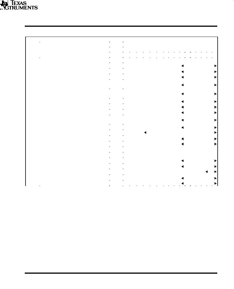
TMS320C25
SPRS010B Ð MAY 1987 Ð REVISED NOVEMBER 1990
Table 3. TMS320C25 Instruction Set Summary (continued)
T REGISTER, P REGISTER, AND MULTIPLY INSTRUCTIONS
MNEMONIC |
DESCRIPTION |
NO. |
|
|
|
|
|
INSTRUCTION BIT CODE |
|
|
|
|
|
|
|
|||||||||
WORDS |
|
|
|
|
|
|
|
|
|
|
|
|
|
|
|
|
|
|
|
|
|
|||
|
|
|
|
|
|
|
|
|
|
|
|
|
|
|
|
|
|
|
|
|
|
|
|
|
|
|
|
15 |
14 |
13 |
12 |
11 |
10 |
9 |
8 |
7 |
6 |
5 |
4 |
3 |
2 |
1 |
0 |
||||||
|
|
|
|
|||||||||||||||||||||
|
|
|
|
|
|
|
|
|
|
|
|
|
|
|
|
|
|
|
||||||
APAC |
Add P register to accumulator |
1 |
1 |
1 |
0 |
0 |
1 |
1 |
1 |
0 |
0 |
0 |
0 |
1 |
0 |
1 |
0 |
1 |
||||||
LPH² |
Load high P register |
1 |
0 |
1 |
0 |
1 |
0 |
0 |
1 |
1 |
I |
|
|
|
|
D |
|
|
|
|
|
|||
|
|
|
|
|
|
|
|
|
||||||||||||||||
LT |
Load T register |
1 |
0 |
0 |
1 |
1 |
1 |
1 |
0 |
0 |
I |
|
|
|
|
D |
|
|
|
|
|
|||
|
|
|
|
|
|
|
|
|
||||||||||||||||
LTA |
Load T register and accumulate previous product |
1 |
0 |
0 |
1 |
1 |
1 |
1 |
0 |
1 |
I |
|
|
|
|
D |
|
|
|
|
|
|||
|
|
|
|
|
|
|
|
|
||||||||||||||||
LTD |
Load T register, accumulate previous product, |
1 |
0 |
0 |
1 |
1 |
1 |
1 |
1 |
1 |
I |
|
|
|
|
D |
|
|
|
|
|
|||
and move data |
|
|
|
|
|
|
|
|
|
|||||||||||||||
|
|
|
|
|
|
|
|
|
||||||||||||||||
|
|
|
|
|
|
|
|
|
|
|
|
|
|
|
|
|
|
|
|
|
|
|||
LTP² |
Load T register and store P register in |
1 |
0 |
0 |
1 |
1 |
1 |
1 |
1 |
0 |
I |
|
|
|
|
D |
|
|
|
|
|
|||
accumulator |
|
|
|
|
|
|
|
|
|
|
||||||||||||||
|
|
|
|
|
|
|
|
|
|
|
|
|
|
|
|
|
|
|
|
|
|
|
|
|
LTS² |
Load T register and subtract previous product |
1 |
0 |
1 |
0 |
1 |
1 |
0 |
1 |
1 |
I |
|
|
|
|
D |
|
|
|
|
|
|||
|
|
|
|
|
|
|
|
|
||||||||||||||||
MAC² |
Multiply and accumulate |
2 |
0 |
1 |
0 |
1 |
1 |
1 |
0 |
1 |
I |
|
|
|
|
D |
|
|
|
|
|
|||
|
|
|
|
|
|
|
|
|
||||||||||||||||
MACD² |
Multiply and accumulate with data move |
2 |
0 |
1 |
0 |
1 |
1 |
1 |
0 |
0 |
I |
|
|
|
|
D |
|
|
|
|
|
|||
|
|
|
|
|
|
|
|
|
||||||||||||||||
MPY |
Multiply (with T register, store product in |
1 |
0 |
0 |
1 |
1 |
1 |
0 |
0 |
0 |
I |
|
|
|
|
D |
|
|
|
|
|
|||
P register) |
|
|
|
|
|
|
|
|
|
|
||||||||||||||
|
|
|
|
|
|
|
|
|
|
|||||||||||||||
|
|
|
|
|
|
|
|
|
|
|
|
|
|
|
|
|
|
|
|
|
|
|
|
|
MPYA³ |
Multiply and accumulate previous product |
1 |
0 |
0 |
1 |
1 |
1 |
0 |
1 |
0 |
I |
|
|
|
|
D |
|
|
|
|
|
|||
|
|
|
|
|
|
|
|
|
||||||||||||||||
MPYK |
Multiply immediate |
1 |
1 |
0 |
1 |
|
|
|
|
|
|
|
|
K |
|
|
|
|
|
|
|
|
|
|
|
|
|
|
|
|
|
|
|
|
|
|
|
|
|
|
|
||||||||
MPYS³ |
|
|
|
|
|
|
|
|
|
|
|
|
|
|
|
|
|
|
|
|
|
|
||
Multiply and subtract previous product |
1 |
0 |
0 |
1 |
1 |
1 |
0 |
1 |
1 |
I |
|
|
|
|
D |
|
|
|
|
|
||||
|
|
|
|
|
|
|
|
|
||||||||||||||||
MPYU³ |
Multiply unsigned |
1 |
1 |
1 |
0 |
0 |
1 |
1 |
1 |
1 |
I |
|
|
|
|
D |
|
|
|
|
|
|||
|
|
|
|
|
|
|
|
|
||||||||||||||||
PAC |
Load accumulator with P register |
1 |
1 |
1 |
0 |
0 |
1 |
1 |
1 |
0 |
0 |
0 |
0 |
1 |
0 |
1 |
0 |
0 |
||||||
SPAC |
Subtract P register from accumulator |
1 |
1 |
1 |
0 |
0 |
1 |
1 |
1 |
0 |
0 |
0 |
0 |
1 |
0 |
1 |
1 |
0 |
||||||
SPH³ |
Store high P register |
1 |
0 |
1 |
1 |
1 |
1 |
1 |
0 |
1 |
I |
|
|
|
|
D |
|
|
|
|
|
|||
|
|
|
|
|
|
|
|
|
||||||||||||||||
SPL³ |
Store low P register |
1 |
0 |
1 |
1 |
1 |
1 |
1 |
0 |
0 |
I |
|
|
|
|
D |
|
|
|
|
|
|||
|
|
|
|
|
|
|
|
|
||||||||||||||||
SPM² |
Set P register output shift mode |
1 |
1 |
1 |
0 |
0 |
1 |
1 |
1 |
0 |
0 |
0 |
0 |
0 |
1 |
0 |
|
PM |
|
|
||||
|
|
|||||||||||||||||||||||
SQRA² |
Square and accumulate |
1 |
0 |
0 |
1 |
1 |
1 |
0 |
0 |
1 |
I |
|
|
|
|
D |
|
|
|
|
|
|||
|
|
|
|
|
|
|
|
|
||||||||||||||||
|
|
|
|
|
|
|
|
|
|
|
|
|
|
|
|
|
|
|
|
|
|
|
|
|
SQRS² |
Square and subtract previous product |
1 |
0 |
1 |
0 |
1 |
1 |
0 |
1 |
0 |
I |
|
|
|
|
D |
|
|
|
|
|
|||
|
|
|
|
|
|
|
|
|
||||||||||||||||
² These instructions are not included in the TMS320C1x instruction set. ³ These instructions are not included in the TMS32020 instruction set.
14 |
POST OFFICE BOX 1443 • HOUSTON, TEXAS 77001 |
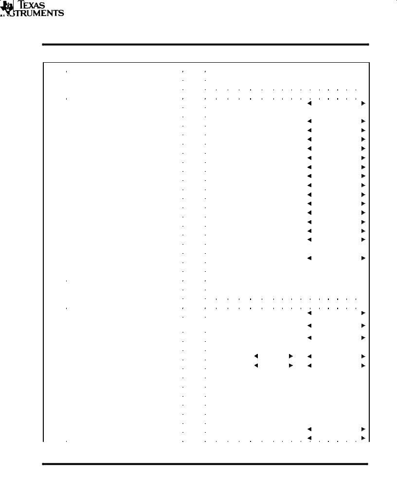
TMS320C25
SPRS010B Ð MAY 1987 Ð REVISED NOVEMBER 1990
Table 3. TMS320C25 Instruction Set Summary (continued)
BRANCH/CALL INSTRUCTIONS
MNEMONIC |
DESCRIPTION |
NO. |
|
|
|
|
|
INSTRUCTION BIT CODE |
|
|
|
|
|
|
|
|
||||||
|
|
|
|
|
|
|
|
|
|
|
|
|
|
|
|
|
|
|
||||
WORDS |
|
|
|
|
|
|
|
|
|
|
|
|
|
|
|
|
|
|
|
|||
|
|
|
15 |
14 |
13 |
12 |
11 |
10 |
9 |
8 |
7 |
6 |
5 |
4 |
3 |
2 |
1 |
0 |
||||
|
|
|
|
|||||||||||||||||||
|
|
|
|
|
|
|
|
|
|
|
|
|
|
|
|
|
|
|
|
|
|
|
B |
Branch unconditionally |
2 |
1 |
1 |
1 |
1 |
1 |
1 |
1 |
1 |
1 |
|
|
|
|
|
D |
|
|
|
|
|
|
|
|
|
|
|
|
|
|
||||||||||||||
BACC² |
Branch to address specified by accumulator |
1 |
1 |
1 |
0 |
0 |
1 |
1 |
1 |
0 |
0 |
0 |
1 |
0 |
0 |
1 |
0 |
1 |
||||
BANZ |
Branch on auxiliary register not zero |
2 |
1 |
1 |
1 |
1 |
1 |
0 |
1 |
1 |
1 |
|
|
|
|
|
D |
|
|
|
|
|
|
|
|
|
|
|
|
|
|
||||||||||||||
BBNZ² |
Branch if TC bit ≠ 0 |
2 |
1 |
1 |
1 |
1 |
1 |
0 |
0 |
1 |
1 |
|
|
|
|
|
D |
|
|
|
|
|
|
|
|
|
|
|
|
|
|
||||||||||||||
BBZ² |
Branch if TC bit = 0 |
2 |
1 |
1 |
1 |
1 |
1 |
0 |
0 |
0 |
1 |
|
|
|
|
|
D |
|
|
|
|
|
|
|
|
|
|
|
|
|
|
||||||||||||||
BC³ |
Branch on carry |
2 |
0 |
1 |
0 |
1 |
1 |
1 |
1 |
0 |
1 |
|
|
|
|
|
D |
|
|
|
|
|
|
|
|
|
|
|
|
|
|
||||||||||||||
BGEZ |
Branch if accumulator ≥ 0 |
2 |
1 |
1 |
1 |
1 |
0 |
1 |
0 |
0 |
1 |
|
|
|
|
|
D |
|
|
|
|
|
|
|
|
|
|
|
|
|
|
||||||||||||||
BGZ |
Branch if accumulator > 0 |
2 |
1 |
1 |
1 |
1 |
0 |
0 |
0 |
1 |
1 |
|
|
|
|
|
D |
|
|
|
|
|
|
|
|
|
|
|
|
|
|
||||||||||||||
BIOZ |
Branch on I/O status = 0 |
2 |
1 |
1 |
1 |
1 |
1 |
0 |
1 |
0 |
1 |
|
|
|
|
|
D |
|
|
|
|
|
|
|
|
|
|
|
|
|
|
||||||||||||||
BLEZ |
Branch if accumulator ≤ 0 |
2 |
1 |
1 |
1 |
1 |
0 |
0 |
1 |
0 |
1 |
|
|
|
|
|
D |
|
|
|
|
|
|
|
|
|
|
|
|
|
|
||||||||||||||
BLZ |
Branch if accumulator < 0 |
2 |
1 |
1 |
1 |
1 |
0 |
0 |
1 |
1 |
1 |
|
|
|
|
|
D |
|
|
|
|
|
|
|
|
|
|
|
|
|
|
||||||||||||||
BNC³ |
Branch on no carry |
2 |
0 |
1 |
0 |
1 |
1 |
1 |
1 |
1 |
1 |
|
|
|
|
|
D |
|
|
|
|
|
|
|
|
|
|
|
|
|
|
||||||||||||||
BNV² |
Branch if no overflow |
2 |
1 |
1 |
1 |
1 |
0 |
1 |
1 |
1 |
1 |
|
|
|
|
|
D |
|
|
|
|
|
|
|
|
|
|
|
|
|
|
||||||||||||||
BNZ |
Branch if accumulator ≠ 0 |
2 |
1 |
1 |
1 |
1 |
0 |
1 |
0 |
1 |
1 |
|
|
|
|
|
D |
|
|
|
|
|
|
|
|
|
|
|
|
|
|
||||||||||||||
BV |
Branch on overflow |
2 |
1 |
1 |
1 |
1 |
0 |
0 |
0 |
0 |
1 |
|
|
|
|
|
D |
|
|
|
|
|
|
|
|
|
|
|
|
|
|
||||||||||||||
BZ |
Branch if accumulator = 0 |
2 |
1 |
1 |
1 |
1 |
0 |
1 |
1 |
0 |
1 |
|
|
|
|
|
D |
|
|
|
|
|
|
|
|
|
|
|
|
|
|
||||||||||||||
CALA |
Call subroutine indirect |
1 |
1 |
1 |
0 |
0 |
1 |
1 |
1 |
0 |
0 |
0 |
1 |
0 |
0 |
1 |
0 |
0 |
||||
CALL |
Call subroutine |
2 |
1 |
1 |
1 |
1 |
1 |
1 |
1 |
0 |
1 |
|
|
|
|
|
D |
|
|
|
|
|
|
|
|
|
|
|
|
|
|
||||||||||||||
RET |
Return from subroutine |
1 |
1 |
1 |
0 |
0 |
1 |
1 |
1 |
0 |
0 |
0 |
1 |
0 |
0 |
1 |
1 |
0 |
||||
|
|
|
|
|
|
|
|
|
|
|
|
|
|
|
|
|
|
|
|
|
|
|
I/O AND DATA MEMORY OPERATIONS
MNEMONIC |
DESCRIPTION |
NO. |
|
|
|
|
|
|
INSTRUCTION BIT CODE |
|
|
|
|
|
|
|
|
|||||||
WORDS |
|
|
|
|
|
|
|
|
|
|
|
|
|
|
|
|
|
|
|
|
|
|||
|
|
|
15 |
14 |
13 |
12 |
11 |
10 |
9 |
8 |
7 |
6 |
5 |
4 |
3 |
2 |
1 |
0 |
||||||
|
|
|
|
|||||||||||||||||||||
|
|
|
|
|
|
|
|
|
|
|
|
|
|
|
|
|
|
|
|
|
|
|
||
BLKD² |
Block move from data memory to data memory |
2 |
1 |
1 |
1 |
0 |
1 |
1 |
|
0 |
1 |
I |
|
|
|
|
|
D |
|
|
|
|
||
|
|
|
|
|
|
|
|
|
||||||||||||||||
BLKP² |
Block move from program memory to data |
2 |
1 |
1 |
1 |
1 |
1 |
1 |
|
0 |
0 |
I |
|
|
|
|
|
D |
|
|
|
|
||
memory |
|
|
|
|
|
|
|
|
|
|
|
|||||||||||||
|
|
|
|
|
|
|
|
|
|
|||||||||||||||
|
|
|
|
|
|
|
|
|
|
|
|
|
|
|
|
|
|
|
|
|
|
|
|
|
DMOV |
Data move in data memory |
1 |
0 |
1 |
0 |
1 |
0 |
1 |
|
1 |
0 |
I |
|
|
|
|
|
D |
|
|
|
|
||
|
|
|
|
|
|
|
|
|
||||||||||||||||
FORT² |
Format serial port registers |
1 |
1 |
1 |
0 |
0 |
1 |
1 |
|
1 |
0 |
0 |
0 |
0 |
0 |
1 |
1 |
1 |
FO |
|||||
IN |
Input data from port |
1 |
1 |
0 |
0 |
0 |
|
|
|
|
|
|
I |
|
|
|
|
|
|
|
|
|
|
|
|
|
|
|
PA |
|
|
|
|
|
|
D |
|
|
|
|
|||||||||
|
|
|
|
|
|
|
|
|
|
|
|
|
|
|||||||||||
OUT |
Output data to port |
1 |
1 |
1 |
1 |
0 |
|
|
|
|
|
|
I |
|
|
|
|
|
|
|
|
|
|
|
|
|
|
|
PA |
|
|
|
|
|
|
D |
|
|
|
|
|||||||||
|
|
|
|
|
|
|
|
|
|
|
|
|
|
|||||||||||
RFSM³ |
|
|
|
|
|
|
|
|
|
|
|
|
|
|
|
|
|
|
|
|||||
Reset serial port frame synchronization mode |
1 |
1 |
1 |
0 |
0 |
1 |
1 |
|
1 |
0 |
0 |
0 |
1 |
1 |
0 |
1 |
1 |
0 |
||||||
RTXM² |
Reset serial port transmit mode |
1 |
1 |
1 |
0 |
0 |
1 |
1 |
|
1 |
0 |
0 |
0 |
1 |
0 |
0 |
0 |
0 |
0 |
|||||
RXF² |
Reset external flag |
1 |
1 |
1 |
0 |
0 |
1 |
1 |
|
1 |
0 |
0 |
0 |
0 |
0 |
1 |
1 |
0 |
0 |
|||||
SFSM³ |
Set serial port frame synchronization mode |
1 |
1 |
1 |
0 |
0 |
1 |
1 |
|
1 |
0 |
0 |
0 |
1 |
1 |
0 |
1 |
1 |
1 |
|||||
STXM² |
Set serial port transmit mode |
1 |
1 |
1 |
0 |
0 |
1 |
1 |
|
1 |
0 |
0 |
0 |
1 |
0 |
0 |
0 |
0 |
1 |
|||||
SXF² |
Set external flag |
1 |
1 |
1 |
0 |
0 |
1 |
1 |
|
1 |
0 |
0 |
0 |
0 |
0 |
1 |
1 |
0 |
1 |
|||||
TBLR |
Table read |
|
1 |
0 |
1 |
0 |
1 |
1 |
0 |
|
0 |
0 |
I |
|
|
|
|
|
D |
|
|
|
|
|
|
|
|
|
|
|
|
|
|
|
|||||||||||||||
TBLW |
Table write |
|
1 |
0 |
1 |
0 |
1 |
1 |
0 |
|
0 |
1 |
I |
|
|
|
|
|
D |
|
|
|
|
|
|
|
|
|
|
|
|
|
|
|
|||||||||||||||
² These instructions are not included in the TMS320C1x instruction set. ³ These instructions are not included in the TMS32020 instruction set.
POST OFFICE BOX 1443 • HOUSTON, TEXAS 77001 |
15 |

TMS320C25
SPRS010B Ð MAY 1987 Ð REVISED NOVEMBER 1990
Table 3. TMS320C25 Instruction Set Summary (concluded)
CONTROL INSTRUCTIONS
MNEMONIC |
DESCRIPTION |
NO. |
|
|
|
|
INSTRUCTION BIT CODE |
|
|
|
|
|
|
||||||||||
WORDS |
|
|
|
|
|
|
|
|
|
|
|
|
|
|
|
|
|
|
|
|
|
||
|
|
|
|
|
|
|
|
|
|
|
|
|
|
|
|
|
|
|
|
|
|
|
|
|
|
15 |
14 |
13 |
12 |
11 |
10 |
9 |
8 |
7 |
6 |
5 |
4 |
3 |
2 |
1 |
0 |
||||||
|
|
|
|||||||||||||||||||||
|
|
|
|
|
|
|
|
|
|
|
|
|
|
|
|
|
|
|
|
|
|
|
|
BIT² |
Test bit |
1 |
1 |
0 |
0 |
1 |
|
|
|
B |
|
|
|
I |
|
|
|
|
|
D |
|
|
|
|
|
|
|
|
|
|
|
|
|
|
|
|
|
||||||||||
BITT² |
Test bit specified by T register |
1 |
0 |
1 |
0 |
1 |
0 |
1 |
1 |
1 |
I |
|
|
|
|
|
D |
|
|
|
|||
|
|
|
|
|
|
|
|
||||||||||||||||
CNFD² |
Configure block as data memory |
1 |
1 |
1 |
0 |
0 |
1 |
1 |
1 |
0 |
0 |
0 |
0 |
0 |
0 |
1 |
0 |
0 |
|||||
CNFP² |
Configure block as program memory |
1 |
1 |
1 |
0 |
0 |
1 |
1 |
1 |
0 |
0 |
0 |
0 |
0 |
0 |
1 |
0 |
1 |
|||||
DINT |
Disable interrupt |
1 |
1 |
1 |
0 |
0 |
1 |
1 |
1 |
0 |
0 |
0 |
0 |
0 |
0 |
0 |
0 |
1 |
|||||
EINT |
Enable interrupt |
1 |
1 |
1 |
0 |
0 |
1 |
1 |
1 |
0 |
0 |
0 |
0 |
0 |
0 |
0 |
0 |
0 |
|||||
IDLE² |
Idle until interrupt |
1 |
1 |
1 |
0 |
0 |
1 |
1 |
1 |
0 |
0 |
0 |
0 |
1 |
1 |
1 |
1 |
1 |
|||||
LST |
Load status register STO |
1 |
0 |
1 |
0 |
1 |
0 |
0 |
0 |
0 |
I |
|
|
|
|
|
D |
|
|
|
|||
|
|
|
|
|
|
|
|
||||||||||||||||
LST1² |
Load status register ST1 |
1 |
0 |
1 |
0 |
1 |
0 |
0 |
0 |
1 |
I |
|
|
|
|
|
D |
|
|
|
|||
|
|
|
|
|
|
|
|
||||||||||||||||
NOP |
No operation |
1 |
0 |
1 |
0 |
1 |
0 |
1 |
0 |
1 |
0 |
0 |
0 |
0 |
0 |
0 |
0 |
0 |
|||||
POP |
Pop top of stack to low accumulator |
1 |
1 |
1 |
0 |
0 |
1 |
1 |
1 |
0 |
0 |
0 |
0 |
1 |
1 |
1 |
0 |
1 |
|||||
POPD² |
Pop top of stack to data memory |
1 |
0 |
1 |
1 |
1 |
1 |
0 |
1 |
0 |
I |
|
|
|
|
|
D |
|
|
|
|||
|
|
|
|
|
|
|
|
||||||||||||||||
PSHD² |
Push data memory value onto stack |
1 |
0 |
1 |
0 |
1 |
0 |
1 |
0 |
0 |
I |
|
|
|
|
|
D |
|
|
|
|||
|
|
|
|
|
|
|
|
||||||||||||||||
PUSH |
Push low accumulator onto stack |
1 |
1 |
1 |
0 |
0 |
1 |
1 |
1 |
0 |
0 |
0 |
0 |
1 |
1 |
1 |
0 |
0 |
|||||
RC³ |
Reset carry bit |
1 |
1 |
1 |
0 |
0 |
1 |
1 |
1 |
0 |
0 |
0 |
1 |
1 |
0 |
0 |
0 |
0 |
|||||
RHM³ |
Reset hold mode |
1 |
1 |
1 |
0 |
0 |
1 |
1 |
1 |
0 |
0 |
0 |
1 |
1 |
1 |
0 |
0 |
0 |
|||||
ROVM |
Reset overflow mode |
1 |
1 |
1 |
0 |
0 |
1 |
1 |
1 |
0 |
0 |
0 |
0 |
0 |
0 |
0 |
1 |
0 |
|||||
RPT² |
Repeat instruction as specified by data |
1 |
0 |
1 |
0 |
0 |
1 |
0 |
1 |
1 |
I |
|
|
|
|
|
D |
|
|
|
|||
memory value |
|
|
|
|
|
|
|
|
|||||||||||||||
|
|
|
|
|
|
|
|
||||||||||||||||
|
|
|
|
|
|
|
|
|
|
|
|
|
|
|
|
|
|
|
|
|
|
|
|
RPTK² |
Repeat instruction as specified by immediate |
1 |
1 |
1 |
0 |
0 |
1 |
0 |
1 |
1 |
|
|
|
|
|
K |
|
|
|
|
|||
value |
|
|
|
|
|
|
|
|
|
||||||||||||||
|
|
|
|
|
|
|
|
|
|||||||||||||||
|
|
|
|
|
|
|
|
|
|
|
|
|
|
|
|
|
|
|
|
|
|
|
|
RSXM² |
Reset sign-extension mode |
1 |
1 |
1 |
0 |
0 |
1 |
1 |
1 |
0 |
0 |
0 |
0 |
0 |
0 |
1 |
1 |
0 |
|||||
RTC³ |
Reset test/control flag |
1 |
1 |
1 |
0 |
0 |
1 |
1 |
1 |
0 |
0 |
0 |
1 |
1 |
0 |
0 |
1 |
0 |
|||||
SC³ |
Set carry bit |
1 |
1 |
1 |
0 |
0 |
1 |
1 |
1 |
0 |
0 |
0 |
1 |
1 |
0 |
0 |
0 |
1 |
|||||
SHM³ |
Set hold mode |
1 |
1 |
1 |
0 |
0 |
1 |
1 |
1 |
0 |
0 |
0 |
1 |
1 |
1 |
0 |
0 |
1 |
|||||
SOVM |
Set overflow mode |
1 |
1 |
1 |
0 |
0 |
1 |
1 |
1 |
0 |
0 |
0 |
0 |
0 |
0 |
0 |
1 |
1 |
|||||
SST |
Store status register ST0 |
1 |
0 |
1 |
1 |
1 |
1 |
0 |
0 |
0 |
I |
|
|
|
|
|
D |
|
|
|
|||
SST1² |
Store status register ST1 |
1 |
0 |
1 |
1 |
1 |
1 |
0 |
0 |
1 |
I |
|
|
|
|
|
|
|
|
||||
|
|
|
|
|
D |
|
|
|
|||||||||||||||
|
|
|
|
|
|
|
|
||||||||||||||||
|
|
|
|
|
|
|
|
|
|
|
|
|
|
|
|
|
|
|
|
|
|
|
|
SSXM² |
Set sign-extension mode |
1 |
1 |
1 |
0 |
0 |
1 |
1 |
1 |
0 |
0 |
0 |
0 |
0 |
0 |
1 |
1 |
1 |
|||||
STC³ |
Set test/control flag |
1 |
1 |
1 |
0 |
0 |
1 |
1 |
1 |
0 |
0 |
0 |
1 |
1 |
0 |
0 |
1 |
1 |
|||||
TRAP² |
Software interrupt |
1 |
1 |
1 |
0 |
0 |
1 |
1 |
1 |
0 |
0 |
0 |
0 |
1 |
1 |
1 |
1 |
0 |
|||||
² These instructions are not included in the TMS320C1x instruction set.
³ These instructions are not included in the TMS32020 instruction set.
16 |
POST OFFICE BOX 1443 • HOUSTON, TEXAS 77001 |

TMS32020
SPRS010B Ð MAY 1987 Ð REVISED NOVEMBER 1990
TMS32020 PRODUCT NOTIFICATION
Texas Instruments has identified an unusual set of circumstances that will cause the BIT (Test Bit) instruction on the TMS32020 to affect the contents of the accumulator; ideally, the BIT instruction should not affect the accumulator. This set of conditions is:
1.The overflow mode is set (the OVM status register bit is set to one.)
2.And, the two LSBs of the BIT instruction opcode word are zero.
a.When direct memory addressing is used, every fourth data word is affected; all other locations are not affected.
b.When indirect addressing is used, the two LSBs will be zero if a new ARP is not selected or if a new ARP is selected and that ARP is 0 or 4.
3.And, adding the contents of the accumulator with the contents of the addressed data memory location, shifted by 2 (bit code), causes an overflow of the accumulator.
If all of these conditions are met, the contents of the accumulator will be replaced by the positive or negative saturation value, depending on the polarity of the overflow.
Various methods for avoiding this phenomenon are available:
•If the TMS32020 is not in the saturation mode when the BIT instruction is executed, the device operates properly and the accumulator is not affected.
•Execute the Reset Overflow Mode (ROVM) instruction immediately prior to the BIT instruction and the Set Overflow Mode (SOVM) instruction immediately following the BIT instruction.
•If direct memory addressing is being used during the BIT instructions, reorganize memory so that the page relative locations 0, 4, 8, C, 10 . . . are not used.
•If indirect addressing is being used during the Bit instruction, select a new ARP which is not AR0 or AR4. If necessary, follow the instruction with a LARP AR0 or LARP AR4 to restore the code.
•Use the Test Bit Specified by T Register (BITT) instruction instead of the BIT instruction. The BITT instruction operates correctly and will not affect the accumulator under any circumstances.
•Replace TMS32020 with TMS320C25 for ideal pin-to-pIn and object-code compatibility. The BIT instruction on the TMS320C25 executes properly and will not affect the accumulator under any circumstances.
POST OFFICE BOX 1443 • HOUSTON, TEXAS 77001 |
17 |

TMS320 SECOND-GENERATION
DEVICES
SPRS010B Ð MAY 1987 Ð REVISED NOVEMBER 1990
development support
Together, Texas Instruments and its authorized third-party suppliers offer an extensive line of development support products to assist the user in all aspects of TMS320 second-generation-based design and development. These products range from development and application software to complete hardware development and evaluation systems. Table 4 lists the development support products for the second-generation TMS320 devices.
System development may begin with the use of the simulator, Software Development System (SWDS), or emulator (XDS) along with an assembler/linker. These tools give the TMS320 user various means of evaluation, from software simulation of the second-generation TMS320s (simulator) to full-speed in-circuit emulation with hardware and software breakpoint trace and timing capabilities (XDS).
Software and hardware can be developed simultaneously by using the macro assembler/linker, C compiler, and simulator for software development, the XDS for hardware development, and the Software Development System for both software development and limited hardware development.
Many third-party vendors offer additional development support for the second-generation TMS320s, including assembler/linkers, simulators, high-level languages, applications software, algorithm development tools, application boards, software development boards, and in-circuit emulators. Refer to the TMS320 Family Development Support Reference Guide (SPRU011A) for further information about TMS320 development support products offered by both Texas Instruments and its third-party suppliers.
Additional support for the TMS320 products consists of an extensive library or product and applications documentation. Three-day DSP design workshops are offered by the TI Regional Technology Centers (RTCs). These workshops provide insight into the architecture and the instruction set of the second-generation TMS320s as well as hands-on training with the TMS320 development tools. When technical questions arise regarding the TMS320 family, contact the Texas Instruments TMS320 Hotline at (713) 274-2320. Or, keep informed on the latest TI and third-party development support tools by accessing the DSP Bulletin Board Service (BBS) at (713) 274-2323. The BBS serves 2400-, 1200and 300-bps modems. Also, TMS320 application source code may be downloaded from the BBS.
18 |
POST OFFICE BOX 1443 • HOUSTON, TEXAS 77001 |

TMS320 SECOND-GENERATION
DEVICES
SPRS010B Ð MAY 1987 Ð REVISED NOVEMBER 1990
Table 4. TMS320 Second-Generation Software and Hardware Support
SOFTWARE TOOLS |
PART NUMBER |
|
|
|
|
Macro Assembler/Linker |
|
|
IBM MS/PC-DOS |
TMDS3242850-02 |
|
VAX/VMS |
TMDS3242250-08 |
|
VAX ULTRIX |
TMDS3242260-08 |
|
SUN UNIX |
TMDS3242550-08 |
|
Simulator |
|
|
IBM MS/PC-DOS |
TMDS3242851-02 |
|
VAX/VMS |
TMDS3242251-08 |
|
C Compiler |
|
|
IBM MS/PC-DOS |
TMDX3242855-02 |
|
VAX/VMS |
TMDX3242255-08 |
|
VAX ULTRIX |
TMDX3242265-08 |
|
SUN UNIX |
TMDX3242555-08 |
|
Digital Filter Design Package (DFDP) |
|
|
IBM PC-DOS |
DFDP-IBM002 |
|
DSP Software Library |
|
|
IBM MS/PC-DOS |
TMDC3240812-12 |
|
VAX/VMS |
TMDC3204212-18 |
|
|
|
|
HARDWARE TOOLS |
PART NUMBER |
|
|
|
|
Analog Interface Board 2 (AIB2) |
RTC/AIB320A-06 |
|
Analog Interface Board Adaptor |
RTC/ADP320A-06 |
|
EPROM Programmer Adaptor Socket |
TMDX3270120 |
|
(68 to 28-pin) |
||
|
||
Software Development System (SWDS) |
TMDX3268821 |
|
XDS/22 Emulator (see Note) |
TMDS3262221 |
|
XDS/22 Upgrade (TMS32020 to TMS320C2x) |
TMDX3282226 |
NOTE: Emulation support for the TMS320C25-50 is available from Macrochip
Research, Inc.; refer to the TMS320 Family Development Support Reference
Guide (SPRU011A) for the mailing address.
IBM is a trademark of International Business Machines Corporation.
PC-DOS is a trademark of International Business Machines Corporation.
VAX and VMS are trademarks of Digital Equipment Corporation.
XDS is a trademark of Texas Instruments Incorporated.
POST OFFICE BOX 1443 • HOUSTON, TEXAS 77001 |
19 |

TMS320 SECOND-GENERATION
DEVICES
SPRS010B Ð MAY 1987 Ð REVISED NOVEMBER 1990
documentation support
Extensive documentation supports the second-generation TMS320 devices from product announcement through applications development. The types of documentation include data sheets with design specifications, complete user's guides, and 750 pages of application reports published in the book, Digital Signal Processing Applications with the TMS320 Family (SPRA012A). An application report, Hardware Interfacing to the TMS320C25 (SPRA014A), is available for that device.
A series of DSP textbooks is being published by Prentice-Hall and John Wiley & Sons to support digital signal processing research and education. The TMS320 newsletter, Details on Signal Processing, is published quarterly and distributed to update TMS320 customers on product information. The TMS320 DSP bulletin board service provides access to large amounts of information pertaining to the TMS320 family.
Refer to the TMS320 Family Development Support Reference Guide (SPRU011A) for further information about TMS320 documentation. To receive copies of second-generation TMS320 literature, call the Customer Response Center at 1-800-232-3200.
specification overview
The electrical specifications for the TMS32020, TMS320C25, TMS320E25, and TMS320C25-50 are given in the following pages. Note that the electrical specifications for the TMS320E25 are identical to those for the TMS320C25, with the addition of EPROM-related specifications. A summary of differences between TMS320C25 and TMS320C25-50 specifications immediately follows the TMS320C25-50 specification.
20 |
POST OFFICE BOX 1443 • HOUSTON, TEXAS 77001 |
TMS32020
SPRS010B Ð MAY 1987 Ð REVISED NOVEMBER 1990
absolute maximum ratings over specified temperature range (unless otherwise noted)²
Supply voltage range, VCC³ . . . . . . . . . . . . . . . . . . . . . . . . . . . . . . . . . . . . . . . . . . . . . . . . . . . . . . . |
. ± 0.3 |
V to 7 V |
Input voltage range . . . . . . . . . . . . . . . . . . . . . . . . . . . . . . . . . . . . . . . . . . . . . . . . . . . . . . . . . . . . . . . |
± 0.3 |
V to 7 V |
Output voltage range . . . . . . . . . . . . . . . . . . . . . . . . . . . . . . . . . . . . . . . . . . . . . . . . . . . . . . . . . . . . . . |
± 0.3 |
V to 7 V |
Continuous power dissipation . . . . . . . . . . . . . . . . . . . . . . . . . . . . . . . . . . . . . . . . . . . . . . . . . . . . . . |
. . . . . . . |
. . 2 W |
Operating free-air temperature range . . . . . . . . . . . . . . . . . . . . . . . . . . . . . . . . . . . . . . . . . . . . . . . . |
. . 0°C to 70°C |
|
Storage temperature range . . . . . . . . . . . . . . . . . . . . . . . . . . . . . . . . . . . . . . . . . . . . . . . . . . . . . . . |
± 55°C to 150°C |
|
²Stresses beyond those listed under ªAbsolute Maximum Ratingsº may cause permanent damage to the device. This is a stress ratingonly, and functional operation of the device at these or any other conditions beyond those indicated in the ªRecommended Operating Conditionsº section of
this specification is not implied. Exposure to absolute-maximum-rated conditions for extended periods may affect device reliability. ³ All voltage values are with respect to VSS.
recommended operating conditions
|
|
|
MIN |
NOM |
MAX |
UNIT |
|
|
|
|
|
|
|
|
|
VCC |
Supply voltage |
4.75 |
5 |
5.25 |
V |
||
VSS |
Supply voltage |
|
0 |
|
V |
||
VIH |
High-level input voltage |
All inputs except CLKIN |
2 |
VCC + 0.3 |
V |
||
CLKIN |
2.4 |
VCC + 0.3 |
V |
||||
|
|
||||||
VIL |
Low-level input voltage |
All inputs except CLKIN |
± 0.3 |
|
0.8 |
V |
|
|
|
|
|
|
|||
CLKIN |
± 0.3 |
|
0.8 |
V |
|||
|
|
|
|||||
|
|
|
|
|
|
|
|
IOH |
High-level output current |
|
|
300 |
µA |
||
IOL |
Low-level output current |
|
|
2 |
mA |
||
TA |
Operating free-air temperature (see Notes 1 and 2) |
0 |
|
70 |
°C |
||
NOTES: 1. Case temperature (TC) must be maintained below 90°C. 2. RθJA = 36°C/Watt, RθJC = 6°C/Watt.
electrical characteristics over specified free-air temperature range (unless otherwise noted)
|
PARAMETER |
TEST CONDITIONS |
MIN |
TYP§ |
MAX |
UNIT |
VOH |
High-level output voltage |
VCC = MIN, IOH = MAX |
2.4 |
3 |
|
V |
VOL |
Low-level output voltage |
VCC = MIN, IOL = MAX |
|
0.3 |
0.6 |
V |
IZ |
Three-state current |
VCC = MAX |
±20 |
|
20 |
µA |
II |
Input current |
VI = VSS to VCC |
±10 |
|
10 |
µA |
|
|
TA = 0°C, VCC = MAX, fx = MAX |
|
|
360 |
mA |
ICC |
Supply current |
TA = 25°C, VCC = MAX, fx = MAX |
|
250 |
|
mA |
|
|
TC = 90°C, VCC = MAX, fx = MAX |
|
|
285 |
mA |
CI |
Input capacitance |
|
|
|
15 |
pF |
CO |
Output capacitance |
|
|
|
15 |
pF |
§ All typical values for ICC are at VCC = 5 V, TA = 25°C.
This device contains circuits to protect its inputs and outputs against damage due to high static voltages or electrostatic fields. These circuits have been qualified to protect this device against electrostatic discharges (ESD) of up to 2 kV according to MIL-STD-883C, Method 3015; however, it is advised that precautions should be taken to avoid application of any voltage higher than maximum-rated voltages to these high-impedance circuits. During storage or handling, the device leads should be shorted together or the device
should be placed in conductive foam. In a circuit, unused inputs should always be connected to an appropriated logic voltage level, preferably either
VCC or ground. Specific guidelines for handling devices of this type are contained in the publication Guidelines for Handling Electrostatic-Discharge-Sensitive (ESDS) Devices and Assemblies available from Texas Instruments.
ADVANCE INFORMATION
POST OFFICE BOX 1443 • HOUSTON, TEXAS 77001 |
21 |
 Loading...