


Service Manual
TDS 310, TDS 320 & TDS 350
Two Channel Oscilloscopes
070-8570-05
Warning
The servicing instructions are for use by qualified personnel only. To avoid personal injury, do not perform any servicing unless you are qualified to do so. Refer to the Safety Summary prior to performing service.
This document applies for TDS 310, TDS 320, and TDS 350 Oscilloscopes with serial numbers B040100 and above.
s m l m s
"$) *.3425-&.4 -".5'"$452&% #9 &+42/.*8 )"3 " 3&2*", .5-#&2 /. " 0".&, *.3&24 /2 4"( /2 34"-0&% /. 4)& $)"33*3 )& '*234 ,&44&2 *. 4)& 3&2*", .5-#&2 %&3*(."4&3 4)& $/5.429 /' -".5'"$452& )& ,"34 '*6& %*(*43 /' 4)& 3&2*", .5-#&2 "2& "33*(.&% 3&15&.4*",,9 ".% "2& 5.*15& 4/ &"$) *.3425-&.4 )/3& -".5'"$452&% *. 4)&.*4&% 4"4&3 )"6& 3*8 5.*15& %*(*43 )& $/5.429 /' -".5'"$452& *3 *%&.4*'*&% "3 '/,,/73
|
&+42/.*8 .$ &"6&24/. 2&(/. |
|
2 |
&+42/.*8 |
.*4&% *.(%/- 4% /.%/. |
3 |
/.9 &+42/.*8 "0". |
|
|
&+42/.*8 |
/,,".% &&2&.6&&. )& &4)&2,".%3 |
.3425-&.43 -".5'"$452&% '/2 &+42/.*8 #9 &84&2.", 6&.%/23 /543*%& 4)& .*4&% 4"4&3 "2& "33*(.&% " 47/ %*(*4 ",0)" $/%& 4/ *%&.4*'9 4)& $/5.429 /' -".5'"$452& & ( '/2 "0". '/2 /.( /.( '/2 32"&, &4$
&+42/.*8 .$ /8 &"6&24/. 9
2*.4&% *.
/092*()4 &+42/.*8 .$ 993 ,, 2*()43 2&3&26&% &+42/.*8 02/%5$43 "2& $/6&2&% #9 ".% '/2&*(. 0"4&.43 *335&% ".% 0&.%*.( )& '/,,/7*.( "2& 2&(*34&2&% 42"%&-"2+3 ! :
".% ;
WARRANTY
Tektronix warrants that this product will be free from defects in materials and workmanship for a period of three 3 years from the date of shipment If any such product proves defective during this warranty period Tektronix at its option either will repair the defective product without charge for parts and labor or will provide a replacement in exchange for the defective product
In order to obtain service under this warranty Customer must notify Tektronix of the defect before the expiration of the warranty period and make suitable arrangements for the performance of service Customer shall be responsible for packaging and shipping the defective product to the service center designated by Tektronix with shipping charges prepaid Tektronix shall pay for the return of the product to Customer if the shipment is to a location within the country in which the Tektronix service center is located Customer shall be responsible for paying all shipping charges duties taxes and any other charges for products returned to any other locations
This warranty shall not apply to any defect failure or damage caused by improper use or improper or inadequate maintenance and care Tektronix shall not be obligated to furnish service under this warranty a to repair damage resulting from attempts by personnel other than Tektronix representatives to install repair or service the product; b to repair damage resulting from improper use or connection to incompatible equipment; or c to service a product that has been modified or integrated with other products when the effect of such modification or integration increases the time or difficulty of servicing the product
THIS WARRANTY IS GIVEN BY TEKTRONIX WITH RESPECT TO THIS PRODUCT IN LIEU OF ANY OTHER WARRANTIES, EXPRESSED OR IMPLIED. TEKTRONIX AND ITS VENDORS DISCLAIM ANY IMPLIED WARRANTIES OF MERCHANTABILITY OR FITNESS FOR A PARTICULAR PURPOSE. TEKTRONIX' RESPONSIBILITY TO REPAIR OR REPLACE DEFECTIVE PRODUCTS IS THE SOLE AND EXCLUSIVE REMEDY PROVIDED TO THE CUSTOMER FOR BREACH OF THIS WARRANTY. TEKTRONIX AND ITS VENDORS WILL NOT BE LIABLE FOR ANY INDIRECT, SPECIAL, INCIDENTAL, OR CONSEQUENTIAL DAMAGES IRRESPECTIVE OF WHETHER TEKTRONIX OR THE VENDOR HAS ADVANCE NOTICE OF THE POSSIBILITY OF SUCH DAMAGES.

Table of Contents
Safety Summary . . . . . . . . . . . . . . . . . . . . . . . . . . . . . . . . . . . . . . . . . . . . . |
ix |
Specifications
Warranted Characteristics . . . . . . . . . . . . . . . . . . . . . . . . . . . . . . . . . . . |
1:3 |
Performance Conditions . . . . . . . . . . . . . . . . . . . . . . . . . . . . . . . . . . |
1:3 |
Typical Characteristics . . . . . . . . . . . . . . . . . . . . . . . . . . . . . . . . . . . . . . . |
1:7 |
Nominal Traits . . . . . . . . . . . . . . . . . . . . . . . . . . . . . . . . . . . . . . . . . . . . . . . |
1:11 |
Operating Information
Front Panel . . . . . . . . . . . . . . . . . . . . . . . . . . . . . . . . . . . . . . . . . . . . . . . . . |
2:1 |
Display and Power Controls . . . . . . . . . . . . . . . . . . . . . . . . . . . . . . |
2:2 |
Vertical Controls . . . . . . . . . . . . . . . . . . . . . . . . . . . . . . . . . . . . . . . . . |
2:3 |
Horizontal Controls . . . . . . . . . . . . . . . . . . . . . . . . . . . . . . . . . . . . . . |
2:4 |
Trigger Controls . . . . . . . . . . . . . . . . . . . . . . . . . . . . . . . . . . . . . . . . . |
2:5 |
Miscellaneous Controls . . . . . . . . . . . . . . . . . . . . . . . . . . . . . . . . . . |
2:6 |
Display Map . . . . . . . . . . . . . . . . . . . . . . . . . . . . . . . . . . . . . . . . . . . . . |
2:7 |
Inputs . . . . . . . . . . . . . . . . . . . . . . . . . . . . . . . . . . . . . . . . . . . . . . . . . . . |
2:8 |
Rear Panel . . . . . . . . . . . . . . . . . . . . . . . . . . . . . . . . . . . . . . . . . . . . . . . . . . |
2:9 |
Menu Maps . . . . . . . . . . . . . . . . . . . . . . . . . . . . . . . . . . . . . . . . . . . . . . . . . |
2:11 |
Theory of Operation
Logic Conventions . . . . . . . . . . . . . . . . . . . . . . . . . . . . . . . . . . . . . . . |
3:1 |
Module Interconnection . . . . . . . . . . . . . . . . . . . . . . . . . . . . . . . . . . |
3:1 |
A1 Main Board . . . . . . . . . . . . . . . . . . . . . . . . . . . . . . . . . . . . . . . . . . . |
3:4 |
A2/A3 Option Board (Option 14 Instruments Only) . . . . . . . . . . |
3:9 |
A4 Front Panel . . . . . . . . . . . . . . . . . . . . . . . . . . . . . . . . . . . . . . . . . . . |
3:10 |
A20 Low Voltage Power Supply . . . . . . . . . . . . . . . . . . . . . . . . . . . |
3:11 |
A26 Monitor Assembly . . . . . . . . . . . . . . . . . . . . . . . . . . . . . . . . . . . |
3:11 |
Fan . . . . . . . . . . . . . . . . . . . . . . . . . . . . . . . . . . . . . . . . . . . . . . . . . . . . . |
3:12 |
TDS 310, TDS 320 & TDS 350 Service Manual |
|

Table of Contents
Performance Verification
Conventions . . . . . . . . . . . . . . . . . . . . . . . . . . . . . . . . . . . . . . . . . . . . . |
4=1 |
Test Equipment . . . . . . . . . . . . . . . . . . . . . . . . . . . . . . . . . . . . . . . . . . |
4=3 |
Test Record . . . . . . . . . . . . . . . . . . . . . . . . . . . . . . . . . . . . . . . . . . . . . |
4=3 |
Self Test . . . . . . . . . . . . . . . . . . . . . . . . . . . . . . . . . . . . . . . . . . . . . . . . . . . . |
4=5 |
Functional Test . . . . . . . . . . . . . . . . . . . . . . . . . . . . . . . . . . . . . . . . . . . . . . |
4=7 |
Performance Tests . . . . . . . . . . . . . . . . . . . . . . . . . . . . . . . . . . . . . . . . . . . |
4=11 |
Prerequisites . . . . . . . . . . . . . . . . . . . . . . . . . . . . . . . . . . . . . . . . . . . . |
4=11 |
Signal Acquisition System Checks . . . . . . . . . . . . . . . . . . . . . . . . |
4=11 |
Time Base System Checks . . . . . . . . . . . . . . . . . . . . . . . . . . . . . . . |
4=15 |
Trigger System Checks . . . . . . . . . . . . . . . . . . . . . . . . . . . . . . . . . . . |
4=17 |
Adjustment Procedures
Adjustment . . . . . . . . . . . . . . . . . . . . . . . . . . . . . . . . . . . . . . . . . . . . . . . . . |
5=1 |
Equipment Required . . . . . . . . . . . . . . . . . . . . . . . . . . . . . . . . . . . . . |
5=1 |
The System Calibration Menu . . . . . . . . . . . . . . . . . . . . . . . . . . . . . |
5=2 |
Attenuator Adjustment . . . . . . . . . . . . . . . . . . . . . . . . . . . . . . . . . . . |
5=4 |
Monitor Adjustments . . . . . . . . . . . . . . . . . . . . . . . . . . . . . . . . . . . . . |
5=6 |
Maintenance
Inspection and Cleaning . . . . . . . . . . . . . . . . . . . . . . . . . . . . . . . . . . . . . |
6=1 |
Preventing ESD . . . . . . . . . . . . . . . . . . . . . . . . . . . . . . . . . . . . . . . . . . |
6=1 |
General Care . . . . . . . . . . . . . . . . . . . . . . . . . . . . . . . . . . . . . . . . . . . . |
6=2 |
Inspection and Cleaning Procedures . . . . . . . . . . . . . . . . . . . . . . |
6=2 |
Removal and Replacement . . . . . . . . . . . . . . . . . . . . . . . . . . . . . . . . . . . |
6=7 |
Preparation > Please Read . . . . . . . . . . . . . . . . . . . . . . . . . . . . . . . |
6=7 |
Line Fuse and Line Cord . . . . . . . . . . . . . . . . . . . . . . . . . . . . . . . . . |
6=9 |
Front Panel Knobs and Shafts . . . . . . . . . . . . . . . . . . . . . . . . . . . . |
6=11 |
Rear Cover, Cabinet, and Cabinet Handle . . . . . . . . . . . . . . . . . . |
6=13 |
Trim Ring, Menu Elastomer, Menu Buttons, and Front |
|
EMI Gaskets . . . . . . . . . . . . . . . . . . . . . . . . . . . . . . . . . . . . . . . . . |
6=15 |
Front Panel Assembly and Menu Flex Circuit . . . . . . . . . . . . . . . |
6=17 |
Main Board Assembly . . . . . . . . . . . . . . . . . . . . . . . . . . . . . . . . . . . . |
6=20 |
Monitor Assembly . . . . . . . . . . . . . . . . . . . . . . . . . . . . . . . . . . . . . . . |
6=23 |
Power Supply Assembly . . . . . . . . . . . . . . . . . . . . . . . . . . . . . . . . . . |
6=26 |
Option 14 Assembly . . . . . . . . . . . . . . . . . . . . . . . . . . . . . . . . . . . . . . |
6=28 |
Fan and Fan Mount . . . . . . . . . . . . . . . . . . . . . . . . . . . . . . . . . . . . . . |
6=30 |
Troubleshooting . . . . . . . . . . . . . . . . . . . . . . . . . . . . . . . . . . . . . . . . . . . . . |
6=33 |
Onboard Diagnostics . . . . . . . . . . . . . . . . . . . . . . . . . . . . . . . . . . . . |
6=33 |
|
Section Name (Nm:Sect) |

|
Table of Contents |
Enabling Calibration Menus . . . . . . . . . . . . . . . . . . . . . . |
. . . . . . . . 6435 |
Troubleshooting Procedure . . . . . . . . . . . . . . . . . . . . . . . . |
. . . . . . . 6436 |
Repackaging Instructions . . . . . . . . . . . . . . . . . . . . . . . . . . . . . |
. . . . . . . 6449 |
Options
Options and Accessories . . . . . . . . . . . . . . . . . . . . . . . . . . . . . . . . . . . . |
741 |
Options . . . . . . . . . . . . . . . . . . . . . . . . . . . . . . . . . . . . . . . . . . . . . . . . . |
741 |
Standard Accessories . . . . . . . . . . . . . . . . . . . . . . . . . . . . . . . . . . . . |
743 |
Optional Accessories . . . . . . . . . . . . . . . . . . . . . . . . . . . . . . . . . . . . |
743 |
Accessory Probes . . . . . . . . . . . . . . . . . . . . . . . . . . . . . . . . . . . . . . . |
744 |
Accessory Cables . . . . . . . . . . . . . . . . . . . . . . . . . . . . . . . . . . . . . . . |
744 |
Electrical Parts List
Replaceable Electrical Parts . . . . . . . . . . . . . . . . . . . . . . . . . . . . . . . . . . |
841 |
Diagrams
Diagrams and Circuit Board Illustrations . . . . . . . . . . . . . . . . . . . . . . |
941 |
Symbols . . . . . . . . . . . . . . . . . . . . . . . . . . . . . . . . . . . . . . . . . . . . . . . . |
941 |
Component Values . . . . . . . . . . . . . . . . . . . . . . . . . . . . . . . . . . . . . . . |
941 |
Graphic Items and Special Symbols Used in This Manual . . . |
941 |
Component Locator Diagrams . . . . . . . . . . . . . . . . . . . . . . . . . . . . |
942 |
Mechanical Parts List
Replaceable Mechanical Parts . . . . . . . . . . . . . . . . . . . . . . . . . . . . . . . . |
1041 |
TDS 310, TDS 320 & TDS 350 Service Manual |
|

Table of Contents
v |
Section Name (Nm:Sect) |

List of Figures
Figure 1?1:>TDS 310 TDS 320 and TDS 3 0 Dimensions |
1?1 |
|
Figure 2?1:>The TDS 320 Oscilloscope Front Panel |
2?1 |
|
Figure 2?2:>Primary Functions Menu Map |
2?12 |
|
Figure 2?3:>Secondary Functions Menu Map |
2?13 |
|
Figure 3?1:>Block Diagram TDS 310 TDS 320 and |
|
|
TDS 3 0 SN B029999 and Below |
3?2 |
|
Figure 3?2:>TDS 300 Block Diagram TDS 310 TDS 320 and |
|
|
TDS 3 0 SN B030100 and Above |
3?3 |
|
Figure 3?3:>Acquisition System Block Diagram |
3? |
|
Figure 4?1:>Menu Locations |
4?2 |
|
Figure 4?2:>Verifying Adjustments and Signal Path Compensation |
4?6 |
|
Figure 4?3:>Hookup for Functional Test |
4?8 |
|
Figure 4?4:>Hookup for DC Voltage Measurement Accuracy Check |
4?12 |
|
Figure 4? :>Hookup for Analog Bandwidth Check |
4?14 |
|
Figure 4?6:>Measuring Analog Bandwidth |
4?1 |
|
Figure 4?7:>Hookup for Sample Rate Check |
4?16 |
|
Figure 4?8:>Hookup for Trigger Sensitivity Check |
4?18 |
|
Figure 4?9:>Measuring Trigger Sensitivity |
4?19 |
|
Figure ?1:>The System Calibration Menu |
?2 |
|
Figure ?2:>Timing Compensation Waveform |
?4 |
|
Figure ?3:>Attenuator Adjustment Setup and Locations |
? |
|
Figure ?4:>Monitor Adjustments |
|
?6 |
Figure 6?1:>Oscilloscope Orientation |
6?8 |
|
Figure 6?2:>Line Cord Removal |
|
6?10 |
Figure 6?3:>Line Fuse Removal |
|
6?11 |
Figure 6?4:>Knob and Shaft Removal |
6?12 |
|
Figure 6? :>Rear Cover Cabinet and Cabinet Handle and |
|
|
Feet Removal |
6?14 |
|
Figure 6?6:>Trim Ring Menu Elastomer and Menu Buttons |
|
|
Removal |
6?1 |
|
Figure 6?7:>EMI Gasket Removal and Installation |
6?16 |
|
Figure 6?8:>Front Panel Assembly and Menu Flex Circuit Removal |
6?17 |
|
Figure 6?9:>Disassembly of Front?Panel Assembly |
6?19 |
|
Figure 6?10:>Main Board Removal |
6?21 |
|
Figure 6?11:>BNC and Hybrid Removal |
6?22 |
|
Figure 6?12:>Monitor Assembly Removal |
6?2 |
|
Figure 6?13:>Low Voltage Power Supply Removal |
6?27 |
|
Figure 6?14:>Option 14 Disassembly |
6?29 |
|
Figure 6?1 :>Option 14 Assembly Removal |
6?30 |
|
TDS 310, TDS 320 & TDS 350 Service Manual |
v |

List of Figures
Figure 6=16:<Fan and Fan Mount Removal . . . . . . . . . . . . . . . . . . . . . . . |
6=31 |
Figure 6=17:<The Diagnostics Menu . . . . . . . . . . . . . . . . . . . . . . . . . . . . |
6=34 |
Figure 6=18:<The Error Log . . . . . . . . . . . . . . . . . . . . . . . . . . . . . . . . . . . . |
6=35 |
Figure 6=19:<Main Board Cal Jumper . . . . . . . . . . . . . . . . . . . . . . . . . . . |
6=36 |
Figure 6=20:<Primary Troubleshooting Procedure . . . . . . . . . . . . . . . . . |
6=37 |
Figure 6=21:<Module Isolation Troubleshooting Procedure . . . . . . . . . |
6=38 |
Figure 6=22:<Front Panel/Processor Troubleshooting Procedure . . . . |
6=39 |
Figure 6=23:<Monitor Troubleshooting Procedure . . . . . . . . . . . . . . . . . |
6=40 |
Figure 6=24:<J901 Pin 7 Signal . . . . . . . . . . . . . . . . . . . . . . . . . . . . . . . . . |
6=41 |
Figure 6=25:<J901 Pin 2 Signal . . . . . . . . . . . . . . . . . . . . . . . . . . . . . . . . . |
6=41 |
Figure 6=26:<J901 Pin 5 Signal . . . . . . . . . . . . . . . . . . . . . . . . . . . . . . . . . |
6=42 |
Figure 6=27:<Power Supply Troubleshooting Procedure . . . . . . . . . . . |
6=43 |
Figure 6=28:<Power Supply Connector Locations . . . . . . . . . . . . . . . . . |
6=45 |
Figure 6=29:<Supply Overload Troubleshooting Procedure . . . . . . . . . |
6=46 |
Figure 6=30:<I/O Interfaces Option Troubleshooting Procedure . . . . . |
6=47 |
Figure 9=1:<Graphic Items and Special Symbols Used in |
|
This Manual . . . . . . . . . . . . . . . . . . . . . . . . . . . . . . . . . . . . . . . . . . . . . . |
9=2 |
Figure 9=2:<Component Locator Diagram Key . . . . . . . . . . . . . . . . . . . . |
9=2 |
Figure 9=3:<A1 Main Board TDS 310 TDS 320 and TDS 350 |
|
SN B040100 and Above Section A B . . . . . . . . . . . . . . . . . . . . . . |
9=3 |
Figure 9=4:<A1 Main Board TDS 310 TDS 320 and TDS 350 |
|
SN B040100 and Above Section C D . . . . . . . . . . . . . . . . . . . . . . |
9=4 |
Figure 9=5:<A1 Main Board TDS 310 and TDS 350 SN B039999 |
|
and Below and TDS 320 SN B021868 Through B039999 |
|
Section A B . . . . . . . . . . . . . . . . . . . . . . . . . . . . . . . . . . . . . . . . . . . . |
9=7 |
Figure 9=6:<A1 Main Board TDS 310 and TDS 350 SN B039999 |
|
and Below and TDS 320 SN B021868 Through B039999 |
|
Section C D . . . . . . . . . . . . . . . . . . . . . . . . . . . . . . . . . . . . . . . . . . . . . |
9=8 |
Figure 9=7:<A1 Main Board TDS 320 SN B021867 and Below |
|
Section A B . . . . . . . . . . . . . . . . . . . . . . . . . . . . . . . . . . . . . . . . . . . . . |
9=11 |
Figure 9=8:<A1 Main Board TDS 320 SN B021867 and Below |
|
Section C D . . . . . . . . . . . . . . . . . . . . . . . . . . . . . . . . . . . . . . . . . . . . . |
9=12 |
Figure 9=9:<A2 Option Board . . . . . . . . . . . . . . . . . . . . . . . . . . . . . . . . . . . |
9=15 |
Figure 9=10:<A3 Option 14 Printer Power . . . . . . . . . . . . . . . . . . . . . . . . |
9=16 |
Figure 9=11:<A4 Front=Panel Board Front . . . . . . . . . . . . . . . . . . . . . . . |
9=18 |
Figure 9=12:<A4 Front=Panel Board Back . . . . . . . . . . . . . . . . . . . . . . . |
9=19 |
Figure 9=13:<A26 Monitor Board . . . . . . . . . . . . . . . . . . . . . . . . . . . . . . . . |
9=21 |
Figure 10=1:<Cabinet . . . . . . . . . . . . . . . . . . . . . . . . . . . . . . . . . . . . . . . . . |
10=5 |
Figure 10=2:<Front=Panel Assembly . . . . . . . . . . . . . . . . . . . . . . . . . . . . . |
10=7 |
Figure 10=3:<CRT Power Supply and Circuit Boards . . . . . . . . . . . . . . |
10=9 |
Figure 10=4:<Accessories-Cable Options . . . . . . . . . . . . . . . . . . . . . . . |
10=10 |
v |
Section Name (Nm:Sect) |
List of Tables
T"#l&;1=1:<W"rr"nt&% C)"r"$t&r*st*$s > S*(n"l A$qu*s*t*on Syst&m . |
1=3 |
T"#l&;1=2:<W"rr"nt&% C)"r"$t&r*st*$s > T*m& B"s& Syst&m . . . . . . . |
1=4 |
T"#l&;1=3:<W"rr"nt&% C)"r"$t&r*st*$s > Tr*((&r*n( Syst&m . . . . . . . . |
1=5 |
T"#l&;1=4:<Pow&r R&qu*r&m&nts . . . . . . . . . . . . . . . . . . . . . . . . . . . . . . . . |
1=6 |
T"#l&;1=5:<W"rr"nt&% C)"r"$t&r*st*$s > Env*ronm&nt"l, S"'&ty, |
|
"n% R&l*"#*l*ty . . . . . . . . . . . . . . . . . . . . . . . . . . . . . . . . . . . . . . . . . . . . |
1=6 |
T"#l&;1=6:<Typ*$"l C)"r"$t&r*st*$s > S*(n"l A$qu*s*t*on Syst&m . . . . |
1= |
T"#l&;1= :<Typ*$"l C)"r"$t&r*st*$s > Tr*((&r*n( Syst&m . . . . . . . . . . . |
1=8 |
T"#l&;1=8:<Typ*$"l C)"r"$t&r*st*$s > Pro#& Comp&ns"tor Output . . . |
1=8 |
T"#l&;1=9:<Typ*$"l C)"r"$t&r*st*$s > D"t" H"n%l*n( . . . . . . . . . . . . . . |
1=9 |
T"#l&;1=10:<Nom*n"l Tr"*ts > S*(n"l A$qu*s*t*on Syst&m . . . . . . . . . . |
1=11 |
T"#l&;1=11:<Nom*n"l Tr"*ts > T*m& B"s& Syst&m . . . . . . . . . . . . . . . . |
1=12 |
T"#l&;1=12:<Nom*n"l Tr"*ts > Tr*((&r*n( Syst&m . . . . . . . . . . . . . . . |
1=12 |
T"#l&;1=13:<Nom*n"l Tr"*ts > D*spl"y Syst&m . . . . . . . . . . . . . . . . . . . |
1=12 |
T"#l&;1=14:<Nom*n"l Tr"*ts > I/O Int&r'"$& Opt*on . . . . . . . . . . . . . . . |
1=13 |
T"#l&;1=15:<Nom*n"l Tr"*ts > Pow&r D*str*#ut*on Syst&m . . . . . . . . . . |
1=13 |
T"#l&;1=16:<Nom*n"l Tr"*ts > S"'&ty C)"r"$t&r*st*$s . . . . . . . . . . . . . . |
1=13 |
T"#l&;1=1 :<Nom*n"l Tr"*ts > M&$)"n*$"l C)"r"$t&r*st*$s . . . . . . . . |
1=14 |
T"#l&;4=1:<T&st Equ*pm&nt . . . . . . . . . . . . . . . . . . . . . . . . . . . . . . . . . . . . |
4=3 |
T"#l&;4=2:<DC A$$ur"$y . . . . . . . . . . . . . . . . . . . . . . . . . . . . . . . . . . . . . . |
4=12 |
T"#l&;5=1:<A%justm&nt Equ*pm&nt . . . . . . . . . . . . . . . . . . . . . . . . . . . . . |
5=1 |
T"#l&;6=1:<Ext&rn"l Insp&$t*on C)&$k L*st . . . . . . . . . . . . . . . . . . . . . . . |
6=3 |
T"#l&;6=2:<Int&rn"l Insp&$t*on C)&$k L*st . . . . . . . . . . . . . . . . . . . . . . . . |
6=4 |
T"#l&;6=3:<Tools R&qu*r&% 'or Mo%ul& R&mov"l . . . . . . . . . . . . . . . . . . |
6=8 |
T"#l&;6=4:<Pow&r Supply S&$on%"ry olt"(&s . . . . . . . . . . . . . . . . . . . |
6=44 |
T"#l&; =1:< GA Output Conn&$tor P*ns . . . . . . . . . . . . . . . . . . . . . . . . . |
=1 |
T"#l&; =2:<Int&rn"t*on"l Pow&r Cor%s . . . . . . . . . . . . . . . . . . . . . . . . . . . |
=1 |
T"#l&; =3:<St"n%"r% A$$&ssor*&s . . . . . . . . . . . . . . . . . . . . . . . . . . . . . . |
=3 |
T"#l&; =4:<Opt*on"l A$$&ssor*&s . . . . . . . . . . . . . . . . . . . . . . . . . . . . . . . . |
=3 |
T"#l&; =6:<A$$&ssory C"#l&s . . . . . . . . . . . . . . . . . . . . . . . . . . . . . . . . . . |
=4 |
TDS 310, TDS 320 & TDS 350 Service Manual |
v |

List of Tables
v |
Section Name (Nm:Sect) |
Safety Summary
Please take a moment to review these safety precautions We provide them for your protection and to prevent damage to the oscilloscope This safety information applies to all operators and service personnel
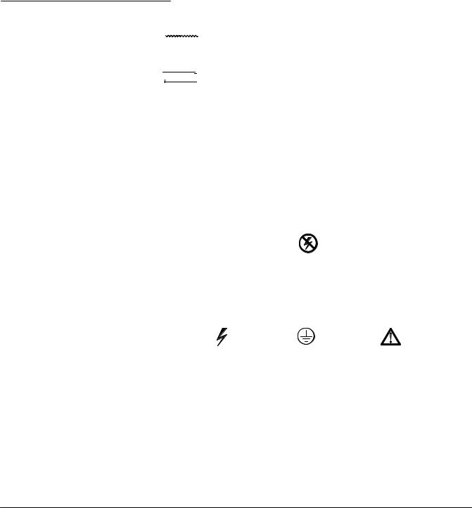
Symbols and Terms These two terms appear in manuals:
H statements identify conditions or practices that could result in damage to the equipment or other property
H
 statements identify conditions or practices that could result in personal injury or loss of life
These two terms appear on equipment:
HT indicates a personal injury hazard not immediately accessible as one reads the marking or a hazard to property including the equipment itself
HR indicates a personal injury hazard immediately accessible as one reads the marking
This symbol appears in manuals:
Static.Sensitive Devices
These symbols appear on equipment:
DANGER |
Protective |
ATTENTION |
High Voltage |
ground earth |
Refer to |
|
terminal |
manual |
TDS 310, TDS 320 & TDS 350 Service Manual |
x |

Safety Summary
Specific Precautions Observe all the following precautions to ensure your personal safety and to prevent damage to either the oscilloscope or equipment connected to it.
Do Not Perform Service While Alone
Do not perform internal service or adjustment of this product unless another person capable of rendering first aid and resuscitation is present.
Use Care When Servicing With Power On
Dangerous voltages exist at several points in this product. To avoid personal injury, do not touch exposed connections or components while power is on. Disconnect power before removing protective panels, soldering, or replacing components.
Power Source
The TDS 310, TDS 320, and TDS 350 operate from a power source that does not apply more than 250 VRMS between the supply conductors or between either supply conductor and ground. A protective ground connection, through the grounding conductor in the power cord, is essential for safe system operation.
Grounding the Oscilloscope
The oscilloscope is grounded through the power cord. To avoid electric shock, plug the power cord into a properly wired receptacle with an earth ground connection. Do this before making connections to the input or output terminals of the oscilloscope.
Without the protective ground connection, all parts of the oscilloscope are potential shock hazards. This includes knobs and controls that may appear to be insulators.
Use the Proper Power Cord
Use only the power cord and connector specified for your product. Use only a power cord that is in good condition.
Use the Proper Fuse
To avoid fire hazard, use only a fuse that meets all type, voltage, and current specifications on page 1-13.
Do Not Remove Covers or Panels
To avoid personal injury, do not operate the oscilloscope without the panels or covers.
x |
Section Name (Nm:Sect) |

Safety Summary
Do Not Operate in Explosive Atmospheres
The oscilloscope provides no explosion protection from static discharges or arcing components. Do not operate the oscilloscope in an atmosphere of explosive gasses.
Electric Overload
Never apply a voltage to a connector on the oscilloscope that is outside the range specified for that connector.
TDS 310, TDS 320 & TDS 350 Service Manual |
x |

Safety Summary
x |
Section Name (Nm:Sect) |

Specifications
This section contains complete specifications for the TDS 310, TDS 320, and TDS 350. The specifications are divided into three subsections, one for each of three classes of traits: warranted characteristics, typical characteristics, and nominal traits.
TDS 310, TDS 320 & TDS 350 Service Manual |
1 1 |

Specifications
1 2 |
Specifications |

Warranted Characteristics
Warranted characteristics are described in terms of quantifiable performance limits that are warranted. This subsection lists only warranted characteristics.
NOTE
Performance
Conditions
In these tables, those warranted characteristics that are checked in the Performance Tests, starting on page 4 11, appear in boldface type under the column Name.
The electrical characteristics found in these tables of warranted characteristics apply when the oscilloscope has been adjusted at an ambient temperature between +20_4C and +30_4C, has had a warm5up period of at least 20 minutes, and is operating at an ambient temperature between -10_4C and +55_4C (unless otherwise noted).
Table.101:/Warranted Characteristics 1 Signal Acquisition System
Name |
Description |
|
|
|
|
Accuracy, DC Voltage Measurement, |
Measurement Type |
DC Accuracy |
Average Acquisition Mode |
Average of ≥ 16 waveforms |
±(2.0% |(reading - |
|
||
|
|
Net Offset)| + Offset |
|
|
Accuracy + 0.1 div) |
|
Delta volts between any two av5 |
±(2.0% |reading| + 0.15 div |
|
erages of ≥ 16 waveforms ac5 |
+ 0.3 mV) |
|
quired under the same setup |
|
|
and ambient conditions |
|
|
|
|
Accuracy, DC Gain, Sample or |
±2% |
|
Average Acquisition Modes |
|
|
|
|
|
Pulse Response, Peak Detect and |
Sec/Div Setting |
Minimum Pulse Width |
Envelope Mode |
5 s/div - 25 s/div |
10 ns |
|
TDS 310:410 s/div - 10 ns/div TDS 320:410 s/div - 5 ns/div TDS 350:410 s/div - 2.5 ns/div
The greater of 10 ns or
.02 sec/div setting
TDS 310, TDS 320 & TDS 350 Service Manual |
1 3 |
Warranted Characteristics
Table5171:6Warranted Characteristics 8 Signal Acquisition System (Cont.)
Name |
Description |
|
|
|
|
Accuracy, Offset |
Volts/Div Setting |
Offset Accuracy |
|
2 mV/div - 99.5 mV/div |
±(0.4% |Net Offset1| |
|
|
+ 3 mV + 0.1 div V/div setC |
|
|
ting) |
|
100 mV/div - 995 mV/div |
±(0.4% |Net Offset1| |
|
|
+ 30 mV + 0.1 div V/div setC |
|
|
ting) |
|
1 V/div - 10 V/div |
±(0.4% |Net Offset1| |
|
|
+ 300 mV + 0.1 div V/div setC |
|
|
ting) |
|
|
|
Analog Bandwidth, DC Coupled |
TDS 310:ADC - ≥ 50 MHz |
|
|
TDS 320:ADC - ≥ 100 MHz |
|
|
TDS 350:ADC - ≥ 200 MHz; DC - ≥ 180 MHz for 2 mV/div |
|
|
|
|
Cross Talk (Channel Isolation) |
≥ 100:1 at 50 MHz with equal Volts/Div settings on each channel |
|
|
|
|
Input Impedance, DCCCoupled |
1 MW ±1% in parallel with 20 pF ±2.0 pF |
|
|
|
|
Input Voltage, Maximum |
±400 V (DC + peak AC); derate at 20 dB/decade above 100 kHz to |
|
|
13 V peak AC at 3 MHz and above |
|
|
|
|
Lower Frequency Limit, AC Coupled2 |
≤10 Hz |
|
1Net Offset = Offset - (Position × Volts/Div). Net offset is the voltage level at the center of the A7D converter dynamic range. Offset Accuracy is the accuracy of this voltage level.
2The AC Coupled Lower Frequency Limits are reduced by a factor of 10 when 10X, passive probes are used.
Table5172:6Warranted Characteristics 8 Time Base System
Name |
Description |
|
|
Accuracy, Long Term Sample Rate |
±100 ppm over any ≥ 1 ms interval |
and Delay Time |
|
|
|
Accuracy, Delta Time Measure7 |
For singleCshot acquisitions using sample acquisition mode and a |
ments1, 2 |
bandwidth limit setting of FULL: |
|
BB±(1 WI + 100 ppm |Reading| + 0.6 ns) |
|
For repetitive acquisitions using average acquisition mode with |
|
≥ 16 averages and a bandwidth limit setting of FULL: |
|
BB±(1 WI + 100 ppm |Reading| + 0.4 ns) |
|
|
1For input signals ≥ 5 divisions in amplitude and a slew rate of ≥ 2.0 divisions/ns at the delta time measurement points. Signal must be acquired at a volts/division setting ≥ 5 mV/division.
2The WI (waveform interval) is the time between the samples in the waveform record. Also, see the footnotes for Sample Rate Range and Equivalent Time or Interpolated Waveform Rates in Table 1711 on page 1712.
1 4 |
Specifications |

|
|
Warranted Characteristics |
|||
Table1133:2Warranted Characteristics 4 Triggering System |
|
|
|
||
|
|
|
|
|
|
Name |
Description |
|
|
|
|
|
|
|
|
|
|
Accuracy, Trigger Level, DC Coupled |
Trigger Source |
Sensitivity |
|
|
|
|
CH1 or CH2 |
±(3% of |Setting - Net Offset1| |
|||
|
|
+ 0.2 div volts/div setting + |
|
||
|
|
Offset Accuracy) |
|
|
|
|
External |
±(6% of |Setting| + 20 m |
) |
|
|
|
External/10 |
±(6% of |Setting| 200 m |
) |
|
|
|
|
|
|
|
|
Sensitivity, Edge3Type Trigger, DC |
Trigger Source |
Sensitivity |
|
|
|
Coupled |
CH1 or CH2 |
TDS 310: 0.35 division from DC |
|||
|
|||||
|
|
to 20 MHz, increasing to 1 div at |
|||
|
|
50 MHz |
|
|
|
|
|
TDS 320: 0.35 division from DC |
|||
|
|
to 50 MHz, increasing to 1 div at |
|||
|
|
100 MHz |
|
|
|
|
|
TDS 350: 0.35 division from DC |
|||
|
|
to 50 MHz, increasing to 1 div at |
|||
|
|
200 MHz |
|
|
|
|
External |
TDS 310: 50 m from DC to |
|
||
|
20 MHz, increasing to 150 m |
at |
|||
|
|
||||
|
|
50 MHz |
|
|
|
|
|
TDS 320: 50 m from DC to |
|
||
|
|
50 MHz, increasing to 150 m |
at |
||
|
|
100 MHz |
|
|
|
|
|
TDS 350: 50 m from DC to |
|
||
|
|
50 MHz, increasing to 150 m |
at |
||
|
|
200 MHz |
|
|
|
|
External/10 |
TDS 310: 500 m from DC to |
|
||
|
20 MHz, increasing to 1.5 |
at |
|
||
|
|
|
|||
|
|
50 MHz |
|
|
|
|
|
TDS 320: 500 m from DC to 50 |
|||
|
|
MHz, increasing to 1.5 |
at 100 |
||
|
|
MHz |
|
|
|
|
|
TDS 350: 500 m from DC to 50 |
|||
|
|
MHz, increasing to 1.5 |
at |
|
|
|
|
200 MHz |
|
|
|
|
|
|
|
|
|
Input Impedance, External Trigger |
1 MW ±2% in parallel with 20 pF ±2 pF |
|
|
|
|
|
|
||||
Maximum Input oltage, |
±400 (DC + peak AC); derate at 20 dB/decade above 100 kHz to |
||||
External Trigger |
13 peak AC at 3 MHz and above |
|
|
|
|
|
|
|
|
|
|
1Net Offset = Offset - (Position Volts/Div). Net Offset is the voltage level at the center of the A3D converter dynamic range. Offset Accuracy is the accuracy of this voltage level.
TDS 310, TDS 320 & TDS 350 Service Manual |
1 5 |

Warranted Characteristics
|
Table5174:6Power Requirements |
|
|
|
|
Name |
Description |
|
|
|
|
Source Voltage and Frequency |
90 to 132 VACRMS, continuous range, for 47 Hz through 440 Hz |
|
|
132 to 250 VACRMS, continuous range, for 47 Hz through 63 Hz |
|
Power Consumption |
≤65 Watts (120 VA) |
|
|
|
|
Table5175:6Warranted Characteristics 8 Environmental, Safety, and Reliability |
|
|
|
|
|
Name |
Description |
|
|
|
|
Atmospherics |
Temperature: |
|
|
-10_ C to +55_ C, operating; |
|
|
-51_ C to +71_ C, non@operating |
|
|
Relative humidity: |
|
|
to 95%, at or below +40_ C; to 75%, +41_ C to +55_ C |
|
|
Altitude: |
|
|
To 15,000 ft (4570 m), operating; |
|
|
to 40,000 ft (12190 m), non@operating |
|
|
|
|
Dynamics |
Random vibration: |
|
|
0.31 g RMS, from 5 to 500 Hz, 10 minutes each axis, operating; |
|
|
2.46 g RMS, from 5 to 500 Hz, 10 minutes each axis, |
|
|
non@operating |
|
|
|
|
Emissions1 |
Meets or exceeds the requirements of the following standards: |
|
|
EN 50081-1 European Community Requirements |
|
|
EN 55022 radiated emissions |
|
|
EN 55022 Class B conducted emissions |
|
|
EN 60555-2 power harmonics |
|
|
VFG 0243 |
|
|
FCC Rules and Regulations, 47 CFR, Part 15, Subpart B, Class A |
|
|
|
|
Susceptibility2 |
TDS 310 and TDS 320: ≤±0.2 division waveform displacement, or |
|
|
≤0.4 division increase in p@p noise. |
|
TDS 350: ≤±0.2 division waveform displacement, or ≤0.4 division increase in p@p noise below 200 MHz. ≤±0.3 division waveform dis@ placement, or ≤±0.6 division increase in p@p noise from 200 MHz to 500 MHz.
The instruments are subjected to the EMI specified in the following standards:
EN 50082-1 European Community Requirements
IEC 801-3 radiated susceptibility
IEC 801-4 fast transients
IEC 801-5 AC surge
1To maintain emission requirements when connecting to the I/O interface of this oscilloscope, use only a high7quality, double7shielded (braid and foil) cable. The cable shield must have low impedance connections to both connector housings. The VGA cable must also have ferrite cores at either end. Acceptable cables are listed in Table 776 on page 774.
2Susceptibility test run with both channel inputs terminated with grounding caps, both channels set to 2 mV/Div, DC Coupling, the trigger source set to Line, the Acquisition Mode set to Peak Detect, and the time base set to 25 s/Div.
1 6 |
Specifications |

Typical Characteristics
Typical characteristics are described in terms of typical or average |
||||
performance. Typical characteristics are not warranted. |
|
|||
Table5176:6Typical Characteristics 8 Signal Acquisition System |
|
|||
|
|
|
|
|
Name |
Description |
|
|
|
|
|
|
||
Accuracy, DC Gain, Envelope |
±3% for sec/div settings from 5 Sec/Div to 25 sec/div; |
|
||
Acquisition Mode |
TDS 310:?±2% for sec/div settings from 10 s/div to 10 ns/div; |
|||
|
TDS 320:?±2% for sec/div settings from 10 s/div to 5 ns/div; |
|||
|
TDS 350:?±2% for sec/div settings from 10 s/div to 2.5 ns/div |
|||
|
|
|
|
|
Accuracy, DC Voltage Measurement, |
Measurement Type |
|
DC Accuracy |
|
Sample Acquisition Mode |
Any Sample |
|
±(2.0% (|reading - Net |
|
|
|
|||
|
|
|
@Offset1|) + Offset Accuracy |
|
|
|
|
@+ 0.13 div + 0.6 mV) |
|
|
Delta Volts between any two samA |
±(2.0% |reading| + 0.26 div |
||
|
ples2 acquired under the same setA |
@+ 1.2 mV) |
|
|
|
up and ambient conditions |
|
|
|
|
|
|
|
|
Frequency Limit, Upper, 20 MHz |
20 MHz |
|
|
|
Bandwidth Limited |
|
|
|
|
|
|
|
|
|
Step Response Settling Error |
Volts/Div Setting |
Step |
Settling Error (%)3 |
|
|
|
Amplitude |
|
|
|
|
|
100 ns |
20 ms |
|
2 mV/div - 99.5 mV/div |
≤2 V |
≤1.0 |
≤0.1 |
|
100?mV/div> - |
≤20 V |
≤1.5 |
≤0.2 |
|
995 mV/div |
|
|
|
|
1 V/div - 10 V/div |
≤200 V |
≤2.5 |
≤0.2 |
|
|
|||
Common Mode Rejection Ratio |
100:1 at 60 Hz, reducing to 20:1 at 50 MHz, with equal Volts/Div and |
|||
(CMRR) |
Coupling settings on each channel. |
|
|
|
1Net Offset = Offset - (Position × Volts/Div). Net Offset is the voltage level at the center of the A7D converter dynamic range. Offset Accuracy is the accuracy of this voltage level.
2The samples must be acquired under the same setup and ambient conditions.
3The values given are the maximum absolute difference between the value at the end of a specified time interval after the mid7level crossing of the step, and the value one second after the mid7level crossing of the step, expressed as a percentage of the step amplitude.
TDS 310, TDS 320 & TDS 350 Service Manual |
1 7 |

Typical Characteristics
Table:1<7:;Typical Characteristics = Triggering System
Name |
Description |
|
|
|
|
Error, Trigger Position, Edge Triggering |
Acquire Mode |
Trigger<Position Error1,2 |
|
Sample, Average |
±(1 WI + 2 ns) |
|
Peak Detect, Envelope |
±(2 WI + 2 ns) |
|
|
|
Sensitivity, Video@Type Trigger |
Source |
Typical Sensitivity |
|
CH1 or CH2 |
0.6 division of video sync signal |
|
External |
75 mV of video sync signal |
|
External/10 |
750 mV of video sync signal |
|
|
|
Lowest Frequency for Successful Op@ |
50 Hz |
|
eration of •Set Level to 50%" Function |
|
|
|
|
|
Sensitivity, Edge Type Trigger, Not DC |
Trigger Coupling |
Typical Signal Level for Stable Trig< |
Coupled3 |
|
gering |
|
AC |
Same as DC@coupled limits4 for frequen@ |
|
|
cies above 60 Hz. Attenuates signals |
|
|
below 60 Hz. |
|
Noise Reject |
Three and one half times the DC@ |
|
|
coupled limits.4 |
|
High Frequency Reject |
One and one half times times the DC@ |
|
|
coupled limits4 from DC to 30 kHz. At@ |
|
|
tenuates signals above 30 kHz. |
|
Low Frequency Reject |
One and one half times the DC@coupled |
|
|
limits4 for frequencies above 80 kHz. |
|
|
Attenuates signals below 80?kHz. |
1The trigger position errors are typically less than the values given here. These values are for triggering signals having a slew rate at the trigger point of ±0.5 division/ns.
2The waveform interval (WI) is the time between the samples in the waveform record. Also, see the footnote for the characteristics
Sample Rate Range and Equivalent Time or Interpolated Waveform Rates in Table 1<11 on page 1<12.
3The minimum sensitivity for obtaining a stable trigger. A stable trigger results in a uniform, regular display triggered on the selected slope. The trigger point must not switch between opposite slopes on the waveform, and the display must not •roll" across the screen on successive acquisitions. The TRIG'D LED stays constantly lighted when the SEC/DIV setting is 2 ms or faster but may flash when the SEC/DIV setting is 10 ms or slower.
4See the characteristic Sensitivity, Edge Type Trigger, DC Coupled in Table 1<3, which begins on page 1<5.
Table:1<8:;Typical Characteristics = Probe Compensator Output
Name |
Description |
|
|
|
|
Output Voltage and Frequency, |
Characteristic |
|
Probe Compensator |
Voltage |
5.0 V (low@high) into a 1?MW load |
|
||
|
Frequency |
1 kHz |
|
|
|
1 8 |
Specifications |

Typical Characteristics
Table(1*9:)Typical Characteristics + Data Handling
Name |
Description |
|
|
Time, Data Retention, Nonvolatile |
≥ 5 Years |
Memory1,2 |
|
1The time that reference waveforms, stored setups, and calibration constants are retained when there is no power to the oscilloscope.
2Data is maintained by a lithium poly*carbon monofluoride battery.
TDS 310, TDS 320 & TDS 350 Service Manual |
1 9 |

Typic l Ch r ct ristics
1 10 |
Sp cific tions |

Nominal Traits
N/-*.", 42"*43 "2& %&3$2*#&% 53*.( 3*-0,& 34"4&-&.43 /' '"$4 35$) "3 •T7/, *%&.4*$"," '/2 4)& 42"*4 •I.054 C)"..&,3, N5-#&2 /'," 2"4)&2 4)". *. 4&2-3 /' ,*-*43 4)"4 "2& 0&2'/2-".$& 2&15*2&-&.43
Table91;10::Nominal Traits < Signal Acquisition System
Name |
Description |
|
|
|
|
B".%7*%4) S&,&$4*/.3 |
2 MHz ".% FULL |
|
|
|
|
D*(*4*z&23, N5-#&2 /' |
T7/, *%&.4*$",, %*(*4*z&% 3*-5,4".&/53,y |
|
|
|
|
D*(*4*z&% B*43, N5-#&2 /' |
8 #*431 |
|
I.054 C)"..&,3, N5-#&2 /' |
T7/, *%&.4*$",, $",,&% CH ".% CH 2 |
|
|
|
|
I.054 C/50,*.( |
DC, AC, /2 GND |
|
|
|
|
R".(&3, O''3&4, A,, C)"..&,3 |
Volts/Div Setting |
Offset Range |
|
2 -V %*6 - 99 -V %*6 |
± V |
|
-V %*6 - 99 -V %*6 |
± V |
|
V %*6 - V %*6 |
± V |
|
|
|
R".(&, P/3*4*/. |
± %*6*3*/.3 |
|
|
|
|
R".(&, S&.3*4*6*4y2 |
2 -V %*6 4/ V %*6 |
|
R*3& T*-& |
TDS 3 : .3 |
|
|
TDS 32 : 3 .3 |
|
|
TDS 3 : .3 |
|
|
|
|
T&+P2/#& I.4&2'"$& |
L&6&, /.& 02/#& $/%*.( |
|
|
|
|
1Displayed vertically with 25 digitization levels (DLs) per division and 10.24 divisions dynamic range with zoom off. A DL is the smallest voltage level change that the 8;bit A;D Converter can resolve, with the input scaled to the volts/division setting of the channel used. Expressed as a voltage, a DL is equal to 1/25 of a division times the volts/division setting.
2The sensitivity ranges from 2 mV/div to 10 V/div in a 1-2-5 sequence of coarse settings. Between consecutive coarse settings, the sensitivity can be finely adjusted with a resolution of 1% of the more sensitive setting. For example, between 50 mV/div and 1009mV/div, the volts/division can be set with 0.5 mV resolution.
TDS 310, TDS 320 & TDS 350 Service Manual |
1 11 |

Nominal Traits
Table,1.11:-Nominal Traits / Time Base System |
|
|
|
Name |
Description |
|
|
Range, Sample9Rate1,2 |
TDS 310: 10 Samples/s to 200 MSamples/s in a 1-2-5 sequence |
|
TDS 320: 10 Samples/s to 500 MSamples/s in a 1-2-5 sequence |
|
TDS 350: 10 Samples/s to 1 GSamples/s in a 1-2-5 sequence |
|
|
Range, Seconds/Division |
TDS 310: 10 ns/div to 5 s/div in a 1-2.5-5 sequence |
|
TDS 320: 5 ns/div to 5 s/div in a 1-2.5-5 sequence |
|
TDS 350: 2.5 ns/div to 5 s/div in a 1-2.5-5 sequence |
|
|
Range, Time Base Delay Time |
16.5 ns to 50 seconds |
|
|
Record Length |
1,000 samples |
|
|
1The range of real.time rates, expressed in samples/second, at which a digitizer samples signals at its inputs and stores the samples in memory to produce a record of time.sequential samples
2The Waveform Rate (WR) is the equivalent sample rate of a waveform record. For a waveform record acquired by real.time sampling of a single acquisition, the waveform rate is the same as the real.time sample rate; for a waveform created by interpolation of real.time samples from a single acquisition or by equivalent.time sampling of multiple acquisitions, the waveform rate is faster than the real time sample rate. For all three cases, the waveform rate is 1/(Waveform Interval) for the waveform record, where the waveform interval (WI) is the time between the samples in the waveform record.
Table,1.12:-Nominal Traits / Triggering System
Name |
Description |
|
|
|
|
Range, Hold Off |
500 ns minimum to 10 seconds maximum |
|
|
|
|
Ranges, Trigger Level |
Source |
Range |
|
Any Channel |
±12 divisions from center of screen |
|
External |
±1.5 Volts |
|
External /10 |
±15 Volts |
|
Line |
±300 Volts |
|
|
|
Formats and Field Rates, Video Trigger |
Triggers from sync9negative composite video, 525 to 625 lines, |
|
|
50 Hz to 60 Hz, interlaced or noninterlaced systems with scan rates |
|
|
from 15 kHz to 65 kHz - such as NTSC, PAL, or SECAM |
|
|
|
|
TekProbe Interface, External Trigger |
Level one probe coding |
|
|
|
|
1 12 |
Specifications |

|
Nominal Traits |
|
Table&1(13:'Nominal Traits ) Display System |
||
|
|
|
Name |
Description |
|
|
|
|
CRT Type |
7Binch 17.95 cm diagonal magnetic deflection; horizontal rasterB |
|
|
scan; P31 green phosphor |
|
|
|
|
Video Display Resolution |
640 pixels horizontally by 480 pixels vertically |
|
|
Display area is 5.04 inch 12.92 cm horizontally by 3.78 inch |
|
|
9.69 cm vertically |
|
|
|
|
Waveform Display Graticule |
A single graticule 401 501 pixels 8 10 divisions with divisions |
|
|
that are approximately 1 cm by 1 cm |
|
|
|
|
Intensity Levels |
Dim and Bright with adjustable Overall Intensity and Contrast |
|
|
|
|
Table&1(14:'Nominal Traits ) I/O Interface Option |
||
|
|
|
Name |
Description |
|
|
|
|
GPIB |
Part of Option 14 I/O interface or TD3F14A I/O interface field upB |
|
|
grade kit; complies with IEEE Std 488-1987 |
|
|
|
|
RSB232 |
Part of Option 14 I/O interface or TD3F14A I/O interface field upB |
|
|
grade kit; a 9Bpin male DTE RSB232 interface that complies with |
|
|
EIA/TIA 574-90 |
|
|
|
|
Centronics |
Part of Option 14 I/O interface or TD3F14A I/O interface field upB |
|
|
grade kit; a 25Bpin IBM PCBtype parallel printer interface that comB |
|
|
plies electrically with Centronics C332-44 Rev A |
|
|
|
|
Video Signal Output |
DBB9 rear panel Video connector; nonBinterlaced with levels that |
|
Option 14 Only TDS310 and |
comply with ANSI RS343A |
|
TDS 350 B020100 and above; |
VGA compatible at a 30.6 kHz sync rate |
|
TDS 320 B030100 and above |
||
|
||
|
|
|
Power Supply Printer |
Power supply connector to supply power to the Option 3P Printer |
|
Option 14 Only TDS310 and |
Pack |
|
TDS 350 B020100 and above; |
|
|
TDS 320 B030100 and above |
|
|
|
|
|
Table&1(15:'Nominal Traits ) Power Distribution System |
||
|
|
|
Name |
Description |
|
|
|
|
Fuse Rating |
5 mm × 20 mm UL 198 G : 3 A Slow 250 V IEC 127 : 3.15 A T |
|
|
250AV |
|
|
|
|
TDS 310, TDS 320 & TDS 350 Service Manual |
1 13 |
 Loading...