

Standard Microsystems Corporation FDC37N958FR Datasheet

FDC37N958FR
Notebook I/O Controller with Enhanced Keyboard
and System Control
FEATURES
- Asynchronous Access to Two Data
!
5 Volt Operation
!
ACPI 1.0 Compliant
!
PC 99 Compliant
!
Three Power Planes
!
<20"A Consumption in Sleep Mode
!
Configuration Register Set Compatible with
ISA Plug-and-Play Standard (Version 1.0a)
!
Serial IRQ meets IRQ Specification for PCI
Systems
- Quiet (Active) Mode
- Continuous (Idle) Mode
!
8051 Controller uses Parallel Port to
Reprogram the Flash ROM
!
IR Interface Fully Compliant to IrDA 1.1
(Fast IR)
- TEMIC/IBM Module Support
- HP Module Support
- Sharp Module Support
!
ISA Host Interface
- 16 Bit Address Qualification
- 8 Bit Data bus
- Zero Wait-State I/O Register Access
- All Write Only Registers are Shadowed
- IOCHRDY for ECP and Flash Cycles
- 8 Direct IRQs Including nSMI
- Four 8 Bit DMA Channels
!
System Flash Interface (256Kx8)
- 8051/Host CPU Multiplexed Interface
- Eight 32K pages - 8051 Keyboard BIOS
- Four 64K pages - Host System BIOS
!
8051 Keyboard and System Controller
- Provides System Power Management
- System Watch Dog Timer (W DT)
- 8042 Style Host Interface
Registers and One Status Register
- Supports Interrupt and Polling Access
- 2K Internal ROM, nEA Pin Select
- 32K Bank Switchable External Flash Rom
Interface
- 256 Bytes Data RAM
- Access to On-Chip Control Registers via
MOVX External Data Access Commands
- Access to RTC and CMOS Registers
- Up to 16x8 Keyboard Scan Matrix
- Two 16 Bit Timer/Counter
- Integrated TX/RX Serial Interface
- Six 8051 Interrupt Sources
- Sixteen 8 Bit, Host/8051 Mailbox
Registers
- 19 Maskable Hardware Wake-Up Events
Supported
- Fast GATEA20
- Fast CPU_RESET
- Multiple Clock Sources and Frequencies
- IDLE and SLEEP Modes
!
Real Time Clock
- MC146818 and DS1287 Compatible
- 256 Bytes of Battery Backed CMOS in
Two Banks of 128 Bytes
- 128 Bytes of CMOS RAM Lockable in
4x32 Byte Blocks
- 12 and 24 Hour Time Format
- Binary and BCD Format
-<1"A Standby Current (typ)
!
ACCESS.bus Interface
- 8584 Style Interface
!
PS/2 Ports
SMSC DS – FDC37N958FR Rev. 09/01/99

- Four Independent Hardware Driven Ports
!
General Purpose I/O
- 22 I/O Pins
- 12 Out Pins
- 8 In Pins
!
Two Pulse Width Modulators
- Independent Clock Rates
- 7 Bit Duty Cycle Granularity
!
Intelligent Auto Power Management
!
2.88MB Super I/O Floppy Disk Controller
- Relocatable to 480 Different Addresses
- 13 IRQ Options
- 4 DMA Options
- Open Drain / Push-Pull Configurable
Output Drivers
- Licensed CMOS 765B Floppy Disk
Controller
- Advanced Digital Data Separator
- Software and Register Compatible with
SMSC's Proprietary 82077AA Compatible
Core
- Sophisticated Power Control Circuitry
(PCC) Including Multiple Powerdown
Modes for Reduced Power Consumption
- Supports Two Floppy Drives Directly
- 24 mA AT Bus Drivers
- Low Power CMOS Design
!
Floppy Disk Interface on Parallel Port
!
Licensed CMOS 765B Floppy Disk Controller
Core
- Supports Vertical Recording Format
- 16 Byte Data FIFO
- 100% IBM® Compatibility
- Detects All Overrun and Underrun
Conditions
- 48 mA Drivers and Schmitt Trigger Inputs
- DMA Enable Logic
- Data Rate and Drive Control Registers
IBM, PC/XT and PC/AT are registered tradem arks and PS/2 is a trademark of International B usiness Machines Corporation.
SMSC is a registered trademark and Ultra I/O, ChiProtect, and Multi-Mode are trademarks of Standard Microsystems
Corporation
!
Enhanced Digital Data Separator
- Low Cost Implementation
- No Filter Components Required
- 2 Mbps, 1 Mbps, 500 Kbps, 300
Kbps, 250 Kbps Data Rates
- Programmable Precompensation Modes
!
Multi-Mode# Parallel Port with ChiProtect
- Relocatable to 480 Different Addresses
- 13 IRQ Options
- 4 DMA Options
- Enhanced Mode
- Standard Mode:
- IBM PC/XT®, PC/AT®, and PS/2
Compatible Bidirectional Parallel Port
- Enhanced Parallel Port (EPP)
Compatible
- EPP 1.7 and EPP 1.9 (IEEE 1284
Compliant)
- High Speed Mode
- Microsoft and Hewlett Packard
!
Serial Ports
Extended Capabilities Port (ECP)
Compatible (IEEE 1284 Compliant)
- Incorporates ChiProtect# Circuitry for
Protection Against Damage Due to
Printer Power-On
- 12 mA Output Drivers
- Relocatable to 480 Different Addresses
- 13 IRQ Options
- Two High Speed NS16C550A
Compatible UARTs with Send/Receive 16
Byte FIFOs
- Programmable Baud Rate Generator
- Modem Control Circuitry Including 230K
and 460K Baud
- IrDA, HP-SIR, ASK-IR Support
#
#
ORDERING INFORMATION
Order Number: FDC37N958FRTQFP
208 Pin QFP/TQFP Package Options
SMSC DS – FDC37N958FR Rev. 09/01/99

TABLE OF CONTENTS
GENERAL DESCRIPTION......................................................................................................................1
PIN CONFIGURATION............................................................................................................................ 2
DESCRIPTION OF PIN FUNCTIONS...................................................................................................... 3
ALTERNATE FUNCTION PIN LIST ...................................................................................................... 10
BUFFER TYPE DESCRIPTIONS .......................................................................................................... 12
FUNCTIONAL DESCRIPTION...............................................................................................................13
AUTO POWER MANAGEMENT............................................................................................................ 17
FLOPPY DISK CONTROLLER ............................................................................................................. 23
FDC INSTRUCTION SET ...................................................................................................................... 50
FDC DATA TRANSFER COMMANDS.................................................................................................. 62
FDC CONTROL COMMANDS............................................................................................................... 71
COMPATIBILITY................................................................................................................................... 77
SERIAL PORT (UART).......................................................................................................................... 80
REGISTER DESCRIPTION ................................................................................................................... 80
PROGRAMMABLE BAUD RATE GENERATOR..................................................................................89
FIFO INTERRUPT MODE OPERATION................................................................................................ 91
FIFO POLLED MODE OPERATION......................................................................................................91
NOTES ON SERIAL PORT FIFO MODE OPERATION ........................................................................ 96
INFRARED COMMUNICATIONS CONTROLLER (IRCC) .................................................................... 98
IRRX/IRTX PIN ENABLE....................................................................................................................... 99
IR REGISTERS - LOGICAL DEVICE 5 ............................................................................................... 100
IR DMA CHANNELS............................................................................................................................101
SMSC DS – FDC37N958FR Rev. 09/01/99

IR IRQS................................................................................................................................................ 101
PARALLEL PORT............................................................................................................................... 102
PARALLEL PORT INTERFACE MULTIPLEXOR............................................................................... 124
HOST (LEGACY) PARALLEL PORT INTERFACE (FDC37N958FR STANDARD)............................ 125
PARALLEL PORT FDC INTERFACE ................................................................................................. 125
PARALLEL PORT - 8051 CONTROL (FDC37N958FR STANDARD)................................................ 126
8051 EMBEDDED CONTROLLER...................................................................................................... 127
FEATURES.......................................................................................................................................... 127
8051 FUNCTIONAL OVERVIEW......................................................................................................... 127
8051 MEMORY MAP........................................................................................................................... 131
8051 CONTROL REGISTERS............................................................................................................. 136
WATCH DOG TIMER...........................................................................................................................151
SHARED FLASH INTERFACE............................................................................................................ 153
8051 SYSTEM POWER MANAGEMENT............................................................................................ 158
KEYBOARD CONTROLLER............................................................................................................... 168
MAILBOX REGISTER INTERFACE.................................................................................................... 181
PS/2 INTERFACE DESCRIPTION.......................................................................................................184
ACCESS.BUS INTERFACE DESCRIPTION....................................................................................... 185
LED CONTROLS................................................................................................................................. 189
PULSE WIDTH MODULATORS..........................................................................................................190
REAL TIME CLOCK CMOS ACCESS.................................................................................................190
8051 CONTROLLED PARALLEL PORT ............................................................................................ 193
8051 CONTROLLED IR PORT............................................................................................................ 196
SMSC DS – FDC37N958FR Rev. 09/01/99

GENERAL PURPOSE I/O (GPIO)....................................................................................................... 197
MULTIPLEXED PINS .......................................................................................................................... 203
REAL TIME CLOCK............................................................................................................................ 209
VCC1 POR........................................................................................................................................... 211
INTERNAL REGISTERS ..................................................................................................................... 212
TIME CALENDAR AND ALARM.........................................................................................................213
UPDATE CYCLE ................................................................................................................................. 214
CONTROL AND STATUS REGISTERS.............................................................................................. 215
INTERRUPTS...................................................................................................................................... 220
FREQUENCY DIVIDER.......................................................................................................................220
PERIODIC INTERRUPT SELECTION................................................................................................. 220
POWER MANAGEMENT.....................................................................................................................221
ACCESS.BUS...................................................................................................................................... 222
BACKGROUND................................................................................................................................... 222
REGISTER DESCRIPTION ................................................................................................................. 223
PS/2 DEVICE INTERFACE..................................................................................................................229
PS/2 LOGIC OVERVIEW..................................................................................................................... 229
SERIAL INTERRUPTS........................................................................................................................233
FDC37N958FR CONFIGURATION.....................................................................................................238
CONFIGURATION ELEMENTS...........................................................................................................238
TYPICAL SEQUENCE OF CONFIGURATION OPERATION.............................................................. 239
CONFIGURATION REGISTERS.........................................................................................................241
OPEN MODE REGISTERS..................................................................................................................266
SMSC DS – FDC37N958FR Rev. 09/01/99

ELECTRICAL SPECIFICATIONS........................................................................................................269
LOAD CAPACITANCE........................................................................................................................ 274
TIMING DIAGRAMS............................................................................................................................ 275
FUNCTIONAL REVISION ADDENDUM.............................................................................................. 308
FDC37N958FR ERRATA SHEET........................................................................................................309
SMSC DS – FDC37N958FR Rev. 09/01/99

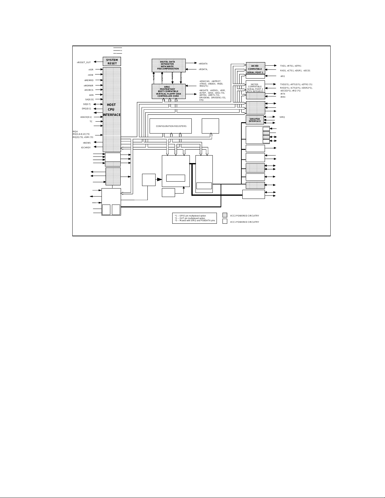
GENERAL DESCRIPTION
The FDC37N958FR is compliant with ACPI 1.0
and PC 97 and incorporates an 8051 based
keyboard controller; a Flash Interface; four PS/2
ports; real-time clock; SMSC's true CMOS 765B
FDC with advanced digital data separator and 16
byte data FIFO; two 16C550A compatible UARTs,
the second UART contains a Synchronous
Communications Engine to provide for IrDA Ver
1.1 (Fast IR) compliance; one Multi-Mode parallel
port which includes ChiProtect
TM
circuitry plus
EPP and ECP support; 8584 style Access Bus
interface; Serial IRQ peripheral agent interface;
General Purpose I/O; Two independent pulse
width modulators; on-chip 24 mA AT bus drivers
and two floppy direct drive support. The true
CMOS 765B core provides 100% compatibility
with IBM PC/XT and PC/AT architectures in
addition to providing data overflow and underflow
protection. The SMSC advanced digital data
separator incorporates SMSC's patented data
separator technology, allowing for ease of testing
and use. Both on-chip UARTs are compatible
with the NS16C550A. The parallel port is
compatible with IBM PC/AT architecture, as well
as EPP and ECP. The 8051 controller can also
take control of the parallel port interface to provide
remote diagnostics or “Flashing” of the Flash
memory. The FDC37N958FR has three
separate power planes which allows it to provide
“instant on” and system power management
functions. Additionally, the FDC37N958FR
incorporates sophisticated power control circuitry
(PCC). The PCC supports multiple low power
down modes.
The FDC37N958FR’s configuration register set is
compatible with the ISA Plug-and-Play Standard
(Version 1.0a) and provides the functionality to
support Windows '95. Through internal
configuration registers, each of the
FDC37N958FR's logical device's I/O address,
DMA channel and IRQ channel may be
programmed. There are 480 I/O address location
options, 13 IRQ options, and 4 DMA channel
options for each logical device.
The FDC37N958FR does not require any external
filter components and is, therefore, easy to use
and offers lower system cost and reduced board
area. The FDC37N958FR is software and
register compatible with SMSC's proprietary
82077AA core.
SMSC DS – FDC37N958FR Page 1 Rev. 09/01/99
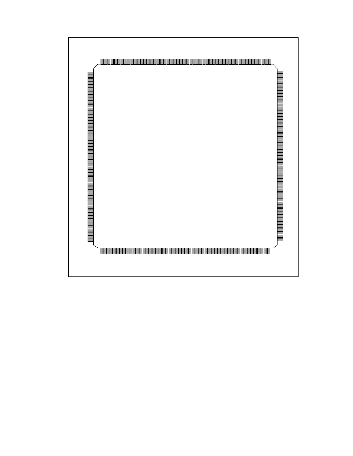
PIN CONFIGURATION
nRESET_OUT
GND
PWRGD
32KHz_OUT
PE
nPWR_LED
24MHz_OUT
nERROR
nSTB
GND
nDCD1
nDSR1
nCTS1
nRTS1
RXD1
TXD1
VCC0
IN5
IN6
IN7
GPIO12
IN0
IN1
IN2
IN3
IN4
GPIO8
GPIO9
VCC1
nRI1
nDTR1
GPIO15
GPIO14
GPIO13
GPIO10
GPIO11
PD0
nALF
nSLCTIN
nINIT
PD5
PD4
PD3
PD2
PD1
VCC2
SLCT
PD7
PD6
BUSY
nACK
VCC1_PWGD
XOSEL
XTAL1
XTAL2
AGND
FAD0
FAD1
FAD2
FAD3
FAD4
FAD5
GND
FAD6
FAD7
FA8
FA9
FA10
FA11
FA12
FA13
VCC1
FA14
FA15
FA16
FA17
FALE
nFRD
nFWR
GPIO0
GPIO1
GPIO2
GPIO3
GPIO4
GPIO5
GPIO6
GPIO7
GND
nEA
MODE
AB_DATA
AB_CLK
nBAT_LED
nFDD_LED
OUT11
OUT10
OUT9
OUT8
IRRX
IRTX
VCC2
GPIO17
GPIO18
GPIO19
155
150
151
152
153
154
156
157
158
159
160
161
162
163
164
165
166
167
168
169
170
171
172
173
174
175
176
177
178
179
180
181
182
183
184
185
186
187
208 PIN PQFP/TQFP
188
189
190
191
192
193
194
195
196
197
198
199
200
201
202
203
204
205
206
207
208
123456789101112131415161718192022232425262728293031323334353637383940414243444546474849505152
144
145
146
147
148
149
FDC37N958FR
138
139
140
141
142
143
132
133
134
135
136
137
21
126
127
128
129
130
131
120
121
122
123
124
125
114
115
116
117
118
119
108
109
110
111
112
113
105
106
107
104
VCC2
103
CLOCKI
102
OUT7
101
SIRQ
100
PSBDAT
99
PSBCLK
98
nMEMWR
97
nMEMRD
96
nROMCS
95
IOCHRDY
94
TC
93
DRQ1
92
nDACK1
91
DRQ0
90
nDACK0
89
GND
88
SD7
87
SD6
86
SD5
85
SD4
84
SD3
83
VCC2
82
SD2
81
SD1
80
SD0
79
AEN
78
nIOW
77
nIOR
76
nNOWS
75
OUT4
74
OUT3
73
GND
72
OUT2
71
OUT1
70
OUT0
69
SA15
68
SA14
67
SA13
66
SA12
65
SA11
64
SA10
63
SA9
62
SA8
61
SA7
60
SA6
59
SA5
58
SA4
57
SA3
56
SA2
55
SA1
54
SA0
53
GPIO21
IMCLK
IMDAT
KBCLK
KSI4
KSI3
KSI2
KSI1
KSI0
EMCLK
KSI7
KSI6
KSO8
KSO7
VCC2
KSO6
KSO5
KSO4
nINDEX
nWDATA
nTRK0
nRDATA
nWGATE
nWPROT
nDSKCHG
MID_0
KSO13
KSO12
KSO11
KSO10
GND
GND
nDS0
nSTEP
nHDSEL
nDIR
DRVDEN0
DRVDEN1
OUT5
OUT6
nMTR0
GPIO16
KSO9
FPD
KSO3
KSI5
KSO2
KSO1
KSO0
KBDAT
EMDAT
GND
GPIO20
FIGURE 1 - FDC37N958FR PIN CONFIGURATION
SMSC DS – FDC37N958FR Page 2 Rev. 09/01/99

DESCRIPTION OF PIN FUNCTIONS
SUPPLY
PinPin
PIN #
80:82,
84:88
54:69 SA[0:15] System Address Bus VCC2 I
96 nROMCS ROM Chip Select VCC2 I
79 AEN Address Enable (DMA master has
95 IOCHRDY I/O Channel Ready VCC2 OD24
91,93 DRQ[0:1] DMA Requests VCC2 O24
202, 201 DRQ[2:3]/
90, 92 nDACK[0:1] DMA Acknowledge VCC2 I
207, 208 nDACK[2:3]/
94 TC Terminal Count VCC2 I
77 nIOR I/O Read VCC2 I
78 nIOW I/O Write VCC2 I
97 nMEMRD Memory Read VCC2 I
98 nMEMWR Memory Write VCC2 I
70 IRQ6(FDC)/
71 nIRQ8/
72 IRQ7(PP)/
74 IRQ12(M)/
75 IRQ1(KB)/
76 nNOWS No Wait State VCC2 OD24
161:166,
168:169
170:175,
177:180
182 nFRD Flash Memory Read VCC1 O8
NAME DESCRIPTION
VOLTAGE TYPE
HOST (ISA) INTERFACE
SD[0:7] System Data Bus VCC2 I/O24
VCC2 I
bus control)
DMA Requests/GP Outputs VCC2 O24
OUT[8:9]
DMA Acknowledge/GPIO 18,19 VCC2 I/IO8
GPIO18, 19
OUT0
OUT1
OUT2
OUT3
OUT4
Floppy Disk Interrupt Request/
Generic Output 0
Active low Interrupt Request 8/
Generic Output 1
Parallel Port Interrupt Request/
Generic Output 2
Mouse Interrupt Request/
Generic Output 3
Keyboard Interrupt Request/
Generic Output 4
VCC2 O24
VCC2 O24
VCC2 O24
VCC2 O24
VCC2 O24
FLASH ROM/ MEMORY MAP INTERFACE
FAD[7:0] Flash Address/Data[7:0] Bus VCC1 I/O8
FA[8:17] Flash Address[17:8] VCC1 O8
SMSC DS – FDC37N958FR Page 3 Rev. 09/01/99
DESCRIPTION OF PIN FUNCTIONS
SUPPLY
PinPin
PIN #
183 nFWR Flash Memory Write VCC1 O8
181 FALE Flash Address latch Enable VCC1 O8
36:30,
28:22
44:37 KSI[0:7] Keyboard Scan Inputs VCC1 ISP
193 nEA External Access for 2K ROM VCC1 I
45 EMCLK EM Serial Clock VCC2
46 EMDAT EM Se rial Data VCC2
47 IMCLK IM Serial Clk VCC2
48 IMDAT IM Serial Data VCC2
50 KBCLK KBD Serial Clock VCC2
51 KBDAT KBD Serial Data VCC2
52 PS2CLK/
53 PS2DAT/
101 SIRQ /
99 PSBCLK PCI Clock input VCC2 I
100 PSBDAT UART2 Interrupt VCC2 I/O24
The following FDC output pins can be configured as either Open Drain outputs capable of
sinking 24mA (OD24) or as push-pull outputs capable of driving 12mA and sinking 24mA (O24).
The FDC output pins must tristate when the FDC is in powerdown mode (The board designer
must provide external pull-up resistors on these output pins).
17 nRDATA Read Disk Data VCC2 IS
12 nWGATE Write Gate VCC2 O24/
11 nWDATA Write Disk Data VCC2 O24/
NAME DESCRIPTION
KEYBOARD
KSO[0:13] Keyboard Scan Outputs(14*8 = 112)
Configuring GPIO4 and GPIO5 as
KSO14 and KSO15 yields a scan
matrix of 16 x 8 = 128.
PS2 Serial Clock VCC2
8051RX/
GPIO[20]
PS2 Serial Data VCC2
8051TX/
GPIO[21]
SERIAL IRQ / UART IRQS
Serial Interrupt
IRQ3(UA1)
UART1 Interrupt
FDD INTERFACE
VOLTAGE TYPE
VCC1 OD4
I/OD 24
I/OD 24
I/OD 24
I/OD 24
I/OD 24
I/OD 24
I/OD24
I/OD24
VCC2 I/O24
/O24
/O24
OD24
OD24
SMSC DS – FDC37N958FR Page 4 Rev. 09/01/99

DESCRIPTION OF PIN FUNCTIONS
SUPPLY
PinPin
PIN #
13 nHDSEL Head Select (1 = side 0 ) VCC2 O24/
9 nDIR Step Direction (1 = out ) VCC2 O24/
10 nSTEP Step Pulse VCC2 O24/
18 nDSKCHG Disk Change VCC2 IS
8 nDS0 Drive Select 0 VCC2 O24 /
6 nMTR0 Motor On 0 VCC2 O24 /
2nDS1/
3nMTR1/
16 nWPROT Write Protected VCC2 IS
15 nTRK0 Track 0 VCC2 IS
14 nINDEX Index Pulse Input VCC2 IS
4:5 DRVDEN[0:1] Drive Density Select [0:1] VCC2 O24 /
19 MID[0] Media ID 0 input. In floppy
20 MID[1]/
21 FPD Floppy Power Down output control.
130 RXD1 Receive Serial Data 1 VCC2 I
131 TXD1 Transmit Serial Data 1 VCC2 O4
134 nRTS1 Request to Send 1 VCC2 O4
135 nCTS1 Clear to Send 1 VCC2 I
136 nDTR1 Data Terminal Ready 1 VCC2 O4
NAME DESCRIPTION
Drive Select 1/
OUT5
Output 5
Motor On 1/
OUT6
Output 6
enhanced mode 2 this input is the
media ID [0] input.
Media ID 1 input. In floppy
GPIO16
enhanced mode 2 this input is the
media ID [1] input.
General Purpose I/O
This is the output of three power
down modes of the floppy (3F4,
auto-power down, configuration).
SERIAL PORT 1 INTERFACE
VOLTAGE TYPE
OD24
OD24
OD24
OD24
OD24
VCC2 O24 /
OD24/
VCC2 O24 /
OD24
OD24
VCC2 IS
VCC2 IS
VCC2 O8
O24
O24
I/O8
SMSC DS – FDC37N958FR Page 5 Rev. 09/01/99

DESCRIPTION OF PIN FUNCTIONS
SUPPLY
PinPin
PIN #
133 nDSR1 Data Set Ready 1 VCC2 I
137 nDCD1 Data Carrier Detect 1 VCC2 I
138 nRI1 Ring Indicator 1 VCC1 I
141 RXD2/
142 TXD2/
145 nRTS2/
146 nCTS2/
147 nDTR2/
144 nDSR2/
140 nDCD2/
139 nRI2 /
124:121,
119:116
125 nSLCTIN Printer Select VCC2 OD24/
126 nINIT Initiate Output VCC2 OD24/
128 nALF Auto Line Feed VCC2 OD24/
129 nSTB Strobe Signal VCC2 OD24/
114 BUSY Busy Signal VCC2 I
115 nACK Acknowledge Handshake VCC2 I
113 PE Paper End VCC2 I
112 SLCT Printer Selected VCC2 I
127 nERROR Error at Printer VCC2 I
NAME DESCRIPTION
VOLTAGE TYPE
SERIAL PORT 2 INTERFACE
GPIO8
GPIO9
GPIO10
GPIO11
GPIO12
GPIO13
GPIO14
GPIO15
Receive Serial Data 2/
General Purpose I/O 8
Transmit Serial Data 2/
General Purpose I/O 9
Request to Send 2/
General Purpose I/O 10
Clear to Send 2/
General Purpose I/O 11
Data Terminal Ready 2/
General Purpose I/O 12
Data Set Ready 2/
General Purpose I/O 13
Data Carrier Detect 2/
General Purpose I/O 14
Ring Indicator 2/
General Purpose I/O 15
VCC1 I /
VCC1 O8/
VCC1 O8/
VCC1 I/
VCC1 O8/
VCC1 I/
VCC1 I/
VCC1 I /
PARALLEL PORT INTERFACE
PD[0:7] Parallel Port Data Bus VCC2 I/O24
RTC
I/O8
I/O8
I/O8
I/O8
I/O8
I/O8
I/O8
I/O8
O24
O24
O24
O24
SMSC DS – FDC37N958FR Page 6 Rev. 09/01/99

DESCRIPTION OF PIN FUNCTIONS
SUPPLY
PinPin
PIN #
158 XTAL1 32 KHz Crystal Input VCC0 ICLK2
159 XTAL2 32 KHz Crystal Output VCC0
102 nSMI/
108 32 KHz_OUT 32 KHz Out -- The 32 KHz output is
109 24 MHz_OUT Programmable Clock Output.
103 CLOCKI 14.318 MHz Clock Input VCC2 ICLK
195 AB_DATA ACCESS.bus Serial Data VCC1 I/OD8
196 AB_CLK ACCESS.bus Clock VCC1 I/OD8
194 MODE Set Configuration register address VCC1 I
157 XOSEL Test Mode Enable Input Pin.
203 IRRX Infared Receive VCC2 I
204 IRTX Infared Transmit VCC2 O8
200 PWM0/
199 PWM1/
NAME DESCRIPTION
MISCELLANEOUS
System Management Interrupt/
OUT7
Output 7
enabled / disabled by setting /
clearing bit-0 of the Output Enable
8051 memory mapped register.
When disabled the 32 KHz_OUT pin
is driven low. The 32 KHz_OUT pin
defaults to the disabled state on
VCC1 POR.
1.8432 MHz (default = 24 MHz/13)
14.318 MHz
16 MHz
24 MHz
48 MHz
XOSEL = 1 is required to qualify all
pin defined test modes.
XOSEL = 0 prevents the pin test
modes from ever being invoked.
Pulse Width Modulator 0/
OUT10
Output 10
Pulse Width Modulator 1/
OUT11
Output 11
VOLTAGE TYPE
OCLK2
VCC2 O24
VCC1 O8
VCC2 O24
VCC1 I
VCC2 O24
VCC2 O24
SMSC DS – FDC37N958FR Page 7 Rev. 09/01/99

DESCRIPTION OF PIN FUNCTIONS
SUPPLY
PinPin
PIN #
105 VCC1_PWGD VCC1 Power Good Input pin. The
106 nRESET_OUT System reset (active low) VCC2 O8
197 nBAT_LED Battery LED (0=on) VCC1 OD24
110 nPWR_LED Power LED (0=on) VCC1 OD24
198 nFDD_LED Floppy LED. This pin is asserted
111 PWRGD Powergood VCC2 I
148 WK_EE4/IN0 Wakeup event/Generic Input 0 VCC1 I
149 WK_EE2/IN1 Wakeup event/Generic Input 1 VCC1 I
150 WK_EE3/IN2 Wakeup event/Generic Input 2 VCC1 I
151 nGPWKUP/
152 WK_HL1/IN4 Wakeup event/Generic Input 4 VCC1 I
153 WK_HL2/IN5 Wakeup event/Generic Input 5 VCC1 I
154 WK_HL6/IN6 Wakeup event/Generic Input 6 VCC1 I
155 WK_EE1/IN7 Wakeup event/Generic Input 7 VCC1 I
184 WK_HL3/
185 WK_HL4/
186 WK_HL5/
187 TRIGGER/
NAME DESCRIPTION
trailing edge of VCC1 POR is
released 20ms from the assertion of
this pin. If this pin is pulled low
while VCC1 is valid, then VCC1
POR will be asserted and held until
20ms from re-assertion of this pin.
This pin has an internal weak
(90"A) pull-up to VCC1.
whenever either DRVSEL1 or
DRVSEL0 is asserted or controlled
by the 8051. (0 = on)
Wakeup event/Generic Input 3 VCC1 I
IN3
Wakeup event/
GPIO0
GP I/O 0
Wakeup event/
GPIO1
GP I/O 1
Wakeup event/
GPIO2
GP I/O 2
Interrupt 1 event/
GPIO3
GP I/O 3
VOLTAGE TYPE
VCC1 I
VCC1 OD24
VCC1 I /
I/O8
VCC1 I /
I/O8
VCC1 I /
I/O8
VCC1 I/
I/O8
SMSC DS – FDC37N958FR Page 8 Rev. 09/01/99

Note:
Table 1
Power Pin List
-
Bias Pins
156 VCC0 RTC Supply Voltage
143,176 VCC1 8051 + AB +4.7V Supply Voltage (Note)
29,83,104,
VCC2 Core +5V Supply Voltage
120,205
160 AGND Analog Ground for VCC0.
1, 7, 49, 73, 89,
GND Ground
107, 132, 167, 192
AB = ACCESS.bus
SMSC DS – FDC37N958FR Page 9 Rev. 09/01/99
ALTERNATE FUNCTION PIN LIST
Table 2
Function I/O Type
Pin
Number
70 OUT0 IRQ6 (FDC) O24 O24 MISC0 VCC2
71 OUT1 nIRQ8 O24 O24
72 OUT2 IRQ7 (PP) O24 O24
74 OUT3 IRQ12(Mouse) O24 O24
75 OUT4 IRQ1(KBD) O24 O24
2OUT5 nDS1 O24 O24/OD24 MISC5
3OUT6 nMTR1 O24 O24/OD24
102 OUT7 nSMI O24 O24 MISC0
202 OUT8 DRQ2 (note1) |
201 OUT9 DRQ3 (note1) O24 O24 MISC11
200 OUT10 PWM0 O24 O24 MISC4
199 OUT11 PWM1 O24 O24
148 IN0 WK_EE4 I I alternate VCC1
149 IN1 WK_EE2 I I input masked
150 IN2 WK_EE3 I I by wake-up mask
151 IN3 nGPWKUP I I
152 IN4 WK_HL1 I I
153 IN5 WK_HL2 I I
154 IN6 WK_HL6 I I
155 IN7 WK_EE1 I I
184 GPIO0 WK_HL3 I/O8 I VCC1
185 GPIO1 WK_HL4 I/O8 I
Default Alternate Default Alternate
CPU_RESET
Alternate Function Pin List
-
O24
O24 MISC10 + MISC6
Mux
Control
Register bits
VCC
Plane
186 GPIO2 WK_HL5 I/O8 I
187 GPIO3 TRIGGER I/O8 I Masked by INT1
188 GPIO4 KSO14 I/O8 OD8 MISC9
189 GPIO5 KSO15 I/O8 OD8
190 GPIO6 IR_MODE | FRX I/O8 O8 | I MISC[14:13]
191 GPIO7 I/O8
141 GPIO8 COM-RX I/O8 IMISC7
142 GPIO9 COM-TX I/O8 O8 (note2)
145 GPIO10 nRTS2 |
IR_MODE | FRX
146 GPIO11 nCTS2 I/O8 IMISC12
147 GPIO12 nDTR2 I/O8 O8 (note2)
144 GPIO13 nDSR2 I/O8 I
140 GPIO14 nDCD2 I/O8 I
SMSC DS – FDC37N958FR Page 10 Rev. 09/01/99
I/O8
O8 | O8 | I
(note1)
mask register bit
3
MISC[16:15]
Function I/O Type
Pin
Number
139 GPIO15 nRI2 I/O8 I
20 GPIO16 MID1 IS/O8 IS MISC8 VCC2
206 GPIO17 GATEA20 I/O8 O8 MISC6
207 GPIO18 nDACK2 (note1) I/O8 IMISC17
208 GPIO19 nDACK3 (note1) I/O8 IMISC11
52 GPIO20 PS2CLK |
53 GPIO21 PS2DAT |
101 SIRQ IRQ3 (UA1) O8 O8 MISC0
23 KSO12 OUT8 OD4 OD4 MISC17 + 6 VCC1
22 KSO13 GPIO18 OD4 OD4 MISC17
Default
Alternate Default Alternate
8051RX
I/OD24
I/OD24
8051TX
I/OD24 | I MISC1 +
I/OD24 |
OD24
Mux
Control
MISC3
VCC
Plane
Note 1:
Note 2:
With the inclusion of Fast IR two additional DMA channels are provided.
W hen GPIO6, GPIO9, GPIO10 and/or GPIO12 are configured as IR_MODE, COM-
TX, nRTS2|IR_MODE, and/or nDTR2 respectively and POWERGOOD=0 (VCC2 low)
then these pins will tri-state to prevent back-biasing of external circuitry.
The Mux Control Column in Table 2 lists the Misc Bits which the 8051 has access to through the three
Multiplexing registers. See the 8051 section of this data sheet for a description of the Multiplexing
registers.
SMSC DS – FDC37N958FR Page 11 Rev. 09/01/99

BUFFER TYPE DESCRIPTIONS
I Input, TTL compatible.
IS Input with Schmitt trigger
ISP Input with Schmitt trigger, 90uA pull-up.
ICLK Input to crystal oscillator circuit (CMOS levels)
ICLK2 Crystal input
OCLK2 Output to external crystal
O4 Output, 4mA sink, 2mA source.
O8 Output, 8mA sink, 4mA source.
OD8 Open Drain Output, 8mA sink.
O8SR Output, 8mA sink, 4mA source with Slew Rate Limiting
O16 Output, 16mA sink, 8mA source.
OD16 Open Drain Output, 16mA sink.
O24 Output, 24mA sink, 12mA source.
OD24 Open Drain Output, 24mA sink.
OD48 Open Drain Output, 48mA sink
SMSC DS – FDC37N958FR Page 12 Rev. 09/01/99
nRESET_OUT
nIOR
nIOW
nMEMRD
nMEMWR
nROMCS
SA[0:15]
SD[0:7]
DRQ[0:1]
DRQ[2:3]*2
nDACK[0:1]
nDACK[2:3] *1
IRQ4
IRQ[1,6-8,12] (*2)
IRQ[3] (*3), nSMI (*2)
nNOWS
IOCHRDY
MODE
nEA
VCC1_PWGD
PWRGOOD
32KHz_OUT
24MHz_OUT
CLOCKI
(14.318 MHz)
XOSEL
XTAL2
XTAL1
VCC0
AGND
VCC1 (2)
VCC2 (5)
GND (9)
SYSTEM
RESET
AEN
HOST
CPU
INTERFACE
TC
CONTROL
ADDRESS
DATA
CONTROL
INPUTS
PLL CLOCK
GENERATOR
RTC
two 128B banks
of CMOS RAM
BANK
BANK
2
1
FUNCTIONAL DESCRIPTION
DIGITAL DATA
SEPARATOR
WITH WRITE
PRECOMPEN SATION
WCLOCK
RDATA
WDATA
SMSC
PROPRIETARY
82077 COMPA T IBLE
VERTICAL FLO PPY DISK
CONTROLLER CORE
CONTROL
ADDRESS
DATA
CONFIGURATION REGISTERS
8051
WDT
256B Direct RAM
Ring
Oscillator
*1 -- GPIO pin multiplexed option
*2 -- OUT p in multiplex ed option
*3 -- Muxe d with SIRQ and PSBDA TA pins
nWDATA
nRDATA,
RCLOCK
nDSKCHG, nWPROT,
nTRK0, nINDEX, MID0,
MID1(*1)
nWGATE, nHDSEL, nDIR,
nSTEP, nDS0, nDS1 (*2),
nMTR0, nMRT1 (*2),
DRVDEN0, DRVDEN1 (*2),
FPD
CONTROL
ADDRESS
DATA
POWER
MANAGEMENT
CONTROL
ADDRESS
DATA
MAILBOX
REGISTERS
8051
SUB-BLOCK
EXTERNAL
CONTROL
REGISTERS
256B Externa l
8051 RAM
16C550
COMPATIBLE
SERIAL POR T 1
16C550
COMPATIBL E
SERIAL PORT 2
WITH INFRARED
MULTI-MODE
PARALLEL
PORT / FDC MUX
SIRQ/PSB
INTERFACE
GENERAL
PURPOSE I/O
INTERFACE
LED DRIVER
16 x 8 MATRIX
KEYBOARD
INTERFACE
PS/2 PORTS
ACCESS BUS
PWM
28F020 (2Mb it)
FLASH INTERFACE
VCC2 POWERED CIRCUITRY
VCC1 POWERED CIRCUITRY
TXD1, nRTS1, nDTR1
RXD1, nCTS1, nDSR1, nDCD1
nRI1
TXD2(*1), nRTS2(*1), nDTR2 (*1)
RXD2(*1), nCTS2(*1), nDSR2(*1),
nDCD2(*1), nRI2 (*1)
IRTX
IRRX
PD[0:7]
BUSY, SLCT, PE, nERROR, nACK
nSTB, nSLCTIN, nIN IT , nALF
SIRQ
PSBCLK
PSBDAT
IN
IN0 - 7
OUT0 - 11
OUT
GPIO16 - 21
I/O
GPIO0 - 15
I/O
nBAT_LED, nPWR_LED, nFDD_LED
KSI[0:7]
KS0[0:13] , KS0[14:15](*2)
EMCLK, EMDAT, IMCLK, IMDAT
KBCLK, KBDAT, PS2CLK(* 1), PS2DAT( *1)
AB_DATA, AB_CLK
PWM0 (*2), PWM 1 (*2)
FAD[0: 7]
FA[8:17], nFRD, nFWR, FALE
FIGURE 2 - FUNCTIONAL BLOCK DIAGRAM
SMSC DS – FDC37N958FR Page 13 Rev. 09/01/99

FDC37N958FR OPERATING REGISTERS
HOST PROCESSOR INTERFACE
The address map, shown below in Table 3,
shows the set of operating registers and
addresses for each of the logical blocks of the
FDC37N958FR Ultra I/O controller. The base
addresses of the FDC, Parallel, Serial 1 and
Serial 2 ports can be moved via the configuration
registers.
Table 3 - FDC37N958FR Operating Register Addresses
LOGICAL
DEVICE
NUMBER
LOGICAL
DEVICE
BASE I/O
RANGE
(NOTE3)
0x00 FDC [0x100:0x0FF8]
ON 8 BYTE
BOUNDARIES
0x03 Parallel
Port
[0x100:0x0FFC]
ON 4 BYTE
BOUNDARIES
(EPP Not
supported)
or
[0x100:0x0FF8]
ON 8 BYTE
BOUNDARIES
(all modes
supported,
EPP is only
available when
the base
address is on an
8-byte boundary)
The host processor communicates with the
FDC37N958FR through a series of read/write
registers. The range of base I/O port addresses
for these registers is shown in Table 3. Register
access is accomplished through programmed I/O
or DMA transfers. All registers are 8 bits. Most of
the registers support zero wait-state access
(NOWS). All host interface output buffers are
capable of sinking a minimum of 12 mA.
ISA
FIXED
BASE OFFSETS
+0 : SRA
CYCLE
TYPE
NOWS
+1 : SRB
+2 : DOR
+3 : TSR
+4 : MSR/DSR
+5 : FIFO
+7 : DIR/CCR
+0 : Data / ecpAfifo
Std. ISA I/O
+1 : Status
+2 : Control
+400h : cfifo / ecpDfifo
tfifo / cnfgA
+401h : cnfgB
+402h : ecr
SMSC DS – FDC37N958FR Page 14 Rev. 09/01/99

LOGICAL
DEVICE
LOGICAL
NUMBER
0x04 Serial
DEVICE
BASE I/O
RANGE
(NOTE3)
[0x100:0x0FF8]
Port 1
ON 8 BYTE
BOUNDARIES
0x05 Serial Port2[0x100:0x0FF8]
ON 8 BYTE
BOUNDARIES
0x62,
0x63
[0x100:0x0FF8]
ON 8 BYTE
BOUNDARIES
0x06 RTC Not Relocatable
Fixed Base
Address
FIXED
BASE OFFSETS
+0 : RB/TB $ LSB div
+1 : IER % MSB div
+2 : IIR/FCR
+3 : LCR
+4 : MCR
+5 : LSR
+6 : MSR
+7 : SCR
+0 : RB/TB $ LSB div
+1 : IER % MSB div
+2 : IIR/FCR
+3 : LCR
+4 : MCR
+5 : LSR
+6 : MSR
+7 : SCR
+0 : Register Block N, address 0
+1 : Register Block N, address 1
+2 : Register Block N, address 2
+3 : Register Block N, address 3
+4 : Register Block N, address 4
+5 : Register Block N, address 5
+6 : Register Block N, address 6
+7 : USRT Master Control Reg.
0x70, 0x74 : Address Register
0x71, 0x76 : Data Register
ISA
CYCLE
TYPE
NOWS
NOWS
NOWS
Std. ISA I/O
SMSC DS – FDC37N958FR Page 15 Rev. 09/01/99

LOGICAL
DEVICE
NUMBER
LOGICAL
DEVICE
BASE I/O
RANGE
(NOTE3)
0x07 KYBD Not Relocatable
Fixed Base
Address
FIXED
BASE OFFSETS
0x60 : Data Register
0x64 : Command/Status Reg.
ISA
CYCLE
TYPE
NOWS
Note 1:
Note 2:
Note 3:
Refer to the configuration register descriptions for setting the base address
Serial Port 2 supports Infrared.
This chip uses all ISA address bits to decode the base address of each of its logical devices.
SMSC DS – FDC37N958FR Page 16 Rev. 09/01/99

AUTO POWER MANAGEMENT
Auto Power Management (APM) capabilities are
provided for the following logical devices: Floppy
Disk, UART 1, UART 2 and the Parallel Port. For
each logical device, two types of power
management are provided; direct powerdown and
auto powerdown.
System Power Management
See the “8051 System Power Management”
section for details.
FDC Power Management
Direct power management is controlled through
Global Configuration Register 22 (CR22). Refer
to CR22 in the Configuration section for more
information.
Auto Power Management is enabled through bit-0
of CR23. When set, this bit allows the FDC to
enter powerdown when all of the following
conditions have been met:
1. The motor enable pins of the FDC’s DOR
register are inactive (zero).
2. The FDC37N958FR must be idle; the MSR
register = 80h and the FDC’s INTerrupt = 0
(INT may be high even if MSR = 80H due to
polling interrupts).
3. The head unload timer must have expired.
4. The Auto powerdown timer (10msec) must
have timed out.
An internal timer is initiated as soon as the auto
powerdown command is enabled. The
FDC37N958FR is then powered down when all
the conditions are met.
Disabling the auto powerdown mode cancels the
timer and holds the FDC block out of auto
powerdown.
DSR From Powerdown
Bit 6 of the FDC’s DSR register is another FDC
powerdown bit. If DSR powerdown is used when
the FDC37N958FR is in auto powerdown, the
DSR powerdown will override the auto
powerdown. However, when the FDC37N958FR
is awakened from DSR powerdown, the auto
powerdown will once again become effective.
Wake Up From Auto Powerdown
If the FDC37N958FR enters the powerdown state
through the auto powerdown mode, then the
FDC37N958FR can be awakened by reset or by
appropriate access to certain registers.
If a hardware or software reset is used then the
FDC37N958FR will go through the normal reset
sequence. If the access is through the selected
registers, then the FDC resumes operation as
though it was never in powerdown. Besides
activating the RESET pin or one of the software
reset bits in the DOR or DSR registers, the
following register accesses will wake up the
FDC37N958FR:
1. Enabling any one of the motor enable bits in
the DOR register (reading the DOR does not
awaken the FDC37N958FR).
2. A read from the MSR register.
3. A read or write to the Data register.
Once awake, the FDC will reinitiate the auto
powerdown timer for 10 ms. The
FDC37N958FR will powerdown again when all
the powerdown conditions are satisfied.
SMSC DS – FDC37N958FR Page 17 Rev. 09/01/99

Register Behavior
Table 4 shows the AT and PS/2 (including Model
30) configuration registers available. It also shows
the type of access permitted. In order to maintain
software transparency, access to all the registers
is maintained. As Table 4 shows, two sets of
registers are distinguished based on whether their
access results in the FDC37N958FR remaining in
powerdown state or exiting it.
Access to all other registers is possible without
awakening the FDC37N958FR. These registers
can be accessed during powerdown without
changing the status of the FDC37N958FR. A
read from these registers will reflect the true
status as shown in the register description in the
FDC section. Writes to these registers will result
in the FDC37N958FR retaining the data and
subsequently reflecting it when the
FDC37N958FR awakens. Accessing the
FDC37N958FR during powerdown may cause an
increase in the power consumption by the
FDC37N958FR. The FDC37N958FR will revert
back to its low power mode when the access has
been completed.
Pin Behavior
The FDC37N958FR is specifically designed for
portable PC systems in which power conservation
is a primary concern. This makes the behavior of
the pins during powerdown very important.
The pins which interface to the floppy disk drive
are disabled so that no power will be drawn
through the FDC37N958FR as a result of any
voltage applied to the pin within the VCC2 power
supply range. Most of the pins which interface to
the system are left active to monitor system
accesses that may wake up the FDC37N958FR.
SMSC DS – FDC37N958FR Page 18 Rev. 09/01/99
System Interface Pins
Table 5 gives the state of the system interface
pins in the powerdown state. Pins unaffected by
Table 4 - PC/AT and PS/2 Available Registers
the powerdown are labeled "Unchanged". Input
pins are "Disabled" to prevent them from causing
currents internal to the FDC37N958FR when they
have indeterminate input values.
Note 1:
BASE + ADDRESS
AVAILABLE REGISTERS ACCESS
PERMITTED
PC/AT PS/2 (Model 30)
Access to these registers DOES NOT wake up the FDC37N 958FR
00H ---- SRA R
01H ---- SRB R
02H DOR (1) DOR (1) R/W
03H --- --- --04H DSR (1) DSR (1) W
06H --- --- --07H DIR DIR R
07H CCR CCR W
Access to these registers wakes up the FDC37N958FR
04H MSR MSR R
05H Data Data R/W
Writing to the DOR or DSR does not wake up the FDC37N958FR, however, writing any of the
motor enable bits or doing a software reset (via DOR or DSR reset bits) will wake up the
FDC37N958FR.
SMSC DS – FDC37N958FR Page 19 Rev. 09/01/99

Table 5 - State of System Pins in FDC Auto Powerdown
SYSTEM PINS STATE IN AUTO POWERDOWN
Input Pins
nIOR Unchanged
nIOW Unchanged
AEN Unchanged
nMEMRD Unchanged
nMEMWR Unchanged
SA[15:0] Unchanged
SD[7:0] Unchanged
nNOWS Unchanged(hi-Z)
nDACKx Unchanged
TC Unchanged
nROMCS Unchanged
Output Pins
RESET_OUT Unchanged
IRQx Unchanged(low)
DB[0:7] Unchanged
DRQx Unchanged(low)
IOCHRDY Unchange(n/a)
FDD Interface Pins
FDC. Whenever the FDC Shutdown bit is set
(see FDD Mode Register, bit-5 in the
All pins in the FDD interface which can be
connected directly to the floppy disk drive itself are
either DISABLED or TRISTATED. Pins used for
local logic control or part programming are
unaffected. Table 6 depicts the state of the floppy
disk drive interface pins in the powerdown state.
Configuration Register Section) the FPD pin
goes high. If the FDC Shutdown bit is not set
then the FPD pin will go high whenever the FDC
bit (see bit 0 of the Power Mgmt Register in the
Configuration Section) is set and the FDC has
entered an auto powerdown state as described
above. If neither the FDC Shutdown bit nor the
FDD Power Down Pin (FPD) Behavior
FDC bit are set then the FPD pin goes active
“high” when the Power- down bit is set (see bit 6
The FPD pin can be used to automatically shut
off power to the floppy disk drive when it is not
required. The FPD pin is an active high output
of the Data Rate Select Register [DSR]) and
“low” when the Powerdown bit is cleared. Refer
to Table 6A.
signal which is driven based on the states of the
SMSC DS – FDC37N958FR Page 20 Rev. 09/01/99
Table 6 - State of Floppy Disk Drive Interface pins in FDC Powerdown
POWER DOWN BIT,
DSR, BIT-6
00 00
10 01
X 1 0 1 (Note)
XX 11
Note:
The FPD pin will go active when the FDC auto powers down. Refer to the
FDC auto power management section for more details.
STATE IN FDC AUTO
FDD PINS
POWERDOWN
Input Pins
nRDATA Input
nWPROT Input
nTRK0 Input
nINDEX Input
nDSKCHG Input
Output Pins
nMTR[1:0] Tristated
nDS[1:0] Tristated
nDIR Active
nSTEP Active
nWDATA Tristated
WGATE Tristated
nHDSEL Active
DRVDEN[1:0] Active
FPD Active
Table 6A - FPD Pin Behavior
FDC BIT, GCR23 BIT-0
AUTO POWER DOWN
FDC SHUTDOWN BIT,
FDD MODE REGISTER
FPD PIN
STATE
SMSC DS – FDC37N958FR Page 21 Rev. 09/01/99

UART Power Management
Parallel Port Power Management
Direct power management is controlled by CR22.
Refer to CR22 in the Configuration Section for
more information.
Auto power management is enabled by CR23 bit
4 and bit 5. When set, these bits allow the
following auto power management operations:
1. The transmitter enters auto powerdown when
the transmit buffer and shift register are
empty.
2. The receiver enters powerdown when the
following conditions are all met:
A. Receive FIFO is empty
B. The receiver is waiting for a start bit.
Note:
While in powerdown the Ring Indicator
interrupt is still valid.
Exit Auto Powerdown
The transmitter exits powerdown on a write to the
transmit buffer. The receiver exits auto
powerdown when RX D changes state.
Direct power management is controlled by CR22.
Refer to CR22 in the Configuration Section for
more information.
Auto power management is enabled by CR23 bit
3. When set, this bit allows the ECP or EPP
logical parallel port blocks to be placed into
powerdown when not being used.
The EPP logic is in powerdown under any of the
following conditions:
1. EPP is not enabled in the configuration
registers.
2. EPP is not selected through ecr while in ECP
mode.
The ECP logic is in powerdown under any of the
following conditions:
1. ECP is not enabled in the configuration
registers.
2 SPP, PS/2 Parallel port or EPP mode is
selected through ecr while in ECP mode.
Exit Auto Powerdown
The parallel port logic can change powerdown
modes when the ECP mode is changed through
the ecr register or when the parallel port mode is
changed through the configuration registers.
SMSC DS – FDC37N958FR Page 22 Rev. 09/01/99

FLOPPY DISK CONTROLLER
The Floppy Disk Controller (FDC) provides the
interface between a host microprocessor and the
Floppy Disk Drives (FDD). The FDC integrates
the functions of the formatter/controller, Digital
Data Separator, Write Precompensation and data
rate Selection logic for an IBM XT/AT compatible
FDC. The true CMOS 765B core guarantees
100% IBM PC XT/AT compatibility in addition to
providing data overflow and underflow protection.
Table 7 - Status, Data and Control Registers
FDC PRIMARY BASE I/O
ADDRESS OFFSET R/W REGISTER
0 R Status Register A (SRA)
1 R Status Register B (SRB)
2 R/W Digital Output Register (DOR)
3 R/W Tape Drive Register (TDR)
4 R Main Status Register (MSR)
4 W Data Rate Select Register (DSR)
5 R/W Data (FIFO)
6 Reserved
7 R Digital Input Register (DIR)
7 W Configuration Control Register (CCR)
The FDC is compatible to the 82077AA using
SMSC's proprietary FDC core.
FDC INTERNAL REGISTERS
The FDC contains eight internal registers which
facilitate the interfacing between the host
microprocessor and the disk drive. shows the
addresses required to access these registers.
Registers other than the ones shown are not
supported.
SMSC DS – FDC37N958FR Page 23 Rev. 09/01/99

STATUS REGISTER A (SRA)
FDC I/O Base Address + 0x00 (READ O NLY)
This register is read-only and monitors the state of
the FDC Interrupt pin and several disk interface
SRA - PS/2 Mode
7 6543210
INT
nDRV2 STEP nTRK0 HDSEL nINDX nWP DIR
PENDING
RESET
0 N/A 0 N/A 0 N/A N/A 0
COND.
pins in PS/2 and Model 30 modes. The SRA can
be accessed at any time when in PS/2 mode. In
the PC/AT mode the data bus pins D0 - D7 are
held in a high impedance state for a read of SRA.
BIT 0 DIRECTION
Active high status indicating the direction of head
movement. A logic "1" indicates inward direction;
a logic "0" indicates outward direction.
BIT 1 nWRITE PROTECT
Active low status of the WRITE PROTECT disk
interface input. A logic "0" indicates that the disk
is write protected.
BIT 2 nINDEX
Active low status of the INDEX disk interface
input.
BIT 3 HEAD SELECT
Active high status of the HDSEL disk interface
input. A logic "1" selects side 1 and a logic "0"
selects side 0.
BIT 4 nTRACK 0
Active low status of the TRK0 disk interface input.
BIT 5 STEP
Active high status of the STEP output disk
interface output pin.
BIT 6 nDRV2
Active low status of the DRV2 disk interface input
pin, indicating that a second drive has been
installed.
BIT 7 INTERRUPT PENDING
Active high bit indicating the state of the Floppy
Disk Interrupt output.
SMSC DS – FDC37N958FR Page 24 Rev. 09/01/99
 Loading...